

Page 1
High Speed, Low Power
a
FEATURES
Low Cost
High Speed
50 MHz Unity Gain Bandwidth
350 V/ms Slew Rate
45 ns Settling Time to 0.1% (10 V Step)
Flexible Power Supply
Specified for Single (+5 V) and
Dual (65 V to 615 V) Power Supplies
Low Power: 7.5 mA max Supply Current
High Output Drive Capability
Drives Unlimited Capacitive Load
50 mA Minimum Output Current
Excellent Video Performance
70 MHz 0.1 dB Bandwidth (Gain = +1)
0.04% & 0.088 Differential Gain & Phase Errors
@ 3.58 MHz
Available in 8-Pin SOIC and 8-Pin Plastic Mini-DIP
PRODUCT DESCRIPTION
The AD817 is a low cost, low power, single/dual supply, high
speed op amp which is ideally suited for a broad spectrum of
signal conditioning and data acquisition applications. This
breakthrough product also features high output current drive
capability and the ability to drive an unlimited capacitive load
while still maintaining excellent signal integrity.
The 50 MHz unity gain bandwidth, 350 V/µs slew rate and set-
tling time of 45 ns (0.1%) make possible the processing of high
speed signals common to video and imaging systems. Furthermore, professional video performance is attained by offering differential gain & phase errors of 0.04% & 0.08° @ 3.58 MHz
and 0.1 dB flatness to 70 MHz (gain = +1).
Wide Supply Range Amplifier
AD817
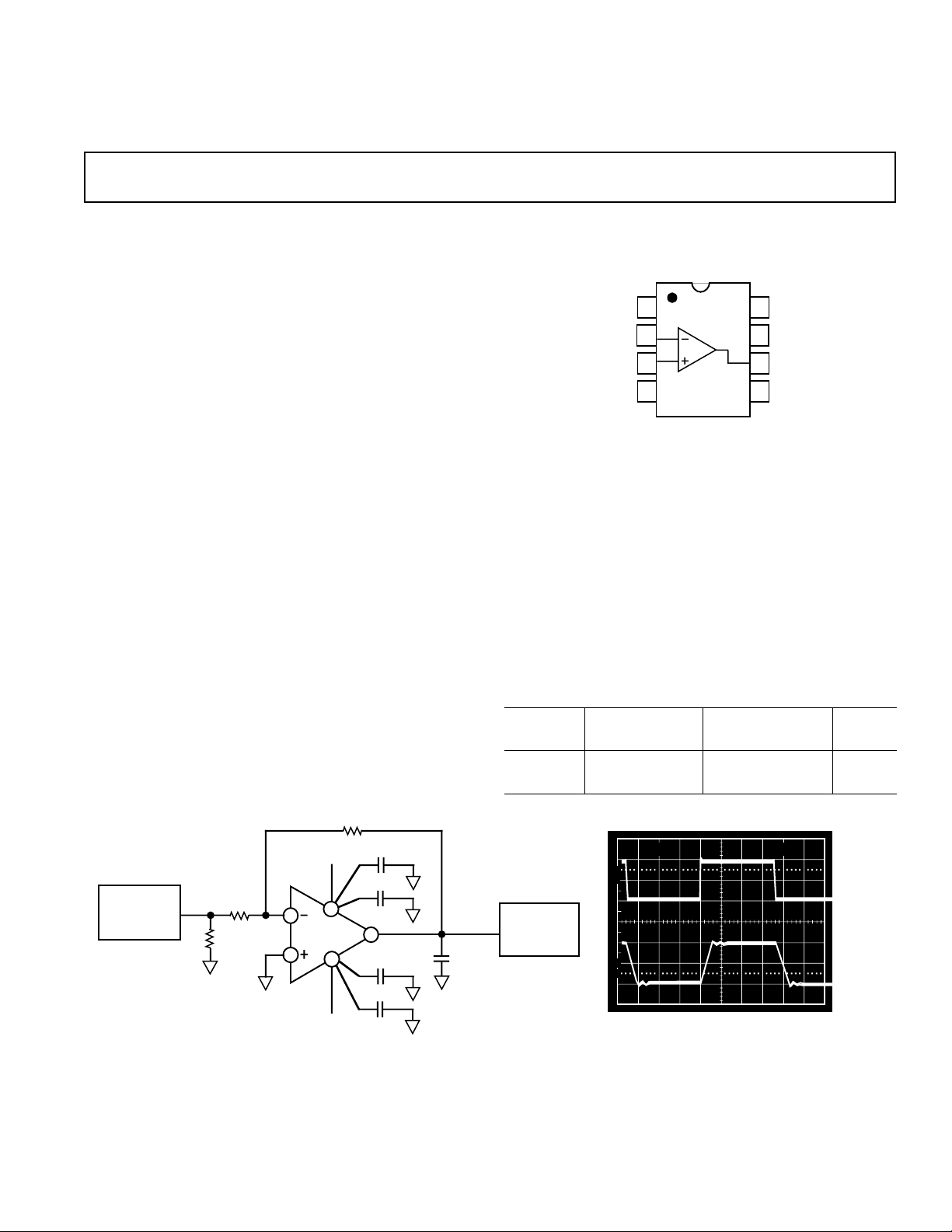
CONNECTION DIAGRAM
8-Pin Plastic Mini-DIP (N) and
SOIC (R) Packages
NULL
1
NULL
–IN
+IN
–V
S
AD817
2
3
4
TOP VIEW
NC = NO CONNECT
The AD817 is fully specified for operation with a single +5 V
power supply and with dual supplies from ± 5 V to ±15 V. This
power supply flexibility, coupled with a very low supply current
of 7.5 mA and excellent ac characteristics under all power supply conditions, make the AD817 the ideal choice for many demanding yet power sensitive applications.
In applications such as ADC buffers and line drivers the AD817
simplifies the design task with its unique combination of a
50 mA minimum output current and the ability to drive
unlimited capacitive loads.
The AD817 is available in 8-pin plastic mini-DIP and SOIC
packages.
ORDERING GUIDE
Temperature Package Package
Model Range Description Option
AD817AN –40°C to +85°C 8-Pin Plastic DIP N-8
AD817AR –40°C to +85°C 8-Pin Plastic SOIC R-8
8
7
6
5
+V
S
OUTPUT
NC
1kΩ
3.3µF
+V
S
0.01µF
HP
PUL SE
GENERATOR
1kΩ
V
IN
50Ω
2
3
7
AD817
4
–V
V
OUT
6
C
0.01µF
3.3µF
S
L
1000pF
AD817 Driving a Large Capacitive Load
REV. B
Information furnished by Analog Devices is believed to be accurate and
reliable. However, no responsibility is assumed by Analog Devices for its
use, nor for any infringements of patents or other rights of third parties
which may result from its use. No license is granted by implication or
otherwise under any patent or patent rights of Analog Devices.
5V
100
90
TEKTRONIX
P6201 FET
PROBE
10
0%
One Technology Way, P.O. Box 9106, Norwood. MA 02062-9106, U.S.A.
Tel: 617/329-4700 Fax: 617/326-8703
500ns
100pF
LOAD
1000pF
LOAD
© Analog Devices, Inc., 1995
Page 2

AD817–SPECIFICA TIONS
(@ TA = +258C, unless otherwise noted)
AD817A
Parameter Conditions V
S
Min Typ Max Units
DYNAMIC PERFORMANCE
Unity Gain Bandwidth ±5 V 30 35 MHz
±15 V 45 50 MHz
0, +5 V 25 29 MHz
Bandwidth for 0.1 dB Flatness Gain = +1 ±5 V 18 30 MHz
±15 V 40 70 MHz
Full Power Bandwidth
1
Slew Rate R
V
= 5 V p-p
OUT
R
= 500 Ω±5 V 15.9 MHz
LOAD
V
= 20 V p-p
OUT
R
= 1 kΩ±15 V 5.6 MHz
LOAD
= 1 kΩ±5 V 200 250 V/µs
LOAD
0, +5 V 10 20 MHz
Gain = 1 ±15 V 300 350 V/µs
0, +5 V 150 200 V/µs
Settling Time to 0.1% –2.5 V to +2.5 V ± 5 V 45 n s
0 V–10 V Step, A
= –1 ±15 V 45 ns
V
Settling Time to 0.01% –2.5 V to +2.5 V ± 5 V 70 ns
Total Harmonic Distortion F
0 V–10 V Step, A
= 1 MHz ±15 V 63 dB
C
= –1 ±15 V 70 ns
V
Differential Gain Error NTSC ±15 V 0.04 0.08 %
(R
= 150 Ω) Gain = +2 ±5 V 0.05 0.1 %
LOAD
0, +5 V 0.11 %
Differential Phase Error NTSC ±15 V 0.08 0.1 Degrees
(R
= 150 Ω) Gain = +2 ±5 V 0.06 0.1 Degrees
LOAD
0, +5 V 0.14 Degrees
INPUT OFFSET VOLTAGE ±5 V to ±15 V 0.5 2 mV
T
MIN
to T
MAX
3mV
Offset Drift 10 µV/°C
INPUT BIAS CURRENT ±5 V, ±15 V 3.3 6.6 µA
T
T
MIN
MAX
10 µA
4.4 µA
INPUT OFFSET CURRENT ±5 V, ±15 V 25 200 nA
T
MIN
to T
MAX
500 nA
Offset Current Drift 0.3 nA/°C
OPEN LOOP GAIN V
= ±2.5 V ±5 V
OUT
R
= 500 Ω 2 4 V/mV
LOAD
T
to T
R
V
R
T
V
R
MIN
LOAD
OUT
LOAD
MIN
OUT
LOAD
MAX
= 150 Ω 1.5 3 V/mV
= ±10 V ±15 V
= 1 kΩ 4 6 V/mV
to T
MAX
= ±7.5 V ±15 V
= 150 Ω
1.5 V/mV
2.5 5 V/mV
(50 mA Output) 2 4 V/mV
COMMON-MODE REJECTION V
= ±2.5 V ±5 78 100 dB
CM
V
= ±12 V ±15 V 86 120 dB
CM
±15 V 80 100 dB
POWER SUPPLY REJECTION VS = ±5 V to ±15 V 75 86 dB
T
MIN
to T
MAX
72 dB
INPUT VOLTAGE NOISE f = 10 kHz ±5 V, ±15 V 15 nV/√Hz
INPUT CURRENT NOISE f = 10 kHz ±5 V, ±15 V 1.5 pA/√Hz
–2–
REV. A
Page 3
AD817
MAXIMUM POWER DISSIPATION – Watts
AMBIENT TEMPERATURE – °C
2.0
1.5
0
–50 90–40 –30 –20 –10 0 10 20 30 50 60 70 8040
1.0
0.5
8-PIN MINI-DIP PACKAGE
8-PIN SOIC PACKAGE
TJ = +150°C
WARNING!
ESD SENSITIVE DEVICE
AD817A
Parameter Conditions V
S
INPUT COMMON-MODE ±5 V +3.8 +4.3 V
VOLTAGE RANGE –2.7 –3.4 V
±15 V +13 +14.3 V
0, +5 V +3.8 +4.3 V
Min Typ Max Units
–12 –13.4 V
+1.2 +0.9 V
OUTPUT VOLTAGE SWING R
= 500 Ω±5 V 3.3 3.8 ±V
LOAD
R
= 150 Ω±5 V 3.2 3.6 ±V
LOAD
R
= 1 kΩ±15 V 13.3 13.7 ±V
LOAD
R
= 500 Ω±15 V 12.8 13.4 ±V
LOAD
R
= 500 Ω 0, +5 V +1.5,
LOAD
+3.5 V
Output Current ±15 V 50 mA
±5 V 50 mA
0, +5 V 30 mA
Short-Circuit Current ±15 V 90 mA
INPUT RESISTANCE 300 kΩ
INPUT CAPACITANCE 1.5 pF
OUTPUT RESISTANCE Open Loop 8 Ω
POWER SUPPLY
Operating Range Dual Supply ±2.5 ±18 V
Single Supply +5 +36 V
Quiescent Current ±5 V 7.0 7.5 mA
T
MIN
to T
MAX
±5 V 7.5 mA
±15 V 7.5 mA
T
to T
MIN
NOTES
1
Full power bandwidth = slew rate/2 π V
Specifications subject to change without notice.
ABSOLUTE MAXIMUM RATINGS
Supply Voltage . . . . . . . . . . . . . . . . . . . . . . . . . . . . . . . . ±18 V
Internal Power Dissipation
2
PEAK
.
1
MAX
±15 V 7.0 7.5 mA
Plastic (N) . . . . . . . . . . . . . . . . . . . . . . See Derating Curves
Small Outline (R) . . . . . . . . . . . . . . . . . See Derating Curves
Input Voltage (Common Mode) . . . . . . . . . . . . . . . . . . . . ±V
S
Differential Input Voltage . . . . . . . . . . . . . . . . . . . . . . . . ±6V
Output Short Circuit Duration . . . . . . . . See Derating Curves
Storage Temperature Range N, R . . . . . . . . .–65°C to +125°C
Operating Temperature Range . . . . . . . . . . . . –40°C to +85°C
Lead Temperature Range (Soldering 10 sec) . . . . . . . . +300°C
NOTES
1
Stresses above those listed under “Absolute Maximum Ratings” may cause
permanent damage to the device. This is a stress rating only and functional
operation of the device at these or any other conditions above those indicated in the
operational section of this specification is not implied. Exposure to absolute
maximum rating conditions for extended periods may affect device reliability.
2
Specification is for device in free air: 8-pin plastic package: θJA = 100°C/watt;
8-pin SOIC package: θJA = 160°C/watt.
Maximum Power Dissipation vs. Temperature
CAUTION
ESD (electrostatic discharge) sensitive device. Electrostatic charges as high as 4000 V readily
accumulate on the human body and test equipment and can discharge without detection.
Although the AD817 features proprietary ESD protection circuitry, permanent damage may
occur on devices subjected to high energy electrostatic discharges. Therefore, proper ESD
precautions are recommended to avoid performance degradation or loss of functionality.
REV. B
–3–
Page 4
AD817–Typical Characteristics
-40°C
8.0
6.0
7.5
6.5
7.0
02051015
SUPPLY VOLTAGE – ±Volts
QUIESCENT SUPPLY CURRENT – mA
+25°C
+85°C
SLEW RATE – V/µs
20501510
SUPPLY VOLTAGE – ±Volts
200
300
350
400
250
20
15
+V
CM
10
–V
CM
5
INPUT COMMON-MODE RANGE – ± Volts
0
02051015
Figure 1. Common-Mode Voltage Range vs. Supply
20
15
SUPPLY VOLTAGE – ± Volts
Figure 4. Quiescent Supply Current vs. Supply Voltage
for Various Temperatures
10
5
OUTPUT VOLTAGE SWING – ±Volts
0
02051015
Figure 2. Output Voltage Swing vs. Supply
30
25
20
15
10
5
OUTPUT VOLTAGE SWING – Volts p-p
0
Figure 3. Output Voltage Swing vs. Load Resistance
RL = 500Ω
R
= 150Ω
L
SUPPLY VOLTAGE – ±Volts
VS = ±15V
VS = ±5V
LOAD RESISTANCE – Ω
Figure 5. Slew Rate vs. Supply Voltage
100
10
1
0.1
CLOSED-LOOP OUTPUT IMPEDANCE – Ohms
0.01
10k10010 1k
1k 10k 100M10M1M100k
FREQUENCY – Hz
Figure 6. Closed-Loop Output Impedance vs. Frequency
REV. B–4–
Page 5

AD817
100
10
30
20
40
50
60
70
80
90
100M1k100 10M1M100k10k
FREQUENCY – Hz
PSR – dB
POSITIVE
SUPPLY
NEGATIVE
SUPPLY
7
6
5
4
3
INPUT BIAS CURRENT – µA
2
1
TEMPERATURE – °C
Figure 7. Input Bias Current vs. Temperature
130
110
SOURCE CURRENT
90
SINK CURRENT
70
50
SHORT CIRCUIT CURRENT – mA
100
80
GAIN ±15V SUPPLIES
60
40
20
OPEN-LOOP GAIN – dB
140–40–60 120806040 100200–20
–20
0
GAIN ±5V SUPPLIES
= 1kΩ
R
L
FREQUENCY – Hz
PHASE ±5V OR
±15V SUPPLIES
+100
+80
+60
+40
+20
PHASE MARGIN – Degrees
0
1G10k1k 100M10M1M100k
Figure 10. Open-Loop Gain and Phase Margin
vs. Frequency
7
6
5
4
3
OPEN-LOOP GAIN – V/mV
2
±15V
±5V
30
TEMPERATURE – °C
Figure 8. Short Circuit Current vs. Temperature
100
80
60
40
PHASE MARGIN – Degrees
20
–60 140–40 100 120806040200–20
Figure 9. Unity Gain Bandwidth and Phase Margin
vs. Temperature
TEMPERATURE – °C
REV. B
PHASE MARGIN
GAIN BANDWIDTH
140–40–60 120100806040200–20
80
60
40
UNITY GAIN BANDWIDTH – MHz
20
–5–
1
100 1k 10k
LOAD RESISTANCE – Ohms
Figure 11. Open Loop Gain vs. Load Resistance
Figure 12. Power Supply Rejection vs. Frequency
Page 6

AD817–Typical Characteristics
–40
–100
–70
–90
–80
–50
–60
10M1k100 1M100k10k
FREQUENCY – Hz
HARMONIC DISTORTION – dB
VIN = 1V p-p
GAIN = +2
2nd HARMONIC
3rd HARMONIC
380
300
360
320
340
–60 140–40 100 120806040200–20
TEMPERATURE – °C
SLEW RATE – V/µs
120
100
80
CMR – dB
60
40
1k 10M10k 100k 1M
FREQUENCY – Hz
Figure 13. Common-Mode Rejection vs. Frequency
30
RL = 1kΩ
20
RL = 150Ω
10
OUTPUT VOLTAGE – Volts p-p
0
100k 1M 100M10M
FREQUENCY – Hz
Figure 14. Large Signal Frequency Response
OUTPUT SWING FROM 0 TO ±V
–10
10
8
6
4
1%
2
0
–2
1%
–4
–6
–8
0.1%
0.01%
0.01%
0.1%
SETTLING TIME – ns
Figure 15. Output Swing and Error vs. Settling Time
Figure 16. Harmonic Distortion vs. Frequency
50
40
30
20
10
INPUT VOLTAGE NOISE – nV/ Hz
0
FREQUENCY – Hz
10M1031M100k10k1k100
Figure 17. Input Voltage Noise Spectral Density
160200 140120100806040
Figure 18. Slew Rate vs. Temperature
REV. B–6–
Page 7

AD817
+V
S
TEKTRONIX
P6201 FET
PROBE
HP
PULSE (LS)
OR FUNCTION
(SS)
GENERATOR
100Ω
50Ω
1kΩ
R
L
V
OUT
0.01µF
3.3µF
–V
S
V
IN
TEKTRONIX
7A24
PREAMP
AD817
7
6
3
2
4
0.01µF
3.3µF
10
90
100
0%
50ns
5V
5V
DIFF GAIN
0.1
0.08
0.06
0.04
DIFFERENTIAL PHASE – Degrees
DIFF PHASE
SUPPLY VOLTAGE – Volts
Figure 19. Differential Gain and Phase vs.
Supply Voltage
5
4
3
V
IN
2
1
0
GAIN – dB
–1
–2
–3
–4
–5
100k 1M 100M10M
1kΩ
1kΩ
C
C
V
FREQUENCY – Hz
V
±15V
OUT
±5V
+5V
VS = ±5V
C
S
3pF
4pF
6pF
VS = +5V
0.1dB
FLATNESS
C
16MHz
14MHz
12MHz
VS = ±15V
0.05
0.04
0.03
DIFFERENTIAL GAIN – Percent
±15±5 ±10
Figure 22. Noninverting Amplifier Connection
REV. B
Figure 20. Closed-Loop Gain vs. Frequency,
Gain = –1
5
4
3
2
1
0
GAIN – dB
–1
–2
–3
–4
–5
100k 1M 100M10M
Figure 21. Closed-Loop Gain vs. Frequency,
V
IN
1kΩ
V
OUT
150Ω
FREQUENCY – Hz
V
S
±15V
±5V
+5V
VS = ±5V
VS = +5V
0.1dB
FLATNESS
70MHz
26MHz
17MHz
VS = ±15V
Gain = +1
–7–
Figure 23. Noninverting Large Signal Pulse
Response, R
200mV
100
90
10
0%
200mV
= 1 k
L
Ω
20ns
Figure 24. Noninverting Small Signal Pulse
Response, R
= 1 k
L
Ω
Page 8

AD817–Typical Characteristics
10
90
100
0%
5V
50ns
5V
10
90
100
0%
200mV
50ns
200mV
5V
100
90
10
0%
50ns
5V
Figure 25. Noninverting Large Signal Pulse
Response, R
100
90
= 150
L
Ω
20ns200mV
Figure 28. Inverting Large Signal Pulse
Response, R
= 1 k
L
Ω
10
0%
200mV
Figure 26. Noninverting Small Signal Pulse
Response, R
HP
PULSE (L
OR FUNCTION
(S
GENERATOR
)
SIG
V
IN
)
SIG
Figure 27. Inverting Amplifier Connection
1kΩ
50Ω
= 150
2
AD817
3
Ω
1kΩ
3.3µ F
+V
S
0.01µF
7
6
0.01µF
4
3.3µF
–V
S
TEKTRONIX
V
OUT
P6201 FET
PRO BE
R
L
TEKTRONIX
7A24
PREAMP
L
R
IN
Figure 29. Inverting Small Signal Pulse
Response, R
= 1 k
L
Ω
REV. B–8–
Page 9

AD817
+V
S
10kΩ
–V
S
AD817
7
3
2
4
8
6
1
VOS ADJUST
DRIVING CAPACITIVE LOADS
The internal compensation of the AD817, together with its high
output current drive, permit excellent large signal performance
while driving extremely high capacitive loads.
1kΩ
3.3µF
+V
S
0.01µF
R
HP
PULSE
GENERATOR
IN
V
1kΩ
IN
50Ω
2
AD817
3
7
6
0.01µF
4
3.3µF
–V
S
TEKTRONIX
V
OUT
P6201 FET
PROBE
C
L
1000pF
Figure 30a. Inverting Amplifier Driving a 1000 pF
Capacitive Load
5V
100
90
10
0%
5V
500ns
100pF
1000pF
Figure 30b. Inverting Amplifier Pulse Response While
Driving Capacitive Loads
THEORY OF OPERATION
The AD817 is a low cost, wide band, high performance operational amplifier which effectively drives heavy capacitive or resistive loads. It also provides a constant slew rate, bandwidth and
settling time over its entire specified temperature range.
The AD817 (Figure 31) consists of a degenerated NPN differential pair driving matched PNPs in a folded-cascode gain stage.
The output buffer stage employs emitter followers in a class AB
amplifier which delivers the necessary current to the load while
maintaining low levels of distortion.
The capacitor, C
, in the output stage mitigates the effect of
F
capacitive loads. At low frequencies, and with low capacitive
loads, the gain from the compensation node to the output is
very close to unity. In this case, C
is bootstrapped and does not
F
contribute to the overall compensation capacitance of the device.
As the capacitive load is increased, a pole is formed with the
output impedance of the output stage. This reduces the gain,
and therefore, C
some fraction of C
is incompletely bootstrapped. Effectively,
F
contributes to the overall compensation
F
capacitance, reducing the unity gain bandwidth. As the load
capacitance is further increased, the bandwidth continues to fall,
maintaining the stability of the amplifier.
REV. B
TEKTRONIX
7A24
PREAMP
+V
S
OUTPUT
–V
S
–IN
+IN
NULL 1 NULL 8
C
F
Figure 31. Simplified Schematic
INPUT CONSIDERATIONS
An input protection resistor (RIN in Figure 22) is required in circuits where the input to the AD817 will be subjected to transient or continuous overload voltages exceeding the +6 V
maximum differential limit. This resistor provides protection for
the input transistors by limiting their maximum base current.
For high performance circuits, it is recommended that a “balancing” resistor be used to reduce the offset errors caused by
bias current flowing through the input and feedback resistors.
The balancing resistor equals the parallel combination of R
and RF and thus provides a matched impedance at each input
terminal. The offset voltage error will then be reduced by more
than an order of magnitude.
GROUNDING & BYPASSING
When designing high frequency circuits, some special precautions are in order. Circuits must be built with short interconnect
leads. When wiring components, care should be taken to provide a low resistance, low inductance path to ground. Sockets
should be avoided, since their increased interlead capacitance
can degrade circuit bandwidth.
Feedback resistors should be of low enough value (<1 kΩ) to
assure that the time constant formed with the inherent stray
capacitance at the amplifier’s summing junction will not limit
performance. This parasitic capacitance, along with the parallel
resistance of R
, form a pole in the loop transmission which
F/RIN
may result in peaking. A small capacitance (1 pF–5 pF) may be
used in parallel with the feedback resistor to neutralize this effect.
Power supply leads should be bypassed to ground as close as
possible to the amplifier pins. Ceramic disc capacitors of 0.1 µF
are recommended.
Figure 32. Offset Null Configuration
–9–
IN
Page 10

AD817
0.05
0.05
0
0.20
0.10
0.15
–10
–6
–4
0
–2
–8
0 350 40030025020015010050
SETTLING TIME TO %
OF FINAL VALUE
OUTPUT SWING – Volts
OFFSET NULLING
The input offset voltage of the AD817 is inherently very low.
However, if additional nulling is required, the circuit shown in
Figure 32 can be used. The null range of the AD817 in this configuration is ±15 mV.
AD817 SETTLING TIME
Settling time is comprised primarily of two regions. The first is
the slew time in which the amplifier is overdriven, where the
output voltage rate of change is at its maximum. The second is
the linear time period required for the amplifier to settle to
within a specified percent of the final value.
10
8
6
4
2
0
OUTPUT SWING – Volts
0.05
0
0.05
0.10
0.15
OF FINAL VALUE
0.20
SETTLING TIME TO %
0 350 40030025020015010050
Measuring the rapid settling time of AD817 (45 ns to 0.1% and
70 ns to 0.01%–10 V step) requires applying an input pulse with
a very fast edge and an extremely flat top. With the AD817 configured in a gain of –1, a clamped false summing junction responds when the output error is within the sum of two diode
voltages (ª1 volt). The signal is then amplified 20 times by a
clamped amplifier whose output is connected directly to a sampling oscilloscope. Figures 33 and 34 show the settling time of
the AD817, with a 10 volt step applied.
Figure 34. Settling Time in ns 0 V to –10 V
Figure 33. Settling Time in ns 0 V to +10 V
ERROR AMPLIFIER
V
OUTPUT × 10
ERROR
2×
HP2835
ERROR
SIGNAL
OUTPUT
0 TO ±10V
TTL LEVEL
SIGNAL
GENERATOR
50Hz
OUTPUT
DIGITAL
GROUND
ANALOG
GROUND
POWER
SUPPLY
7, 8
2
13
1, 14
EI&S
DL1A05GM
MERCURY RELAY
50Ω
COAX
CABLE
1kΩ 100Ω 1kΩ
500Ω
50Ω
2.2µF
Figure 35. Settling Time Test Circuit
0.01µF
NULL
ADJUST
3
2
0.47µF
2
3
0.01µF
–10–
AD829
7
–V
1.9kΩ100Ω
FALSE
SUMMING
NODE
500Ω
AD817
4
–V
S
5
+V
S
5–18pF
7
+V
S
4
2.2µF
S
2×
HP2835
6
0.47µF
0.01µF
6
1MΩ
100Ω
SHORT, DIRECT
CONNECTION TO
TEKTRONIX TYPE 11402
OSCILLOSCOPE PREAMP
INPUT SECTION
NOTE:
USE CIRCUIT BOARD
WITH GROUND PLANE
DEVICE
UNDER
TEST
10pF
SCOPE PROBE
0.01µF
CAPACITANCE
15pF
SETTLING
OUTPUT
TEKTRONIX P6201
FET PROBE TO
TEKTRONIX TYPE
11402
OSCILLOSCOPE
PREAMP INPUT
SECTION
REV. B
Page 11

AD817
A HIGH PERFORMANCE ADC INPUT BUFFER
High performance analog to digital converters (ADCs) require
input buffers with correspondingly high bandwidths and very
low levels of distortion. Typical requirements include distortion
levels of –60 dB to –70 dB for a 1 volt p-p signal and bandwidths of 10 MHz or more. In addition, an ADC buffer may
need to drive very large capacitive loads.
The circuit of Figure 36 is useful for driving high speed converters such as the differential input of the AD733, 10-bit ADC.
This circuit may be used with other converters with only minor
modifications. Using the AD817 provides the user with the option of either operating the buffer in differential mode or from a
single +5 volt supply. Operating from a +5 volt power supply
helps to avoid overdriving the ADC—a common problem with
buffers operating at higher supply voltages.
SINGLE SUPPLY OPERATION
Another exciting feature of the AD817 is its ability to perform
well in a single supply configuration. The AD817 is ideally
suited for applications that require low power dissipation and
high output current and those which need to drive large capacitive loads, such as high speed buffering and instrumentation.
Referring to Figure 37, careful consideration should be given to
the proper selection of component values. The choices for this
particular circuit are: R1+ R3//R2 combine with C1 to form a
low frequency corner of approximately 300 Hz.
+V
S
R3
1kΩ
C2
0.1µF
0.1µ F
V
IN
R1
9kΩ
C1
R2
10kΩ
2
3
7
AD817
4
3.3µF
0.01µF
6
SELECT C1, R1, R2 & R3
FOR DESIRED LOW
FREQUENCY CORNER.
(R2 = R1 + R3)
R
L
150Ω
C3
0.1µF
C
OUT
C
200pF
V
OUT
L
Figure 37. Single Supply Amplifier Configuration
Combining R3 with C2 forms a low-pass filter with a corner
frequency of 1.5 kHz. This is needed to maintain amplifier
PSRR, since the supply is connected to V
divider. The values for R
and CL were chosen to demonstrate
L
through the input
IN
the AD817’s exceptional output drive capability. In this configuration, the output is centered around 2.5 V. In order to
eliminate the static dc current associated with this level, C3 was
inserted in series with R
.
L
1kΩ
+V
S
0.1µF
V
500mVp-p
MAX
COMMON
IN
+5V
–5V
50Ω
COAX
CABLE
100µF
25V
100µF
25V
52.5Ω
1kΩ
1kΩ
+V
S
–V
S
2
3
3
2
7
AD817
4
–V
+V
7
AD817
4
–V
1kΩ
6
0.1µF
S
S
0.1µF
6
0.1µF
S
Figure 36. A Differential Input Buffer for High Bandwidth ADCs
V
26
INA
AD773
10-BIT
18MHz
V
27
INB
ADREF43
VOLTAGE
REFERENCE
ADC
+2.5V
REV. B
–11–
Page 12

AD817
0.0098 (0.25)
0.0075 (0.19)
0.0500 (1.27)
0.0160 (0.41)
8
°
0
°
0.0196 (0.50)
0.0099 (0.25)
x 45
°
PIN 1
0.1574 (4.00)
0.1497 (3.80)
0.2440 (6.20)
0.2284 (5.80)
4
5
1
8
0.0192 (0.49)
0.0138 (0.35)
0.0500
(1.27)
BSC
0.0688 (1.75)
0.0532 (1.35)
0.0098 (0.25)
0.0040 (0.10)
0.1968 (5.00)
0.1890 (4.80)
HIGH SPEED DAC BUFFER
The wide bandwidth and fast settling time of the AD817 make
it a very good output buffer for high speed current output D/A
converters like the AD668. As shown in Figure 38, the op amp
establishes a summing node at ground for the DAC output. The
output voltage is determined by the amplifier’s feedback resistor
+15V
10µF
0.1µF
DIGITAL
INPUTS
1
2
3
4
5
6
7
8
9
10
11
12
MSB
REFCOM
AD668
LSB
V
REFIN1
REFIN2
I
OUT
R
LOAD
ACOM
LCOM
IBPO
V
THCOM
VTH
24
CC
23
22
21
20
19
18
17
16
15
EE
14
13
ANALOG GROUND PLANE
100pF
(10.24 V for a 1 kΩ resistor). Note that since the DAC generates a positive current to ground, the voltage at the amplifier
output will be negative. A 100 Ω series resistor between the
noninverting amplifier input and ground minimizes the offset
effects of op amp input bias currents.
TO ANALOG
GROUND PLANE
1V NOMINAL
REFERENCE INPUT
10kΩ
1kΩ
100Ω
AD817
10µF
0.1µF
–15V
1kΩ
+5V
ANALOG
OUTPUT
ANALOG
SUPPLY
GROUND
C1707b–5–6/95
PIN 1
0.165±0.01
(4.19±0.25)
0.125
(3.18)
MIN
0.018±0.003
(0.46±0.08)
8-Pin Plastic Mini-DIP
(N-8)
58
0.25
(6.35)
0.31
0.035±0.01
(0.89±0.25)
0.18±0.03
(4.57±0.76)
SEATING
PLANE
(7.87)
1
0.39 (9.91) MAX
0.10
(2.54)
BSC
0.033
(0.84)
NOM
4
Figure 38. High Speed DAC Buffer
OUTLINE DIMENSIONS
Dimensions shown in inches and (mm).
0.30 (7.62)
REF
0.011±0.003
(0.28±0.08)
15
°
0
°
8-Pin SOIC
(SO-8)
PRINTED IN U.S.A.
–12–
REV. B
 Loading...