

Datasheet AD8174AR-REEL, AD8174AR, AD8174AN, AD8170AR-REEL, AD8170AR Datasheet (Analog Devices)
...Page 1
a
1
2
3
4
8
7
6
5
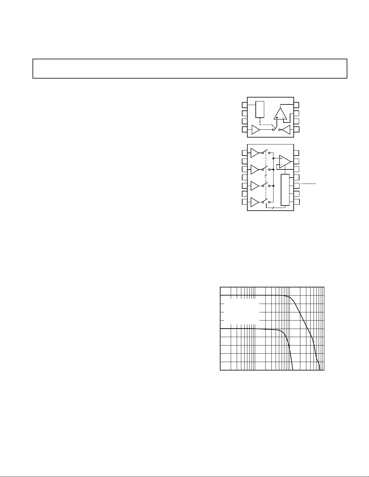
AD8170
+1 +1
LOGIC
V
OUT
–V
IN
+V
S
IN1
SELECT
GND
–V
S
IN0
10
9
8
+1
AD8174
+1
+1
+1
2
2
14
13
12
11
1
2
3
4
5
6
7
LOGIC
+V
S
V
OUT
–V
IN
SD
ENABLE
A1
A0
IN0
GND
IN1
GND
IN2
–V
S
IN3
250 MHz, 10 ns Switching
Multiplexers w/Amplifier
AD8170/AD8174
FEATURES
Fully Buffered Inputs and Outputs
Fast Channel Switching: 10 ns
Internal Current Feedback Output Amplifier
High Output Drive: 50 mA
Flexible Gain Setting via External Resistor(s)
High Speed
250 MHz Bandwidth, G = +2
1000 V/ms Slew Rate
Fast Settling Time of 15 ns to 0.1%
Low Power: < 10 mA
Excellent Video Specifications (R
= 150 V, G = +2)
L
Gain Flatness of 0.1 dB Beyond 80 MHz
0.02% Differential Gain Error
0.058 Differential Phase Error
Low Crosstalk of –78 dB @ 5 MHz
High Disable Isolation of –88 dB @ 5 MHz
High Shutdown Isolation of –92 dB @ 5 MHz
Low Cost
Fast Output Disable Feature for Connecting Multiple
Devices (AD8174 Only)
Shutdown Feature Reduces Power to 1.5 mA (AD8174 Only)
APPLICATIONS
Pixel Switching for “Picture-In-Picture”
LCD and Plasma Displays
Video Routers
PRODUCT DESCRIPTION
The AD8170(2:1) and AD8174(4:1) are very high speed
buffered multiplexers. These multiplexers offer an internal
current feedback output amplifier whose gain can be programmed via external resistors and is capable of delivering 50
mA of output current. They offer –3 dB signal bandwidth of
250 MHz and slew rate of greater than 1000 V/µs. Additionally,
the AD8170 and AD8174 have excellent video specifications
with low differential gain and differential phase error of 0.02%
and 0.05° and 0.1 dB flatness out to 80 MHz. With a low 78
dB of crosstalk and better than 88 dB isolation, these devices are
useful in many high speed applications. These are low power
devices consuming only 9.7 mA from a ± 5 V supply.
FUNCTIONAL BLOCK DIAGRAM
The AD8174 offers a high speed disable feature allowing the
output to be put into a high impedance state for cascading
stages so that the off channels do not load the output bus.
Additionally, the AD8174 can be shut down (SD) when not in
use to minimize power consumption (I
= 1.5 mA). These
S
products will be offered in 8-lead and 14-lead PDIP and SOIC
packages.
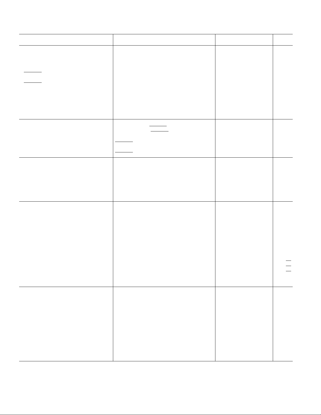
VIN = 50mV rms
G = +2
= 499Ω (AD8170R)
R
F
= 549Ω (AD8174R)
R
F
0.1
= 100Ω
R
L
0
–0.1
–0.2
–0.3
–0.4
NORMALIZED FLATNESS – dB
–0.5
1M 10M 100M 1G
FREQUENCY – Hz
0
–1
–2
–3
–4
–5
–6
–7
NORMALIZED OUTPUT – dB
–8
–9
Figure 1. Small Signal Frequency Response
REV. 0
Information furnished by Analog Devices is believed to be accurate and
reliable. However, no responsibility is assumed by Analog Devices for its
use, nor for any infringements of patents or other rights of third parties
which may result from its use. No license is granted by implication or
otherwise under any patent or patent rights of Analog Devices.
One Technology Way, P.O. Box 9106, Norwood, MA 02062-9106, U.S.A.
Tel: 617/329-4700 World Wide Web Site: http://www.analog.com
Fax: 617/326-8703 © Analog Devices, Inc., 1996
Page 2
(@ TA = +258C, VS = 65 V, RL = 150 V, G = +2, RF = 499 V
AD8170/AD8174–SPECIFICATIONS
Parameter Conditions Min Typ Max Units
SWITCHING CHARACTERISTICS
Switching Time
1
50% Logic to 10% Output Settling IN0, IN2 = +0.5 V; IN1, IN3 = –0.5 V 7.5 ns
50% Logic to 90% Output Settling IN0, IN2 = +0.5 V; IN1, IN3 = –0.5 V 9.1 ns
50% Logic to 99.9% Output Settling IN0, IN2 = +0.5 V; IN1, IN3 = –0.5 V 25 ns
ENABLE to Channel ON Time2 (AD8174R)
50% Logic to 90% Output Settling IN0, IN2 = +0.5 V; IN1, IN3 = –0.5 V 17 ns
ENABLE to Channel OFF Time2 (AD8174R)
50% Logic to 90% Output Settling IN0, IN2 = +0.5 V; IN1, IN3 = –0.5 V 120 ns
Shutdown to Channel ON Time
50% Logic to 90% Output Settling IN0, IN2 = +0.5 V; IN1, IN3 = –0.5 V 20 ns
Shutdown to Channel OFF Time
50% Logic to 90% Output Settling IN0, IN2 = +0.5 V; IN1, IN3 = –0.5 V 115 ns
Channel Switching Transient (Glitch)
3
(AD8174R)
3
(AD8174R)
4
DIGITAL INPUTS
Logic “1” Voltage SELECT, A0, A1,
Logic “0” Voltage SELECT, A0, A1,
Logic “1” Input Current SELECT, A0, A1 Inputs, T
Logic “0” Input Current SELECT, A0, A1 Inputs, T
DYNAMIC PERFORMANCE
–3 dB Bandwidth (Small Signal)
–3 dB Bandwidth (Large Signal)
0.1 dB Bandwidth
5
5
5
Rise and Fall Time (10% to 90%) 2 V Step 1.6 ns
Slew Rate 2 V Step 1000 V/µs
Settling Time to 0.1% 2 V Step 15 ns
DISTORTION/NOISE PERFORMANCE
Differential Gain ƒ = 3.58 MHz 0.02 %
Differential Phase ƒ = 3.58 MHz 0.05
All Hostile Crosstalk
All Hostile Crosstalk
Disable Isolation
Shutdown Isolation
6
6
7
8
AD8170R ƒ = 5 MHz, RL = 100 Ω –80 dB
AD8174R ƒ = 5 MHz, RL = 100 Ω –78 dB
AD8174R ƒ = 5 MHz, RL = 100 Ω –88 dB
AD8174R ƒ = 5 MHz, RL = 100 Ω –92 dB
Input Voltage Noise ƒ = 10 kHz to 30 MHz 10 nV/√
+Input Current Noise ƒ = 10 kHz to 30 MHz 1.6 pA/√
–Input Current Noise ƒ = 10 kHz to 30 MHz 8.5 pA/√
Total Harmonic Distortion ƒ
DC/TRANSFER CHARACTERISTICS
Transresistance 400 600 kΩ
Open-Loop Voltage Gain 2000 6000 V/V
Gain Accuracy
9
Gain Matching Channel-to-Channel 0.05 %
Input Offset Voltage 59mV
Input Offset Voltage Matching Channel-to-Channel 1.5 5 mV
Input Offset Voltage Drift 11 µV/°C
Input Bias Current (+) Switch Input 7 15 µA
Input Bias Current Drift (+) Switch and (–) Buffer Input 20 nA/°C
AD8170A/AD8174A
Channel-to-Channel
All Inputs Grounded 138 /104 mV p-p
ENABLE, SD Inputs, T
ENABLE, SD Inputs, T
VO = 50 mV rms, RL = 100 Ω 250 MHz
VO = 1 V rms, RL = 100 Ω 100 MHz
VO = 50 mV rms, RF = 499 Ω (AD8170R), RL = 100 Ω
= 50 mV rms, RF = 549 Ω (AD8174R), RL = 100 Ω 85 MHz
V
O
ƒ = 30 MHz, R
ƒ = 30 MHz, R
ƒ = 30 MHz, R
ƒ = 30 MHz, R
= 10 MHz, VO = 2 V p-p, RL = 150 Ω –60 dBc
C
= 100 Ω –65 dB
L
= 100 Ω –63 dB
L
= 100 Ω –72 dB
L
= 100 Ω –77 dB
L
ƒC = 10 MHz, VO = 2 V p-p, RL = 1 kΩ –72 dBc
G = +1, RF = 1 kΩ 0.4 %
to T
T
MIN
T
MIN
to T
MAX
MAX
(–) Buffer Input 3 10 µA
to T
T
MIN
MAX
(AD8170R), RF = 549 V (AD8174R) unless otherwise noted)
ENABLE, SD Inputs, T
ENABLE, SD Inputs, T
MIN–TMAX
MIN–TMAX
MIN–TMAX
MIN–TMAX
MIN–TMAX
MIN–TMAX
2.0 V
50 300 nA
15µA
35µA
30 300 nA
0.8 V
Degrees
Hz
Hz
Hz
12 mV
15 µA
14 µA
–2–
REV. 0
Page 3
AD8170/AD8174
AD8170A/AD8174A
Parameter Conditions Min Typ Max Units
INPUT CHARACTERISTICS
Input Resistance (+) Switch Input 1.7 MΩ
Input Capacitance Channel Enabled (R Package) 1.1 pF
Input Voltage Range ±3.3 V
Input Common-Mode Rejection Ratio +CMRR, ∆V
OUTPUT CHARACTERISTICS
Output Voltage Swing R
Output Current R
Short Circuit Current 180 mA
Output Resistance Enabled 10 mΩ
Output Capacitance Disabled (AD8174) 7.5 pF
POWER SUPPLY
Operating Range ±4 ±6V
Power Supply Rejection Ratio +PSRR +V
Power Supply Rejection Ratio –PSRR –V
Quiescent Current All Channels “ON”, T
OPERATING TEMPERATURE RANGE –40 +85 °C
NOTES
1
Shutdown (SD) and ENABLE pins are grounded (AD8174). IN0 (or IN2) = +0.5 V dc, IN1 (or IN3) = –0.5 V dc. SELECT (A0 or A1 for AD8174) input is
driven with 0 V to +5 V pulse. Measure transition time from 50% of SELECT (A0 or A1) input value (+2.5 V) and 10% (or 90%) of the total output voltage transition from IN0 (or IN2) channel voltage (+0.5 V) to IN1 (or IN3 = –0.5 V) or vice versa.
2
AD8174 only. Shutdown (SD) pin is grounded. ENABLE pin is driven with 0 V to +5 V pulse (5 ns rise and fall times). State of A0 and A1 logic inputs determines
which channel is activated (i.e., if A0 = Logic 0 and A1 = Logic 1, then IN2 input is selected). Set IN0 (or IN2) = +0.5 V dc, IN1 (or IN3) = –0.5 V dc, and measure transition time from 50% of ENABLE pulse (+2.5 V) to 90% of the total output voltage change. In Figure 5, ∆t
3
AD8174 only. ENABLE pin is grounded. Shutdown (SD) pin is driven with 0 V to +5 V pulse (5 ns rise and fall times). State of A0 and A1 logic inputs determines
which channel is activated (i.e., if A0 = Logic 1 and A1 = Logic O, then IN1 input is selected). Set IN0 (or IN2) = +0.5 V dc, IN1 (or IN3) = –0.5 V dc, and measure transition time from 50% of SD pulse (+2.5 V) to 90% of the total output voltage change. In Figure 6, ∆ t
release time.
4
All inputs are grounded. SELECT (A0 or A1 for AD8174) input is driven with 0 V to +5 V pulse. The outputs are monitored. Speeding the edges of the SELECT
(A0 or A1) pulse increases the glitch magnitude due to coupling via the ground plane.
5
Bandwidth of the multiplexer is dependent upon the resistor feedback network. Refer to Table III for recommended feedback component values, which give the best
compromise between a wide and a flat frequency response.
6
Select input(s) that is (are) not being driven (i.e., if SELECT is Logic 1, activated input is IN1; in AD8174, if A0 = Logic 0, A1 = Logic 1, activated input is IN2).
Drive all other inputs with VIN = 0.707 V rms, and monitor output at f = 5 MHz and 30 MHz; RL = 100 Ω (see Figure 13).
7
AD8174 only. Shutdown (SD) pin is grounded. Mux is disabled, (i.e., ENABLE = Logic 1) and all inputs are driven simultaneously with VIN = 0.354 V rms. Output is monitored at f = 5 MHz and 30 MHz; RL = 100 Ω. In this mode, the output impedance of the disabled mux is very high (typ 10 MΩ), and the signal couples
across the package; the load impedance and the feedback network determine the crosstalk. For instance, in a closed-loop gain of +1, r
(RF = RG = 549 Ω), r
8
AD8174 only. ENABLE pin is grounded. Mux is shutdown (i.e., SD = Logic 1), and all inputs are driven simultaneously with VIN = 0.354 V rms. Output is monitored at f = 5 MHz and 30 MHz; RL = 100 Ω. (see Figure 14). The mux output impedance in shutdown mode is the same as the disabled mux output impedance.
9
For Gain Accuracy expression, refer to Equation 4.
Specifications subject to change without notice.
= 1.1 kΩ (see Figure 14).
OUT
(–) Buffer Input 100 Ω
Channel Disabled (R Package) 1.1 pF
= 1 V 51 56 dB
CM
–CMRR, ∆VCM = 1 V 50 52 dB
= 1 kΩ, T
L
= 150 Ω, T
R
L
= 10 Ω 50 mA
L
MIN–TMAX
MIN–TMAX
±4.0 ±4.26 V
±3.5 ±4.0 V
Disabled (AD8174) 10 MΩ
= +4.5 V to +5.5 V, –VS = –5 V 58 66 dB
S
T
MIN–TMAX
= –4.5 V to –5.5 V, +VS= +5 V 52 58 dB
S
T
MIN–TMAX
AD8174 Disabled, T
AD8174 Shutdown, T
MIN–TMAX
MIN–TMAX
MIN–TMAX
55 dB
50 dB
8.7/9.7 11/13 mA
4.1 5 mA
1.5 2.5 mA
is the disable time, ∆tON is the enable time.
OFF
is the shutdown assert time, ∆t
OFF
ù 10 MΩ, in a gain of +2
OUT
is the shutdown
ON
REV. 0
Table I. AD8170 Truth Table
SELECT V
0 IN0
1 IN1
OUT
Table II. AD8174 Truth Table
A0 A1 ENABLE SD V
OUT
0 0 0 0 IN0
1 0 0 0 IN1
0 1 0 0 IN2
1 1 0 0 IN3
X X 1 0 HIGH Z, I
= 4.1 mA
S
X X X 1 HIGH Z, IS = 1.5 mA
–3–
Page 4
AD8170/AD8174
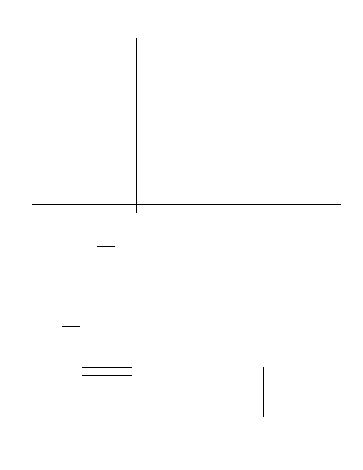
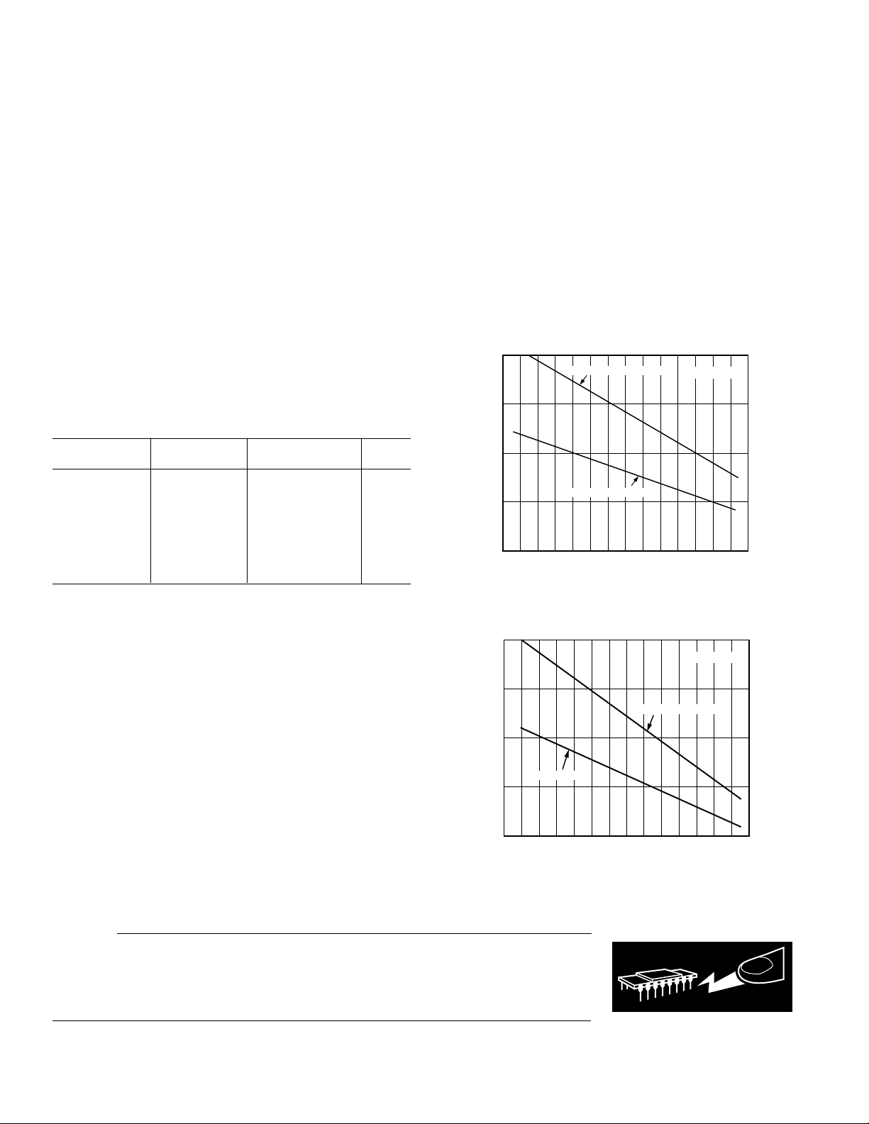
WARNING!
ESD SENSITIVE DEVICE
MAXIMUM POWER DISSIPATION – Watts
AMBIENT TEMPERATURE – °C
2.0
1.5
0
–50 90–40 –30 –20 –10 0 10 20 30 50 60 70 8040
1.0
0.5
8-PIN MINI-DIP PACKAGE
8-PIN SOIC PACKAGE
TJ = +150°C
AMBIENT TEMPERATURE – °C
2.5
2.0
0.5
–50 90–40
MAXIMUM POWER DISSIPATION – Watts
–30 –20 –10 0 10 20 30 40 50 60 80
1.5
1.0
70
14-PIN SOIC
14-PIN DIP PACKAGE
TJ = +150°C
ABSOLUTE MAXIMUM RATINGS
Supply Voltage . . . . . . . . . . . . . . . . . . . . . . . . . . . . . . . .12.6 V
Internal Power Dissipation
2
1
AD8170 8-Lead Plastic (N) . . . . . . . . . . . . . . . . . 1.3 Watts
AD8170 8-Lead Small Outline (R) . . . . . . . . . . . 0.9 Watts
AD8174 14-Lead Plastic (N) . . . . . . . . . . . . . . . . 1.6 Watts
AD8174 14-Lead Small Outline (R) . . . . . . . . . . 1.0 Watts
Input Voltage (Common Mode) . . . . . . . . . . . . . . . . . . . . ±V
S
Output Short Circuit Duration . . Observe Power Derating Curves
Storage Temperature Range
N & R Packages . . . . . . . . . . . . . . . . . . . . –65°C to +125°C
Lead Temperature Range (Soldering 10 sec) . . . . . . . .+300°C
NOTES
1
Stresses above those listed under “Absolute Maximum Ratings” may cause
permanent damage to the device. This is a stress rating only and functional
operation of the device at these or any other conditions above those indicated in
the operational section of this specification is not implied. Exposure to absolute
maximum rating conditions for extended periods may affect device reliability.
2
Specification is for device in free air: 8-Pin Plastic Package: θJA = 90°C/Watt;
8-Pin SOIC Package: θJA = 160°C/Watt; 14-Pin Plastic Package: θJA = 90°C/Watt
14-Pin SOIC Package: θJA = 120°C/Watt, where PD = (TJ–TA)/θJA.
ORDERING GUIDE
Temperature Package Package
Model Range Description Option
AD8170AN –40°C to +85°C 8-Pin Plastic DIP N-8
AD8170AR –40°C to +85°C 8-Pin SOIC SO-8
AD8170AR-REEL –40°C to +85°C Reel 8-Pin SOIC SO-8
AD8174AN –40°C to +85°C 14-Pin Plastic DIP N-14
AD8174AR –40°C to +85°C 14-Pin Narrow SOIC R-14
AD8174AR-REEL –40°C to +85°C Reel 14-Pin SOIC R-14
AD8170-EB Evaluation Board For AD8170R
AD8174-EB Evaluation Board For AD8174R
MAXIMUM POWER DISSIPATION
The maximum power that can be safely dissipated by the
AD8170 and AD8174 is limited by the associated rise in
junction temperature. The maximum safe junction temperature
for plastic encapsulated devices is determined by the glass
transition temperature of the plastic, approximately +150°C.
Exceeding this limit temporarily may cause a shift in parametric
performance due to a change in the stresses exerted on the die
by the package. Exceeding a junction temperature of +175°C
for an extended period can result in device failure.
While the AD8170 and AD8174 are internally short circuit
protected, this may not be sufficient to guarantee that the maximum junction temperature (+150°C) is not exceeded under all
conditions. To ensure proper operation, it is necessary to observe
the maximum power derating curves shown in Figures 2 and 3.
Figure 2. AD8170 Maximum Power Dissipation vs.
Temperature
CAUTION
ESD (electrostatic discharge) sensitive device. Electrostatic charges as high as 4000 V readily
accumulate on the human body and test equipment and can discharge without detection.
Although the AD8170/AD8174 feature proprietary ESD protection circuitry, permanent damage
may occur on devices subjected to high energy electrostatic discharges. Therefore, proper ESD
Figure 3. AD8174 Maximum Power Dissipation vs.
Temperature
precautions are recommended to avoid performance degradation or loss of functionality.
–4–
REV. 0
Page 5
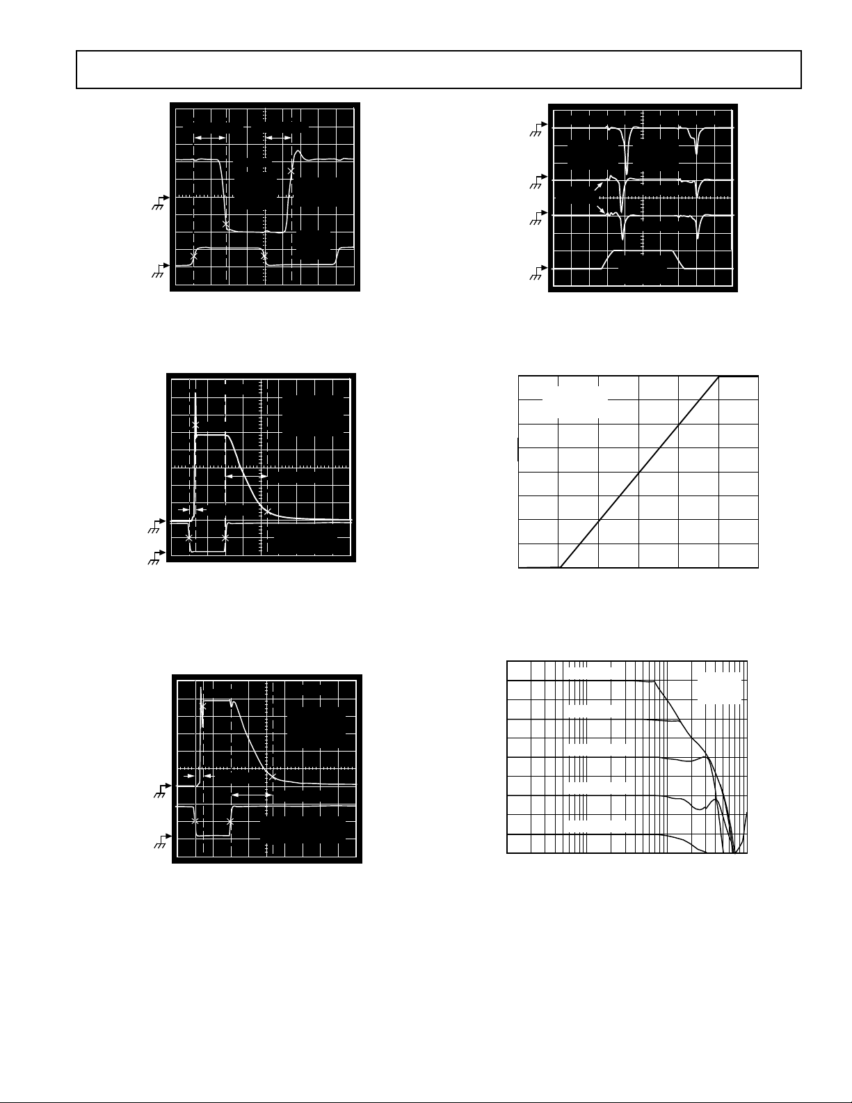
Typical Performance Characteristics – AD8170/AD8174
∆t
RISE
IN0, IN2 =
+0.5V
IN1, IN3 =
+0.5V
5ns/DIV
= 7.5ns
G = +2
R
R
= RG = 499V
F
= 100V
L
SELECT
PULSE
0 TO +5V
DUT
OUT
500mV/DIV
∆t
= 9.1ns
FALL
OUTPUT
Figure 4. Channel Switching Characteristics
AD8174R
OUTPUT
200mV/DIV
∆tON = 17ns
∆t
ENABLE PULSE
50ns/DIV
INØ = +0.5VDC
G = +2
= 549V
R
F
R
= 100V
L
= 120ns
OFF
0 TO +5V
(5nsec EDGES)
OUTPUT (AD8170R)
OUTPUT
(AD8174R)
50mV/DIV
G = +2
= 499V
R
F
(AD8170R)
SEL SWITCHING
RF = 549V
(AD8174R)
R
= 100V
L
A0 SWITCHING
A1 SWITCHING
SEL, A0, A1
PULSE
0 TO +5V
10ns/DIV
Figure 7. Switching Transient (Glitch) Response
4
G = +2
3
2
1
0
– Volts
OUT
V
–1
–2
–3
–4
= RG = 1kΩ
R
F
R
= 150Ω
L
–3
–2–10123
V
IN
– Volts
Figure 5. Enable and Disable Switching Characteristics
OUTPUT
∆tON = 20ns
200mV/DIV
AD8174R
INØ = +0.5VDC
G = +2
= 549V
R
F
R
= 100V
L
∆t
= 115ns
OFF
SHUTDOWN PULSE
0 TO +5V
(5nsec EDGES)
50ns/DIV
Figure 6. Shutdown Switching Characteristics
Figure 8. Output Voltage vs. Input Voltage, G = +2
= 549Ω
= 100Ω
9
0
–3
–6
–9
–12
–15
–18
–21
–24
–27
9
6
3
0
–3
–6
–9
–12
OUTPUT LEVEL – dBV
–15
–18
–21
1M 1G10M
VIN = 1.0V rms
VIN = 0.5V rms
VIN = 0.25V rms
VIN = 125mV rms
VIN = 625mV rms
FREQUENCY – Hz
100M
G = +2
R
F
R
L
Figure 9. Large Signal Frequency Response
INPUT LEVEL – dBV
REV. 0
–5–
Page 6

AD8170/AD8174
FREQUENCY – Hz
–20
–30
–10
0.1 1G1M 10M 100M
–60
–90
–100
–110
–40
–50
–80
–70
CROSSTALK – dB
VIN = +0.707V rms
G = +2
R
F
= 499Ω (AD8170R)
R
F
= 549Ω (AD8174R)
R
L
= 100Ω
AD8170R
AD8174R
FREQUENCY – Hz
100
10
1
10 1M100
VOLTAGE NOISE – nV/
√
Hz
1k 10k 100k
100
10
1
CURRENT NOISE – pA/
√
Hz
V
NOISE
INVERTING INPUT I
SWITCHING INPUT I
20mV/DIV
G = +2
= 499V (AD8170R)
R
F
= 549V (AD8174R)
R
F
= 100V
R
L
20ns/DIV
Figure 10. Small Signal Pulse Response
800mV/DIV
Figure 11. Large Signal Transient Response
0.04
0.03
0.02
0.01
0.00
–0.01
–0.02
DIFF GAIN – %
–0.03
–0.04
1234567891011
0.05
0.04
0.03
0.02
0.01
0.00
–0.01
–0.02
–0.03
DIFF PHASE – Degrees
1234567891011
Figure 12. Differential Gain and Phase Error
V
G = +2
R
(AD8170R)
R
(AD8174R)
R
10ns/DIV
IRE
IRE
= 4V p-p
OUT
= 499V
F
= 549V
F
= 100V
L
G = +2
RL = 150Ω
= 499Ω (AD8170R)
R
F
= 549Ω (AD8174R)
R
F
Figure 13. All-Hostile Crosstalk vs. Frequency
–20
–30
–40
–50
–60
–70
–80
ISOLATION – dB
–90
–100
–110
–120
VIN = +0.354V rms
G = +2
R
= 549Ω
F
R
= 100Ω
L
DISABLE ISOLATION
0.1
0.03
ENABLE = LOGIC 1
SD = LOGIC 0
SHUTDOWN ISOLATION
FREQUENCY – MHz
SD = LOGIC 1
ENABLE = LOGIC 0
Figure 14. AD8174R Disable and Shutdown Isolation
vs. Frequency
Figure 15. Noise vs. Frequency
–6–
5001 10 100
REV. 0
Page 7

–30
FREQUENCY – Hz
0
–0.4
1G1M 10M 100M
–3
–0.1
–0.2
–0.3
–1
–2
0
+0.1
NORMALIZED FLATNESS – dB
V
OUT
= 2V p-p
G = +2
R
F
= 1kΩ
R
S(OUT)
= 20Ω
CL = 0
–9
–6
–7
–8
–5
–4
CL = 20pF
CL =
50pF
CL = 300pF
CL =
100pF
CL =
100pF
CL = 300pF
CL = 50pF
NORMALIZED OUTPUT – dB
NORMALIZED OUTPUT – dB
VIN = 50mV rms
G = +2
R
F
= 499Ω (AD8170R)
R
F
= 549Ω (AD8174R)
R
L
= 100Ω
FREQUENCY – Hz
–0.5
NORMALIZED FLATNESS – dB
–0.1
–0.2
–0.3
–0.4
0.1
0
0
–9
–5
–6
–7
–8
–3
–4
–1
–2
1M 10M 100M 1G
PHASE – Degrees
FREQUENCY – Hz
10
TRANSIMPEDANCE – Ω
10k
1k
100
1M
100k
180
–45
135
90
45
0
PHASE
TRANSIMPEDANCE
1k 10k 10M 1G100k 1M 100M
V
= 2V p-p
OUT
–40
G = +2
R
= 499Ω (AD8170R)
F
= 549Ω (AD8174R)
R
–50
F
= 100Ω
R
L
–60
–70
–80
–90
–100
HARMONIC DISTORTION – dB
–110
–120
0.5 1001
2ND HARMONIC
3RD HARMONIC
FREQUENCY – MHz
10
AD8170/AD8174
*WORST CHANNEL
Figure 16. Harmonic Distortion vs. Frequency
1M
316k
100k
DISABLED
31.6k
(OR SHUTDOWN)
OUTPUT IMPEDANCE
10k
(G = +1)
3.16k
ENABLE, SD = LOGIC 1; G = +2
1k
DISABLED (OR SHUTDOWN)
OUTPUT IMPEDANCE (G= +2)
IMPEDANCE – Ω
316
100
ENABLED OUTPUT IMPEDANCE (G = +2)
31.6
ENABLE, SD = LOGIC 0, R
10
0.03
0.1 5001 10 100
ENABLED
(OR DISABLED)
INPUT
IMPEDANCE
= 50Ω
S(OUT)
FREQUENCY – MHz
VIN = +0.221V rms
G = +2
R
= 499Ω (AD8170R)
F
= 549Ω (AD8174R)
R
F
ENABLE,
SD = LOGIC 1;
G = +1
Figure 17. Input & Output Impedance vs. Frequency
0
VIN = 200mV rms
–10
G = +2
R
= 499Ω (AD8170R)
F
= 549Ω (AD8174R)
R
F
–20
R
= 100Ω
L
–30
–40
PSRR – dB
–50
–PSRR
Figure 19. Frequency Response vs. Capacitive Load, G = +2
Figure 20. Small Signal Frequency Response
–60
–70
–80
0.03
Figure 18. Power Supply Rejection vs. Frequency
REV. 0
0.1
FREQUENCY – MHz
+PSRR
5001 10 100
Figure 21. Open-Loop Transresistance and Phase
vs. Frequency
–7–
Page 8

AD8170/AD8174
VOS/V
en
I
B
+
/I
en
+
R
S
V
IN
SWITCH
BUFFER
I
B
–
/I
en
–
R
F
R
G
V
OUT
THEORY OF OPERATION
General
The AD8170/AD8174 multiplexers integrate wideband analog
switches with a high speed current feedback amplifier. The
input switches are complementary bipolar follower stages that
are turned on and off by using a current steering technique that
attains switch times of less than 10 ns and ensures low switching
transients. The 250 MHz current feedback amplifier provides
up to 50 mA of drive current. Overall gain and frequency
response are set by external resistors for maximum versatility.
Figure 22 is a block diagram of the multiplexer signal chain,
with a simplified schematic of an input switch. When the
channel is on (i.e., V
negative than V
REFT
more positive than V
ONB
REFB
, V
ONT
more
), I2 flows through Q1 and Q2, and I3 flows
through Q3 and Q4. This biases up Q5 through Q8 to form the
unity gain follower. I1 and I4 (the “off” currents) are steered,
either to another switch or to the power supply. When the
channel turns off, I2 and I3 are steered away while I1 switches
over to pull the base of Q8 up to V
+ 1 VBE (about 2.7 volts
CLT
from ground reference) and I4 switches over to pull the base of
Q5 down to V
– 1 VBE (about –2.7 volts away from ground
CLB
reference). Clamping the bases of the reverse biased output
transistors to a low impedance point greatly improves isolation
performance.
The AD8174 has four switches with outputs wired together and
driving the positive input of a current feedback amplifier to form
a 4:1 multiplexer. It is designed so that only one channel is on
at a time. By bringing
ENABLE high, the supply current for the
amplifier is shut off. This turns the output of the amplifier into
a high impedance, allowing the AD8174 to be used in larger
arrays. In practice, the disabled output impedance of the mux
will be determined by the amplifier’s feedback network.
Bringing SD high shuts off the supply current for all the switches,
that some of the logic control circuitry and the amplifier,
reducing the quiescent current drain to 1.5 mA. If the
ENABLE and SD functions are not to be used, those respective
pins must be tied to ground for proper operation. Any unused
channel input should also be tied to ground.
The AD8170 has two switches driving an amplifier to form a 2:1
multiplexer. No disable or shutdown functions are provided.
DC Performance and Noise Considerations
Figure 23 shows the different contributors to total output offset
and noise. Total expected output offset can be calculated using
Equation 1 below:
R
VOSout
()
+
=I
×R
()
B
[]
+V
S
OS
F
−
+I
1+
R
G
×R
()
B
F
(1)
Figure 23. DC Errors for Buffered Multiplexer
Equations 2 and 3 below can be used to predict the output
voltage noise of the multiplexer for different choices of gains
and external resistors. The different contributions to output
noise are root-sum-squared to calculate total output noise
spectral density in Equation 2. As there is no peaking in the
multiplier’s noise characteristic, the total peak-to-peak output
noise will be accurately predicted using Equation 3.
2
+
×R
S
V
nV / Hz
EN
(OUT)
()
=I
EN
()
I1
VOFFTVREFT
IN3
VCLT
VREFB
Figure 22. Block Diagram and Simplified Schematic of the AD8170
VONB
I2
2
+V
EN
()
VENp−p =VEN× f
Q1
Q2
VREFT
VREFB
R
F
1+
R
G
IN0
IN1
IN2
2
+I
EN
()
−3dB
I3
VONT
VOFFB
I4
–
×R
F
×6.2 ×1. 2 6
Q3
Q4
2
–8–
+4KT RF+RS1+
(3)
Q5
Q6
VCLB
Q7
Q8
2
R
F
+R
R
G
2
R
F
G
I6
(2)
R
G
VOUT
VFB
REV. 0
Page 9

AD8170/AD8174
R
G
V
IN
SWITCH
R
F
R
T
50Ω
V
OUT
0.1µF
10µF
BUFFER
+V
S
0.1µF
10µF
–V
S
R
S(OUT)
C
L
(TO FET PROBE)
Equation 4 can be used to calculate expected gain error due to
the current feedback amplifier’s finite transimpedance and
common mode rejection. For low gains and recommended
feedback resistors, this will be typically less than 0.4%. For
most applications with gain greater than 1, the dominant source
of gain error will most likely be the ratio-match of the external
resistors. All of the dominant contributors to gain error are
associated with the buffer amplifier and external resistors.
These do not change as different channels are selected, so
channel-to-channel gain match of less than 0.05% is easily
attained.
G = 1+
R
F
R
G
RT+RIN1+
↑
R
T
R
F
R
G
1− CMRR
[]
+R
F
(4)
↑
Ideal Gain Error Terms
= Amplifier Transresistance = 600 kΩ
R
T
R
= Amplifier Input Resistance ≅ 100 Ω
IN
CMRR = Amplifier Common-Mode Rejection ≅ –52 dB
Choice of External Resistors
The gain and bandwidth of the multiplexer are determined by
the closed-loop gain and bandwidth of the onboard current
feedback amplifier. These both may be customized by the
external resistor feedback network. Table III shows typical
bandwidths at some common closed loop gains for given
feedback and gain resistors (R
The choice of R
is not critical unless the widest and flattest
F
and RG, respectively).
F
frequency response must be maintained. The resistors recommended in the table result in the widest 0.1 dB bandwidth with
the least peaking. 1% resistors are recommended for applications
requiring the best control of bandwidth. Packaging parasitics vary
between DIP and SOIC packages, which may result in a slightly
different resistor value for optimum frequency performance.
Wider bandwidths than those listed in the table can be attained
by reducing R
at the expense of increased peaking.
F
To estimate the –3 dB bandwidth for feedback resistors not
listed in Table III, the following single-pole model for the
current feedback amplifier may be used:
A
= Closed Loop Gain
CL
C
= Transcapacitance > 0.8 pF
T
R
= Feedback Resistor
F
G = Ideal Closed Loop Gain
G
= (1 + RF/RG) = Noise Gain
N
R
= Inverting Terminal Input Resistance ≅ 100 Ω
IN
The –3 dB bandwidth is determined from this model as:
1
()
TRF+GNRIN
f
–3dB
≅
2πC
This model is typically good to within 15%.
Table III. Recommended Component Values
Small Signal Large Signal
V
= 50 mV rms V
Gain RF (V)RG (V) –3 dB BW (MHz) –3 dB BW (MHz)
AD8170R +1 1 k — 710 270
+2 499 499 250 290
+10 499 54.9 50 55
+20 499 26.3 27 27
AD8174R +1 1 k — 780 270
+2 549 549 235 280
+10 499 54.9 50 55
+20 499 26.3 27 27
OUT
= 0.707 V rms
OUT
Capacitive Load
The general rule for current feedback amplifiers is that the
higher the load capacitance, the higher the feedback resistor
required for stable operation. For the best combination of wide
bandwidth and clean pulse response, a small output resistor is
also recommended, as shown in Figure 24. Table IV contains
values of feedback and series resistors that result in the best
pulse response for a given load capacitance.
ACL=
1+sC
G
()
TRF+GNRIN
Figure 24. Circuit for Driving a Capacitive Load
Table IV. Recommended Feedback and Series Resistors and Bandwidth vs. Capacitive Load and Gain
G = +1 G = +2 G = +3 G r +4
V
= 2 V p-p V
C
R
L
R
F
SOUT
OUT
–3 dB BW R
R
F
SOUT
= 2 V p-p V
OUT
–3 dB BW R
F
R
OUT
–3 dB BW R
SOUT
= 2 V p-p
R
F
SOUT
(pF) (V)(V) (MHz) (V)(V) (MHz) (V)(V) (MHz) (V)(V)
20 1 k 50 149 1 k 20 174 499 25 170 499 20
50 1 k 30 104 1 k 15 117 1 k 15 98 499 20
–9–
100 2k 20 73 1 k 15 80 1 k 15 71 499 15
300 2k 20 27 1 k 15 34 1 k 15 33 499 15
REV. 0
Page 10

AD8170/AD8174
V
= 2V p-p
OUT
G = +2
RF = 499V (AD8170R)
= 549V (AD8174R)
R
F
CL = 300PF
R
= 15V
S(OUT)
OUTPUT
= ±1V
V
OUT
500mV/DIV
INPUT
= ±0.5V
V
IN
20ns/DIV
Figure 25. Pulse Response Driving a Large Load
Capacitor, C
= 300 pF
L
Overload Behavior and Recovery
There are three important overload conditions: input voltage
overdrive, output voltage overdrive and current overload at the
amplifier’s negative feedback input.
At a gain of 1, recovery from driving the input voltages beyond
the voltage range of the input switches is very quick, typically
less than 30 ns. Recovery from output overdrive is somewhat
slower and depends on how much the output is overdriven.
Recovery from 15% overdrive is under 60 ns. 50% overdrive
produces recovery times of about 85 ns.
Input overdrive in a high gain application can result in a large
current flow in the input stage. This current is internally limited
to 40 mA. The effect on total power dissipation should be taken
into account.
LAYOUT CONSIDERATIONS:
Realizing the high speed performance attainable with the
AD8170 and AD8174 requires careful attention to board layout
and component selection. Proper RF design techniques and low
parasitic component selection are mandatory.
Wire wrap boards, prototype boards, and sockets are not
recommended because of their high parasitic inductance and
capacitance. Instead, surface-mount components should be
soldered directly to a printed circuit board (PCB). The PCB
should have a ground plane covering all unused portions of the
component side of the board to provide a low impedance
ground path. The ground plane should be removed from the
area near input and output pins to reduce stray capacitance.
Chip capacitors should be used for supply bypassing. One end
of the capacitor should be connected to the ground plane and
the other within 1/4 inch of each power pin. An additional large
(4.7 µF–10 µF) tantalum capacitor should be connected in
parallel with each of the smaller capacitors for low impedance
supply bypassing over a broad range of frequencies.
Signal traces should be as short as possible. Stripline or
microstrip techniques should be used for long signal traces
(longer than about 1 inch). These should be designed with a
characteristic impedance of 50 Ω or 75 Ω and be properly
terminated at each end using surface mount components.
Careful layout is imperative to minimize crosstalk. Guards
(ground or supply traces) must be run between all signal traces
to limit direct capacitive coupling. Input and output signal lines
should fan out away from the mux as much as possible. If
multiple signal layers are available, a buried stripline structure
having ground plane above, below, and between signal traces
will have the best crosstalk performance.
Return currents flowing through termination resistors can also
increase crosstalk if these currents flow in sections of the finiteimpedance ground circuit that is shared between more than one
input or output. Minimizing the inductance and resistance of the
ground plane can reduce this effect, but further care should be
taken in positioning the terminations. Terminating cables directly
at the connectors will minimize the return current flowing on the
board, but the signal trace between the connector and the mux will
look like an open stub and will degrade the frequency response.
Moving the termination resistors close to the input pins will
improve the frequency response, but the terminations from
neighboring inputs should not have a common ground return.
APPLICATIONS
8-to-1 Video Multiplexer
Two AD8174 4-to-1 multiplexers can be combined with a single
digital inverter to yield an 8-to-1 multiplexer as shown in Figure
26. The
be connected together directly. Taking the
ENABLE control pin allows the two op amp outputs to
ENABLE pin high
shuts off the supply current to the output op amp and places the
op amp’s output and inverting input (Pin 12, –V
) in high
IN
impedance states.
The two least significant bits (LSBs) of the address lines
connect directly to the A0 and A1 inputs of both AD8174
devices. The third address line connects directly to the
ENABLE input on one device and is inverted before being
applied to the
ENABLE input on the second device. As a
result, when one device is enabled, the second device presents a
high impedance. The op amp of the enabled device must
however drive both feedback networks ((549 Ω + 549 Ω)/2).
The gain of this multiplexer has been set to +2 in this example.
This gives an overall gain of +1 when back terminated lines are
used. In applications where switching and settling times are
critical, the digital control pins (A0, A1 and
ENABLE) should
also be appropriately terminated (with either 50 Ω or 75 Ω).
–10–
REV. 0
Page 11

IN0
IN1
IN2
IN3
IN4
IN5
IN6
IN7
75Ω
75Ω
75Ω
75Ω
75Ω
–5V
75Ω
75Ω
–5V
75Ω
0.1µF
+
10µF
0.1µF
+
10µF
+
AD8174
+1
1
2
GND
3
+1
GND
+1
–V
+1
2
S
4
5
6
78
+V
14
S
13
549Ω
12
SD
11
+5V
ENABLE
10
A1
9
LOGIC
2
A0
AD8174
+1
1
2
GND
3
+1
GND
+1
–V
+1
2
S
4
5
6
78
+V
14
S
13
549Ω
12
SD
11
+5V
ENABLE
10
A1
9
LOGIC
2
A0
0.1µF
0.1µF
10µF
+5V
549Ω
+
10µF
+5V
549Ω
*OPTIONAL
AD8170/AD8174
R
BT
75Ω
RT*
RT*
RT*
V
OUT
A2
A1
A0
Figure 26. 8-to-1 Multiplexer
Color Document Scanner
Charge Coupled Devices (CCDs) find widespread use in
scanner applications. A monochrome CCD delivers a serial
stream of voltage levels, each level being proportional to the
light shining on that cell. In the case of the color image scanner
shown, there are three output streams, representing red, green
and blue. Interlaced with the stream of voltage levels is a voltage
representing the reset level (or black level) of each cell. A
Correlated Double Sampler (CDS) subtracts these two voltages
from each other in order to eliminate the relatively large offsets
which are common with CCDs.
The next step in the data acquisition process involves digitizing
the three signal streams. Assuming that the analog to digital
converter chosen has a fast enough sample rate, multiplexing the
three streams into a single ADC is generally more economic
than using one ADC per channel. In the example shown, the
AD8174 is used to multiplex the red, green and blue channels
into the AD876, an 8- or 10-bit 20 MSPS ADC. Because of its
high bandwidth, the AD8174 is capable of driving the switched
capacitor input stage of the AD876 without additional buffering.
In addition to the bandwidth, it is necessary to consider the
settling time of the multiplexer. In this case, the ADC has a
sample rate of 20 MHz which corresponds to a sampling
period of 50 ns. Typically, one phase of the sampling clock is
used for conversion (i.e., all levels are held steady) and the other
phase is used for switching and settling to the next channel.
Assuming a 50% duty cycle, the signal chain must settle within
25 ns. With a settling time to 0.1% of 15 ns, the multiplexer
easily satisfies this criterion.
In the example shown, the fourth (spare) channel of the
AD8174 is used to measure a reference voltage. This voltage
would probably be measured less frequently than the R, G and
B signals. Multiplexing a reference voltage offers the advantage
that any temperature drift effects caused by the multiplexer will
equally impact the reference voltage and the to-be-measured
signals. If the fourth channel is unused, it is good design
practice to tie the input permanently to ground.
CONTROL AND TIMING
CCD
R
G
B
REFERENCE
CDS
CDS
CDS
A0 A1 SD
IN0
IN1
IN2
IN3
ENABLE
AD8174
AD876
V
OUT
1kΩ
(G = +1)
–V
IN
8/10-BIT
20MSPS
A/D
Figure 27. Color Document Scanner
REV. 0
–11–
Page 12

AD8170/AD8174
EVALUATION BOARD
Evaluation boards for the AD8170 and AD8174 are available
that have been carefully laid out and tested to demonstrate the
specified high speed performance of the devices. Figure 28 and
Figure 32 show the schematics of the AD8170 and AD8174
evaluation boards respectively. For ordering information, please
refer to the Ordering Guide.
Figure 29 shows the silkscreen of the component side of the
solder side of the AD8170 evaluation board. Figures 30 and 31
show the layout of the component side and solder side respectively. The silkscreens and layout of the AD8174 evaluation
board are shown in Figures 33, 34, 35 and 36.
SELECT
IN0
IN1
R1
50Ω
C1
10µF
+
–V
S
C2
0.1µF
R2
75Ω
R3
75Ω
GND
1
2
–VS
3
4
+1 +1
AD8170
LOGIC
Both evaluation boards ship with 75 Ω termination resistors on
their analog inputs and analog outputs. To use the evaluation
board in nonvideo applications where 50 Ω termination is more
popular, these resistors can be replaced with 50 Ω values. The
digital control pins are terminated with 50 Ω resistors to allow
easy connection to laboratory equipment.
The gain of the output current feedback op amp on both boards
has been set to +2. For other gains the two gain resistors can be
easily replaced. Refer to Table III for appropriate values at gains
other than +2.
For connection to external instruments, side-launched SMA
type connectors are provided. Space is also provided on the
board for the installation of SMB of SMC type connectors.
R6
75Ω
V
R5
8
7
+V
6
S
5
+
C4
0.1µF
C3
10µF
+V
S
549Ω
R4
549Ω
OUT
Figure 28. AD8170 Evaluation Board
Figure 29. AD8170 Component Side Silkscreen
Figure 30. AD8170 Board Layout (Component Side)
–12–
Figure 31. AD8170 Board Layout (Solder Side)
REV. 0
Page 13

AD8170/AD8174
IN0
IN2
IN3
IN1
A0
C3
10µF
R1
75Ω
R2
75Ω
R3
75Ω
A1
–V
R6
50Ω
R4
75Ω
C1
10µF
+
S
C2
0.1µF
R5
50Ω
+1
1
2
GND
3
+1
4
GND
5
+1
–V
6
S
+1
7
2
AD8174
2
+V
S
LOGIC
14
13
12
11
10
9
8
C4
0.1µF
+V
S
R11
R10
549Ω
R9
549Ω
R7
50Ω
75Ω
R8
50Ω
V
OUT
SD
ENABLE
Figure 32. AD8174 Evaluation Board
Figure 33. AD8174 Component Side Silkscreen
Figure 34. AD8174 Board Layout (Component Side)
REV. 0
Figure 35. AD8174 Solder Side Silkscreen
Figure 36. AD8174 Board Layout (Solder Side)
–13–
Page 14

AD8170/AD8174
NOTES
1. AD8170R/AD8174R Evaluation Board inputs are configured
with 50 Ω impedance striplines. This FR4 board type has the
following stripline dimensions: 60-mil width, 12-mil gap
between center conductor and outside ground plane “islands,” and 62-mil board thickness.
2. Several types of SMA connectors can be mounted on this
board: the side-mount type, which can be easily installed at
the edges of the board; and the top-mount type, which is
placed on top. When using the top-mount SMA connector, it
is recommended that the stripline on the outside 1/8" of the
board edge be removed with an X-Acto blade as this unused
stripline acts as an open stub, which could degrade the smallsignal frequency response of the mux.
3. Input termination resistor placement on the evaluation board
is critical to reducing crosstalk. Each termination resistor is
oriented so that ground return currents flow counterclockwise to a ground plane “island.” Although the direction of
this ground current flow is arbitrary, it is important that no
two input or output termination resistors share a connection
to the same ground “island.”
–14–
REV. 0
Page 15

OUTLINE DIMENSIONS
Dimensions shown in inches and (mm).
AD8170/AD8174
0.210 (5.33)
MAX
0.160 (4.06)
0.115 (2.93)
0.022 (0.558)
0.014 (0.356)
0.1574 (4.00)
0.1497 (3.80)
0.0098 (0.25)
0.0040 (0.10)
SEATING
PLANE
8-Lead Plastic DIP
0.430 (10.92)
0.348 (8.84)
8
14
PIN 1
0.100
(2.54)
BSC
5
0.280 (7.11)
0.240 (6.10)
0.060 (1.52)
0.015 (0.38)
0.070 (1.77)
0.045 (1.15)
8-Lead Plastic SOIC
0.1968 (5.00)
0.1890 (4.80)
8
5
0.2440 (6.20)
41
0.2284 (5.80)
PIN 1
0.0500
(1.27)
BSC
0.0688 (1.75)
0.0532 (1.35)
0.0192 (0.49)
0.0138 (0.35)
(N-8)
0.130
(3.30)
MIN
SEATING
PLANE
(SO-8)
0.0098 (0.25)
0.0075 (0.19)
0.325 (8.25)
0.300 (7.62)
0.015 (0.381)
0.008 (0.204)
0.0196 (0.50)
0.0099 (0.25)
8°
0°
0.195 (4.95)
0.115 (2.93)
0.0500 (1.27)
0.0160 (0.41)
x 45°
0.210 (5.33)
MAX
0.160 (4.06)
0.115 (2.93)
0.1574 (4.00)
0.1497 (3.80)
0.0098 (0.25)
0.0040 (0.10)
SEATING
14-Lead Plastic DIP
(N-14)
0.795 (20.19)
0.725 (18.42)
14
17
PIN 1
0.022 (0.558)
0.014 (0.356)
0.100
(2.54)
BSC
8
0.070 (1.77)
0.045 (1.15)
14-Lead SOIC
(R-14)
0.3444 (8.75)
0.3367 (8.55)
14 8
71
0.0688 (1.75)
0.0532 (1.35)
0.0192 (0.49)
0.0138 (0.35)
PLANE
PIN 1
0.0500
(1.27)
BSC
0.280 (7.11)
0.240 (6.10)
0.060 (1.52)
0.015 (0.38)
0.130
(3.30)
MIN
SEATING
PLANE
0.2440 (6.20)
0.2284 (5.80)
0.0099 (0.25)
0.0075 (0.19)
0.325 (8.25)
0.300 (7.62)
0.015 (0.381)
0.008 (0.204)
0.0196 (0.50)
0.0099 (0.25)
8°
0°
0.0500 (1.27)
0.0160 (0.41)
0.195 (4.95)
0.115 (2.93)
x 45°
REV. 0
–15–
Page 16

C2205–9–10/96
–16–
PRINTED IN U.S.A.
 Loading...