

Page 1
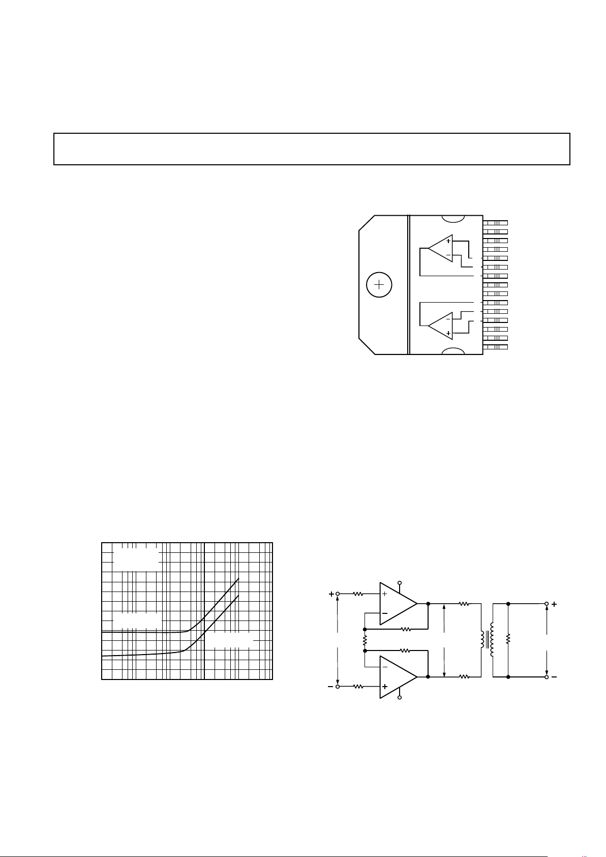
FUNCTIONAL BLOCK DIAGRAM
15-Lead Through-Hole SIP (Y) and Surface-Mount
DDPAK(VR)
NC
NC
NC
+IN1
–IN1
OUT1
–V
S
+V
S
OUT2
–IN2
+IN2
NC
NC
NC
NC
1
2
3
4
5
6
7
8
9
15
11
12
13
14
10
AD815
TAB IS
+V
S
NC = NO CONNECT
REFER TO PAGE 3 FOR 24-LEAD SOIC PACKAGE
REV. B
Information furnished by Analog Devices is believed to be accurate and
reliable. However, no responsibility is assumed by Analog Devices for its
use, nor for any infringements of patents or other rights of third parties
which may result from its use. No license is granted by implication or
otherwise under any patent or patent rights of Analog Devices.
a
High Output Current
Differential Driver
AD815
PRODUCT DESCRIPTION
The AD815 consists of two high speed amplifiers capable of
supplying a minimum of 500 mA. They are typically configured
as a differential driver enabling an output signal of 40 V p-p on
±15 V supplies. This can be increased further with the use of a
FEATURES
Flexible Configuration
Differential Input and Output Driver
or Two Single-Ended Drivers
High Output Power
Power Package
26 dBm Differential Line Drive for ADSL Application
40 V p-p Differential Output Voltage, R
L
= 50 ⍀
500 mA Minimum Output Drive/Amp, R
L
= 5 ⍀
Thermally Enhanced SOIC
400 mA Minimum Output Drive/Amp, R
L
= 10 ⍀
Low Distortion
–66 dB @ 1 MHz THD, R
L
= 200 ⍀, V
OUT
= 40 V p-p
0.05% and 0.45ⴗ Differential Gain and Phase, R
L
= 25 ⍀
(6 Back-Terminated Video Loads)
High Speed
120 MHz Bandwidth (–3 dB)
900 V/s Differential Slew Rate
70 ns Settling Time to 0.1%
Thermal Shutdown
APPLICATIONS
ADSL, HDSL and VDSL Line Interface Driver
Coil or Transformer Driver
CRT Convergence and Astigmatism Adjustment
Video Distribution Amp
Twisted Pair Cable Driver
FREQUENCY – Hz
–40
–50
–110
100 10M1k
TOTAL HARMONIC DISTORTION – dBc
10k 100k 1M
–60
–70
–80
–90
–100
VS = 615V
G = +10
V
OUT
= 40V p-p
RL = 50V
(DIFFERENTIAL)
RL = 200V
(DIFFERENTIAL)
Total Harmonic Distortion vs. Frequency
AMP1
+15V
–15V
R
L
120V
110V
499V
V
OUT
=
40Vp-p
V
IN
=
4Vp-p
1/2
AD815
1/2
AD815
G = +10
100V
100V
AMP2
VD =
40Vp-p
1:2
TRANSFORMER
R
1
= 15V
R2 = 15V
499V
Subscriber Line Differential Driver
coupling transformer with a greater than 1:1 turns ratio. The
low harmonic distortion of –66 dB @ 1 MHz into 200 Ω
combined with the wide bandwidth and high current drive make
the differential driver ideal for communication applications such
as subscriber line interfaces for ADSL, HDSL and VDSL.
The AD815 differential slew rate of 900 V/µs and high load drive
are suitable for fast dynamic control of coils or transformers,
and the video performance of 0.05% and 0.45° differential gain
and phase into a load of 25 Ω enable up to 12 back-terminated
loads to be driven.
Three package styles are available, and all work over the
industrial temperature range (–40°C to +85°C). Maximum
output power is achieved with the power package available for
through-hole mounting (Y) and surface-mounting (VR). The
24-lead SOIC (RB) is capable of driving 26 dBm for full rate
ADSL with proper heat sinking.
One Technology Way, P.O. Box 9106, Norwood, MA 02062-9106, U.S.A.
Tel: 781/329-4700 World Wide Web Site: http://www.analog.com
Fax: 781/326-8703 © Analog Devices, Inc., 1999
Page 2

AD815–SPECIFICATIONS
AD815A
Model Conditions V
S
Min Typ Max Units
DYNAMIC PERFORMANCE
Small Signal Bandwidth (–3 dB) G = +1 ±15 100 120 MHz
G = +1 ±5 90 110 MHz
Bandwidth (0.1 dB) G = +2 ±15 40 MHz
G = +2 ±5 10 MHz
Differential Slew Rate V
OUT
= 20 V p-p, G = +2 ±15 800 900 V/µs
Settling Time to 0.1% 10 V Step, G = +2 ±15 70 ns
NOISE/HARMONIC PERFORMANCE
Total Harmonic Distortion f = 1 MHz, R
LOAD
= 200 Ω, V
OUT
= 40 V p-p ±15 –66 dBc
Input Voltage Noise f = 10
kHz, G = +2 (Single Ended) ±5, ±15 1.85 nV/√Hz
Input Current Noise (+I
IN
) f = 10 kHz, G = +2 ±5, ±15 1.8 pA/√Hz
Input Current Noise (–I
IN
) f = 10 kHz, G = +2 ±5, ±15 19 pA/√Hz
Differential Gain Error NTSC, G = +2, R
LOAD
= 25 Ω±15 0.05 %
Differential Phase Error NTSC, G = +2, R
LOAD
= 25 Ω±15 0.45 Degrees
DC PERFORMANCE
Input Offset Voltage ±558mV
±15 10 15 mV
T
MIN
– T
MAX
30 mV
Input Offset Voltage Drift 20 µV/°C
Differential Offset Voltage ±50.52mV
±15 0.5 4 mV
T
MIN
– T
MAX
5mV
Differential Offset Voltage Drift 10 µV/°C
–Input Bias Current ±5, ±15 10 90 µA
T
MIN
– T
MAX
150 µA
+Input Bias Current ±5, ±15 2 5 µA
T
MIN
– T
MAX
5 µA
Differential Input Bias Current ±5, ±15 10 75 µA
T
MIN
– T
MAX
100 µA
Open-Loop Transresistance ±5, ±15 1.0 5.0 MΩ
T
MIN
– T
MAX
0.5 MΩ
INPUT CHARACTERISTICS
Differential Input Resistance +Input ±15 7 MΩ
–Input 15 Ω
Differential Input Capacitance ±15 1.4 pF
Input Common-Mode Voltage Range ±15 13.5 ±V
±53.5±V
Common-Mode Rejection Ratio T
MIN
– T
MAX
±5, ±15 57 65 dB
Differential Common-Mode Rejection Ratio T
MIN
– T
MAX
±5, ±15 80 100 dB
OUTPUT CHARACTERISTICS
Voltage Swing Single Ended, R
LOAD
= 25 Ω±15 11.0 11.7 ±V
±5 1.1 1.8 ±V
Differential, R
LOAD
= 50 Ω±15 21 23 ±V
T
MIN
– T
MAX
±15 22.5 24.5 ±V
Output Current
1, 2
VR, Y R
LOAD
= 5 Ω±15 500 750 mA
±5 350 400 mA
RB-24 R
LOAD
= 10 Ω±15 400 500 mA
Short Circuit Current ±15 1.0 A
Output Resistance ±15 13 Ω
MATCHING CHARACTERISTICS
Crosstalk f = 1 MHz ±15 –65 dB
POWER SUPPLY
Operating Range
3
T
MIN
– T
MAX
±18 V
Quiescent Current ±52330mA
±15 30 40 mA
T
MIN
– T
MAX
±540mA
±15 55 mA
Power Supply Rejection Ratio T
MIN
– T
MAX
±5, ±15 –55 –66 dB
NOTES
1
Output current is limited in the 24-lead SOIC package to the maximum power dissipation. See absolute maximum ratings and derating curves.
2
See Figure 12 for bandwidth, gain, output drive recommended operation range.
3
Observe derating curves for maximum junction temperature.
Specifications subject to change without notice.
REV. B–2–
(@ TA = +25ⴗC, VS = ⴞ15 V dc, RFB = 1 k⍀ and R
LOAD
= 100 ⍀ unless otherwise noted)
Page 3
AD815
REV. B –3–
MAXIMUM POWER DISSIPATION
The maximum power that can be safely dissipated by the AD815
is limited by the associated rise in junction temperature. The
maximum safe junction temperature for the plastic encapsulated
parts is determined by the glass transition temperature of the
plastic, about 150°C. Exceeding this limit temporarily may
cause a shift in parametric performance due to a change in the
stresses exerted on the die by the package. Exceeding a junction
temperature of 175°C for an extended period can result in
device failure.
The AD815 has thermal shutdown protection, which guarantees
that the maximum junction temperature of the die remains below a
safe level, even when the output is shorted to ground. Shorting
the output to either power supply will result in device failure.
To ensure proper operation, it is important to observe the
derating curves and refer to the section on power considerations.
It must also be noted that in high (noninverting) gain configurations
(with low values of gain resistor), a high level of input overdrive
can result in a large input error current, which may result in a
significant power dissipation in the input stage. This power
must be included when computing the junction temperature rise
due to total internal power.
AMBIENT TEMPERATURE – 8C
14
7
4
–50 90–40
MAXIMUM POWER DISSIPATION – Watts
–30 –20 –10 10 20 30 40 50 60 70 80
13
8
6
5
11
9
12
10
0
TJ = 1508C
3
2
1
0
AD815 AVR, AY
θ
JA
= 418C/W
(STILL AIR = 0FT/MIN)
NO HEAT SINK
θ
JA
= 528C/W
(STILL AIR = 0 FT/MIN)
NO HEAT SINK
AD815ARB-24
θ
JA
= 168C/W
SOLDERED DOWN TO
COPPER HEAT SINK
(STILL AIR = 0FT/MIN)
AD815 AVR, AY
Plot of Maximum Power Dissipation vs. Temperature
ABSOLUTE MAXIMUM RATINGS
1
Supply Voltage . . . . . . . . . . . . . . . . . . . . . . . . . . . ±18 V Total
Internal Power Dissipation
2
Plastic (Y and VR) . . 3.05 Watts (Observe Derating Curves)
Small Outline (RB) . . 2.4 Watts (Observe Derating Curves)
Input Voltage (Common Mode) . . . . . . . . . . . . . . . . . . . . ±V
S
Differential Input Voltage . . . . . . . . . . . . . . . . . . . . . . . . ±6 V
Output Short Circuit Duration
. . . . . . . . . . . . . . . . . . . . . . Observe Power Derating Curves
Can Only Short to Ground
Storage Temperature Range
Y, VR and RB Package . . . . . . . . . . . . . . . –65°C to +125°C
Operating Temperature Range
AD815A . . . . . . . . . . . . . . . . . . . . . . . . . . . –40°C to +85°C
Lead Temperature Range (Soldering, 10 sec) . . . . . . . +300°C
NOTES
1
Stresses above those listed under Absolute Maximum Ratings may cause perma-
nent damage to the device. This is a stress rating only; functional operation of the
device at these or any other conditions above those indicated in the operational
section of this specification is not implied. Exposure to absolute maximum rating
conditions for extended periods may affect device reliability.
2
Specification is for device in free air with 0 ft/min air flow: 15-Lead Through-Hole
and Surface Mount: θJA = 41°C/W; 24-Lead Surface Mount: θJA = 52°C/W.
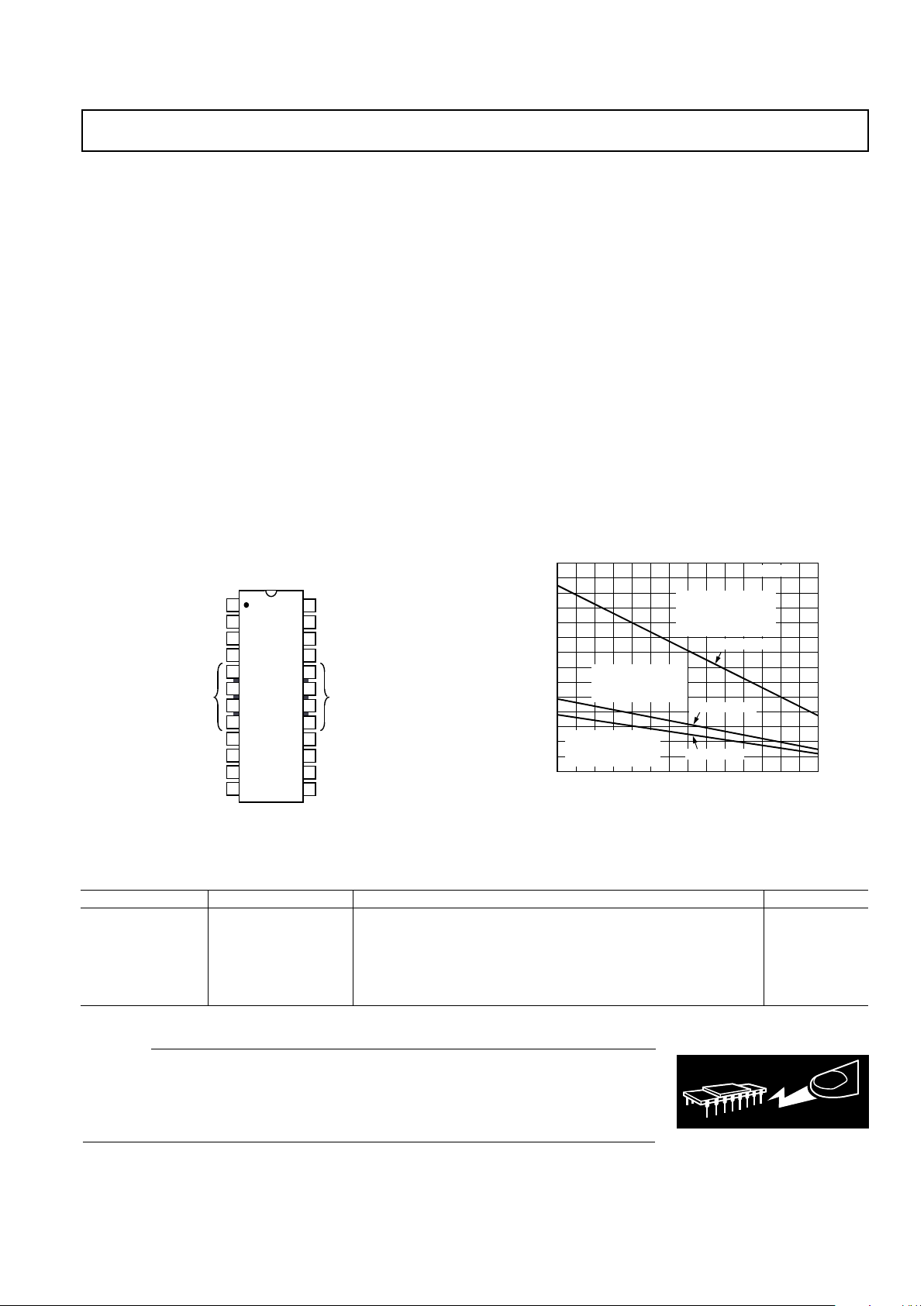
PIN CONFIGURATION
24-Lead Thermally-Enhanced SOIC (RB-24)
TOP VIEW
(Not to Scale)
AD815
13
16
15
14
24
23
22
21
20
19
18
17
12
11
10
9
8
1
2
3
4
7
6
5
NC = NO CONNECT
NC
NC
NC
NC
NC
NC
NC
NC
+IN1
–IN1
–IN2
+IN2
OUT1
–V
S
OUT2
+V
S
*HEAT TABS ARE CONNECTED TO THE POSITIVE SUPPLY.
THERMAL
HEAT TABS
+V
S
*
THERMAL
HEAT TABS
+V
S
*
ORDERING GUIDE
Model Temperature Range Package Description Package Option
AD815ARB-24 –40°C to +85°C 24-Lead Thermally Enhanced SOIC RB-24
AD815ARB-24-REEL –40°C to +85°C 24-Lead Thermally Enhanced SOIC RB-24
AD815AVR –40°C to +85°C 15-Lead Surface Mount DDPAK VR-15
AD815AY –40°C to +85°C 15-Lead Through-Hole SIP with Staggered Leads and 90° Lead Form Y-15
AD815AYS –40°C to +85°C 15-Lead Through-Hole SIP with Staggered Leads and Straight Lead Form YS-15
AD815-EB Evaluation Board
CAUTION
ESD (electrostatic discharge) sensitive device. Electrostatic charges as high as 4000 V readily
accumulate on the human body and test equipment and can discharge without detection.
Although the AD815 features proprietary ESD protection circuitry, permanent damage may
occur on devices subjected to high energy electrostatic discharges. Therefore, proper ESD
precautions are recommended to avoid performance degradation or loss of functionality.
WARNING!
ESD SENSITIVE DEVICE
Page 4
AD815
REV. B–4–
AD815–Typical Performance Characteristics
JUNCTION TEMPERATURE – 8C
–40 100–20020406080
36
34
18
SUPPLY CURRENT – mA
26
24
22
20
30
28
32
VS = 615V
VS = 65V
Figure 4. Total Supply Current vs. Temperature
SUPPLY VOLTAGE – 6Volts
33
30
18
0162
TOTAL SUPPLY CURRENT – mA
468101214
27
24
21
TA = +258C
Figure 5. Total Supply Current vs. Supply Voltage
JUNCTION TEMPERATURE – 8C
–40 100–20 0 20 40 60 80
10
0
–80
INPUT BIAS CURRENT – mA
–40
–50
–60
–70
–20
–30
–10
SIDE B
SIDE A
SIDE A, B
+I
B
–I
B
–I
B
SIDE A
SIDE B
VS = 615V, 65V
VS = 65V
VS = 615V
Figure 6. Input Bias Current vs. Temperature
SUPPLY VOLTAGE – 6Volts
20
15
0
0205
COMMON-MODE VOLTAGE RANGE – 6Volts
10 15
10
5
Figure 1. Input Common-Mode Voltage Range vs. Supply
Voltage
SUPPLY VOLTAGE – 6Volts
40
30
0
02051015
20
10
80
60
0
40
20
NO LOAD
RL = 50V
(DIFFERENTIAL)
RL = 25V
(SINGLE-ENDED)
SINGLE-ENDED OUTPUT VOLTAGE – V p-p
DIFFERENTIAL OUTPUT VOLTAGE – V p-p
Figure 2. Output Voltage Swing vs. Supply Voltage
LOAD RESISTANCE – (Differential – V) (Single-Ended – V/2)
30
25
0
10 10k100 1k
20
15
10
5
DIFFERENTIAL OUTPUT VOLTAGE – Volts p-p
60
50
0
40
30
20
10
VS = 615V
VS = 65V
SINGLE-ENDED OUTPUT VOLTAGE – Volts p-p
Figure 3. Output Voltage Swing vs. Load Resistance
Page 5
AD815
REV. B –5–
JUNCTION TEMPERATURE – 8C
0
–14
–40 100–20
INPUT OFFSET VOLTAGE – mV
020406080
–2
–6
–8
–10
–12
–4
VS = 65V
VS = 615V
Figure 7. Input Offset Voltage vs. Temperature
JUNCTION TEMPERATURE – 8C
750
600
450
–60 140–40
SHORT CIRCUIT CURRENT – mA
–20 0 2 0 40 60 80 100 120
700
650
550
500
VS = 615V
SINK
SOURCE
Figure 8. Short Circuit Current vs. Temperature
V
OUT
– Volts
15
0
–15
–20 20–16 –12 –8 –4 0 4 8 12 16
10
5
–5
–10
VS = 610V
VS = 65V
RTI OFFSET – mV
VS = 615V
TA = 258C
R
L
= 25V
1kV
1kV
R
L
=
25V
V
OUT
1/2
AD815
100V
49.9V
V
IN
f = 0.1Hz
Figure 9. Gain Nonlinearity vs. Output Voltage
LOAD CURRENT – Amps
80
0
–60
40
20
–20
–40
60
–2.0 2.0–1.6 –1.2 –0.8 –0.4
0
0.4 0.8 1.2 1.6
VS =
610V
VS =
65V
RTI OFFSET – mV
VS =
615V
TA = 258C
1kV
1kV
R
L
=
5V
V
OUT
1/2
AD815
100V
49.9V
V
IN
f = 0.1Hz
Figure 10. Thermal Nonlinearity vs. Output Current Drive
FREQUENCY – Hz
100
30k 300M100k
CLOSED-LOOP OUTPUT RESISTANCE – V
1M 10M 100M
10
1
0.1
0.01
300k 3M 30M
VS = 65V
VS = 615V
Figure 11. Closed-Loop Output Resistance vs. Frequency
FREQUENCY – MHz
40
0
0146
DIFFERENTIAL OUTPUT VOLTAGE – V p-p
10
30
20
10
RL = 50V
RL = 25V
RL = 1V
24 8 12
RL = 100V
TA = 258C
V
S
= ±15V
Figure 12. Large Signal Frequency Response
Page 6

AD815
REV. B–6–
FREQUENCY – Hz
100
10
1
10 100k100 1k 10k
VOLTAGE NOISE – nV/√Hz
100
10
1
CURRENT NOISE – pA/√Hz
INVERTING INPUT
CURRENT NOISE
NONINVERTING INPUT
CURRENT NOISE
INPUT VOLTAGE
NOISE
Figure 13. Input Current and Voltage Noise vs. Frequency
FREQUENCY – Hz
90
80
10
10k 100M100k
COMMON-MODE REJECTION – dB
1M 10M
70
60
50
40
30
20
VS = 615V
SIDE A
SIDE B
562V
562V
562V
562V
V
OUTV
IN
1/2
AD815
Figure 14. Common-Mode Rejection vs. Frequency
FREQUENCY – MHz
0.01
0
–10
–20
–30
–40
–50
–60
–70
–80
–90
–100
0.1
PSRR – dB
1 10 100 300
–PSRR
+PSRR
VS = 615V
G = +2
R
L
= 100V
Figure 15. Power Supply Rejection vs. Frequency
FREQUENCY – Hz
100 100M1k
TRANSIMPEDANCE – dB
10k 100k 1M 10M
120
110
100
90
80
70
60
50
40
30
PHASE – Degrees
100
500
0
–50
–100
–150
–200
–250
TRANSIMPEDANCE
PHASE
Figure 16. Open-Loop Transimpedance vs. Frequency
FREQUENCY – Hz
–40
–50
–110
100 10M1k
TOTAL HARMONIC DISTORTION – dBc
10k 100k 1M
–60
–70
–80
–90
–100
VS = 615V
G = +10
V
OUT
= 40V p-p
RL = 50V
(DIFFERENTIAL)
RL = 200V
(DIFFERENTIAL)
Figure 17. Total Harmonic Distortion vs. Frequency
SETTLING TIME – ns
10
–10
8
2
–2
–6
–8
6
4
0
–4
60
OUTPUT SWING FROM ±V TO 0 – Volts
40 80 100
GAIN = +2
V
S
= 615V
1%
0.1%
020 70
1%
0.1%
Figure 18. Output Swing and Error vs. Settling Time
Page 7

AD815
REV. B –7–
OUTPUT STEP SIZE – V p-
p
700
0
600
500
400
300
200
100
0255101520
SINGLE-ENDED SLEW RATE – V/ms
(PER AMPLIFIER)
G = +2
G = +10
1400
0
1200
1000
800
600
400
200
DIFFERENTIAL SLEW RATE – V/
m
s
Figure 19. Slew Rate vs. Output Step Size
JUNCTION TEMPERATURE – 8C
–85
–80
–60
–40 100–20
PSRR – dB
020406080
–75
–70
–65
+PSRR
–PSRR
SIDE B
SIDE A
SIDE B
SIDE A
VS = 615V
Figure 20. PSRR vs. Temperature
JUNCTION TEMPERATURE – 8C
–40 100–20020406080
–74
–66
CMRR – dB
–73
–70
–69
–68
–67
–72
–71
–CMRR
+CMRR
Figure 21. CMRR vs. Temperature
JUNCTION TEMPERATURE – 8C
5
4
0
–40 100–20
OPEN-LOOP TRANSRESISTANCE – MV
020406080
3
2
1
+T
Z
SIDE A
SIDE B
SIDE A
SIDE B
–T
Z
Figure 22. Open-Loop Transresistance vs. Temperature
JUNCTION TEMPERATURE – 8C
15
14
10
–40 100–20
OUTPUT SWING – Volts
020406080
13
12
11
VS = 615V
| –V
OUT
|
+V
OUT
+V
OUT
| –V
OUT
|
RL = 150V
RL = 25V
Figure 23. Single-Ended Output Swing vs. Temperature
JUNCTION TEMPERATURE – 8C
27
26
22
25
24
23
–40 100–20
OUTPUT SWING – Volts
020406080
VS = 615V
RL = 50V
–V
OUT
+V
OUT
Figure 24. Differential Output Swing vs. Temperature
Page 8

AD815
REV. B–8–
0.04
0.03
0.02
0.01
0.00
–0.01
–0.02
–0.03
–0.04
DIFF GAIN – %
0.12
0.10
0.08
0.06
0.04
0.02
0.00
–0.02
–0.04
DIFF PHASE – De
g
rees
G = +2
R
F
= 1kV
NTSC
1234567891011
0.5
0.4
0.3
0.2
0.1
0.0
–0.1
–0.2
–0.3
GAIN
PHASE
0.005
0.000
–0.005
–0.010
–0.015
–0.020
–0.025
–0.030
0.010
DIFF GAIN – %
DIFF PHASE – Degrees
1234567891011
6 BACK TERMINATED LOADS (25V)
2 BACK TERMINATED LOADS (75V)
G = +2
R
F
= 1kV
NTSC
GAIN
PHASE
GAIN
PHASE
Figure 25. Differential Gain and Differential Phase
(per Amplifier)
FREQUENCY – MHz
0.03
–10
–20
–30
–40
–50
–60
–70
–80
–90
–100
0.1
CROSSTALK – dB
1 10 100 300
SIDE B
SIDE A
G = +2
R
F
= 499V
VS = 615V, 65V
V
IN
= 400mVrms
RL = 100V
–110
Figure 26. Output-to-Output Crosstalk vs. Frequency
FREQUENCY – MHz
1
0
–1
–2
–3
–4
–5
–6
–7
–9
2
0.1 3001
OUTPUT VOLTAGE – dB
10 100
SIDE B
SIDE A
562V
100V
100V
49.9V
V
OUT
V
IN
VS = 615V
V
IN
= 0 dBm
Figure 27. –3 dB Bandwidth vs. Frequency, G = +1
FREQUENCY – MHz
0.1
0
0.1 3001
NORMALIZED FLATNESS – dB
10 100
615V
65V
499V
100V
100V
49.9V
V
OUT
V
IN
499V
A
B
A
B
615V
65V
–0.1
–0.2
–0.3
–0.4
–0.5
–0.6
–0.7
1
0
–1
–2
–3
–4
–5
–6
–7
–8
–9
NORMALIZED FREQUENCY RESPONSE – dB
Figure 28. Bandwidth vs. Frequency, G = +2
FREQUENCY – MHz
0
0.1 3001
NORMALIZED OUTPUT VOLTAGE – dB
10 100
499V
100V
100V
V
OUT
V
IN
124V
SIDE A
SIDE B
–1
–2
–3
–4
–5
–6
–7
1
VS = 615V
49.9V
Figure 29. –3 dB Bandwidth vs. Frequency, G = +5
10
0%
100
90
1ms
5V
Figure 30. 40 V p-p Differential Sine Wave, RL = 50Ω,
f = 100 kHz
Page 9

AD815
REV. B –9–
1/2 AD815
0.1mF
10mF
+15V
562V
0.1mF
10mF
7
–15V
RL = 100V
100V
50V
V
IN
PULSE
GENERATOR
T
R/TF
= 250ps
8
Figure 31. Test Circuit, Gain = +1
100mV
20ns
SIDE B
SIDE A
G = +1
R
F
= 698V
R
L
= 100V
Figure 32. 500 mV Step Response, G = +1
1V
20ns
SIDE B
SIDE A
G = +1
R
F
= 562V
R
L
= 100V
Figure 33. 4 V Step Response, G = +1
2V
50ns
SIDE B
SIDE A
G = +1
R
F
= 562V
R
L
= 100V
Figure 34. 10 V Step Response, G = +1
1/2 AD815
8
0.1mF
10mF
+15V
0.1mF
10mF
7
–15V
RL = 100V
100V
50V
V
IN
PULSE
GENERATOR
TR/TF = 250ps
R
S
R
F
Figure 35. Test Circuit, Gain = 1 + RF/R
S
5V
100ns
SIDE B
SIDE A
G = +5
R
F
= 562V
R
L
= 100V
R
S
= 140V
Figure 36. 20 V Step Response, G = +5
1/2 AD815
8
0.1mF
10mF
+15V
0.1mF
10mF
7
–15V
RL = 100V
100V
55V
V
IN
PULSE
GENERATOR
T
R/TF
= 250ps
562V
562V
Figure 37. Test Circuit, Gain = –1
100mV
20ns
SIDE B
SIDE A
G = –1
R
F
= 562V
R
L
= 100V
Figure 38. 500 mV Step Response, G = –1
Page 10
AD815
REV. B–10–
Choice of Feedback and Gain Resistors
The fine scale gain flatness will, to some extent, vary with
feedback resistance. It therefore is recommended that once
optimum resistor values have been determined, 1% tolerance
values should be used if it is desired to maintain flatness over
a wide range of production lots. Table I shows optimum values
for several useful configurations. These should be used as
starting point in any application.
Table I. Resistor Values
RF (⍀)RG (⍀)
G = +1 562 ⬁
–1 499 499
+2 499 499
+5 499 125
+10 1 k 110
PRINTED CIRCUIT BOARD LAYOUT
CONSIDERATIONS
As to be expected for a wideband amplifier, PC board parasitics
can affect the overall closed-loop performance. Of concern are
stray capacitances at the output and the inverting input nodes. If
a ground plane is to be used on the same side of the board as
the signal traces, a space (5 mm min) should be left around the
signal lines to minimize coupling.
POWER SUPPLY BYPASSING
Adequate power supply bypassing can be critical when optimizing
the performance of a high frequency circuit. Inductance in the
power supply leads can form resonant circuits that produce
peaking in the amplifier’s response. In addition, if large current
transients must be delivered to the load, then bypass capacitors
(typically greater than 1 µF) will be required to provide the best
settling time and lowest distortion. A parallel combination of
10.0 µF and 0.1 µF is recommended. Under some low frequency
applications, a bypass capacitance of greater than 10 µF may be
necessary. Due to the large load currents delivered by the
AD815, special consideration must be given to careful bypassing.
The ground returns on both supply bypass capacitors as well as
signal common must be “star” connected as shown in Figure 41.
R
F
R
G
(OPTIONAL)
R
F
+V
S
+OUT
–OUT
–V
S
+IN
–IN
Figure 41. Signal Ground Connected in “Star”
Configuration
1V
20ns
SIDE B
SIDE A
G = –1
R
F
= 562V
R
L
= 100V
Figure 39. 4 V Step Response, G = –1
THEORY OF OPERATION
The AD815 is a dual current feedback amplifier with high
(500 mA) output current capability. Being a current feedback
amplifier, the AD815’s open-loop behavior is expressed
as transimpedance, ∆V
O
/∆I
–IN
, or TZ. The open-loop
transimpedance behaves just as the open-loop voltage gain
of a voltage feedback amplifier, that is, it has a large dc value
and decreases at roughly 6 dB/octave in frequency.
Since R
IN
is proportional to 1/gM, the equivalent voltage gain is
just T
Z
× g
M
, where the gM in question is the transconductance
of the input stage. Using this amplifier as a follower with gain,
Figure 40, basic analysis yields the following result:
V
O
V
IN
= G ×
T
Z
S
()
TZS
()
+G × RIN+ R
F
where:
G
R
R
F
G
=+1
RIN = 1/g
M
≈ 25 Ω
R
IN
V
IN
R
F
V
OUT
R
G
R
N
Figure 40. Current Feedback Amplifier Operation
Recognizing that G × R
IN
<< RF for low gains, it can be seen to
the first order that bandwidth for this amplifier is independent
of gain (G).
Considering that additional poles contribute excess phase at
high frequencies, there is a minimum feedback resistance below
which peaking or oscillation may result. This fact is used to
determine the optimum feedback resistance, R
F
. In practice
parasitic capacitance at the inverting input terminal will also add
phase in the feedback loop, so picking an optimum value for R
F
can be difficult.
Achieving and maintaining gain flatness of better than 0.1 dB at
frequencies above 10 MHz requires careful consideration of
several issues.
Page 11

AD815
REV. B –11–
DC ERRORS AND NOISE
There are three major noise and offset terms to consider in
a current feedback amplifier. For offset errors refer to the
equation below. For noise error the terms are root-sum-squared
to give a net output error. In the circuit below (Figure 42), they
are input offset (V
IO
) which appears at the output multiplied by
the noise gain of the circuit (1 + R
F/RG
), noninverting input
current (I
BN
× R
N
) also multiplied by the noise gain, and the
inverting input current, which when divided between R
F
and R
G
and subsequently multiplied by the noise gain always appear at
the output as I
BI
× R
F
. The input voltage noise of the AD815 is
less than 2 nV/√Hz. At low gains though, the inverting input
current noise times R
F
is the dominant noise source. Careful
layout and device matching contribute to better offset and
drift specifications for the AD815 compared to many other
current feedback amplifiers. The typical performance curves
in conjunction with the equations below can be used to predict
the performance of the AD815 in any application.
V
OUT
= VIO× 1 +
R
F
R
G
± I
BN
× RN× 1 +
R
F
R
G
± I
BI
× R
F
I
BI
I
BN
R
G
R
N
R
F
V
OUT
Figure 42. Output Offset Voltage
POWER CONSIDERATIONS
The 500 mA drive capability of the AD815 enables it to drive
a 50 Ω load at 40 V p-p when it is configured as a differential
driver. This implies a power dissipation, P
IN
, of nearly 5 watts.
To ensure reliability, the junction temperature of the AD815
should be maintained at less than 175°C. For this reason,
the AD815 will require some form of heat sinking in most
applications. The thermal diagram of Figure 43 gives the
basic relationship between junction temperature (T
J
) and
various components of θ
JA
.
TTP
AINAJJ
=+ θ
Equation 1
θA
(JUNCTION TO
DIE MOUNT)
θ
B
(DIE MOUNT
TO CASE)
θ
A
+ θB = θ
JC
CASE
T
A
T
J
θ
JC
θ
CA
T
A
θ
JA
T
J
P
IN
WHERE:
P
IN
= DEVICE DISSIPATION
T
A
= AMBIENT TEMPERATURE
T
J
= JUNCTION TEMPERATURE
θ
JC
= THERMAL RESISTANCE – JUNCTION TO CASE
θ
CA
= THERMAL RESISTANCE – CASE TO AMBIENT
Figure 43. A Breakdown of Various Package Thermal
Resistances
Figure 44 gives the relationship between output voltage swing
into various loads and the power dissipated by the AD815 (P
IN
).
This data is given for both sine wave and square wave (worst
case) conditions. It should be noted that these graphs are for
mostly resistive (phase < ±10°) loads. When the power dissipation
requirements are known, Equation 1 and the graph on Figure 45
can be used to choose an appropriate heat sinking configuration.
4
3
P
IN
– Watts
10 20 30 40
2
1
V
OUT
– Volts p-p
RL = 50V
RL = 100V
RL = 200V
f = 1kHz
SQUARE WAVE
SINE WAVE
Figure 44. Total Power Dissipation vs. Differential Output
Voltage
Normally, the AD815 will be soldered directly to a copper pad.
Figure 45 plots θ
JA
against size of copper pad. This data pertains
to copper pads on both sides of G10 epoxy glass board connected
together with a grid of feedthroughs on 5 mm centers.
This data shows that loads of 100 ohms or less will usually not
require any more than this. This is a feature of the AD815’s
15-lead power SIP package.
An important component of θ
JA
is the thermal resistance of the
package to heatsink. The data given is for a direct soldered
connection of package to copper pad. The use of heatsink
grease either with or without an insulating washer will increase
this number. Several options now exist for dry thermal connections. These are available from Bergquist as part # SP600-90.
Consult with the manufacturer of these products for details of
their application.
COPPER HEAT SINK AREA (TOP AND BOTTOM) – mm
2
35
30
10
0 2.5k0.5k
θ
JA
– 8C/W
1k 1.5k 2k
25
20
15
AD815AVR, AY (θJC = 28C/W)
Figure 45. Power Package Thermal Resistance vs. Heat
Sink Area
Page 12

AD815
REV. B–12–
Other Power Considerations
There are additional power considerations applicable to the
AD815. First, as with many current feedback amplifiers, there is an
increase in supply current when delivering a large peak-to-peak
voltage to a resistive load at high frequencies. This behavior is
affected by the load present at the amplifier’s output. Figure 12
summarizes the full power response capabilities of the AD815.
These curves apply to the differential driver applications (e.g.,
Figure 49 or Figure 53). In Figure 12, maximum continuous
peak-to-peak output voltage is plotted vs. frequency for various
resistive loads. Exceeding this value on a continuous basis can
damage the AD815.
The AD815 is equipped with a thermal shutdown circuit. This
circuit ensures that the temperature of the AD815 die remains
below a safe level. In normal operation, the circuit shuts down
the AD815 at approximately 180°C and allows the circuit to
turn back on at approximately 140°C. This built-in hysteresis
means that a sustained thermal overload will cycle between
power-on and power-off conditions. The thermal cycling
typically occurs at a rate of 1 ms to several seconds, depending
on the power dissipation and the thermal time constants of the
package and heat sinking. Figures 46 and 47 illustrate the
thermal shutdown operation after driving OUT1 to the + rail,
and OUT2 to the – rail, and then short-circuiting to ground
each output of the AD815. The AD815 will not be damaged by
momentary operation in this state, but the overload condition
should be removed.
10
0%
100
90
OUT 1
200ms5V
OUT 2
Figure 46. OUT2 Shorted to Ground, Square Wave Is
OUT1, R
F
= 1 kΩ, RG = 222
Ω
10
0%
100
90
OUT 1
5ms5V
OUT 2
Figure 47. OUT1 Shorted to Ground, Square Wave Is
OUT2, R
F
= 1 kΩ, RG = 222
Ω
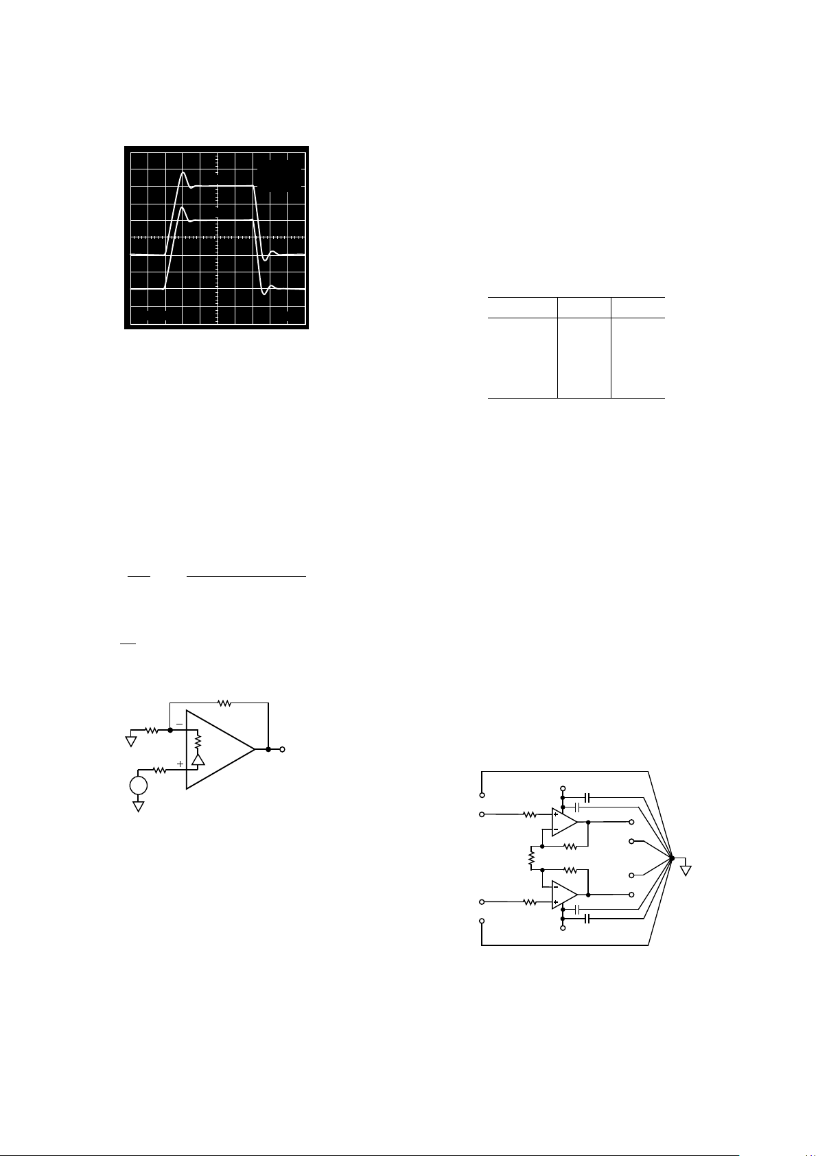
Parallel Operation
To increase the drive current to a load, both of the amplifiers
within the AD815 can be connected in parallel. Each amplifier
should be set for the same gain and driven with the same signal.
In order to ensure that the two amplifiers share current, a small
resistor should be placed in series with each output. See Figure
48. This circuit can deliver 800 mA into loads of up to 12.5 Ω.
6
4
5
8
+15V
499V 499V
1V
10
7
–15V
499V 499V
1V
R
L
9
11
50V
0.1mF
10mF
0.1mF
10mF
1/2
AD815
1/2
AD815
100V
100V
Figure 48. Parallel Operation for High Current Output
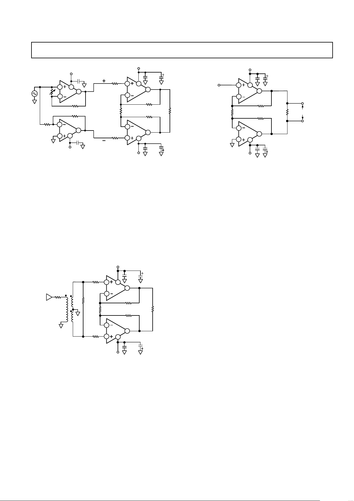
Differential Operation
Various circuit configurations can be used for differential
operation of the AD815. If a differential drive signal is available, the two halves can be used in a classic instrumentation
configuration to provide a circuit with differential input and
output. The circuit in Figure 49 is an illustration of this. With
the resistors shown, the gain of the circuit is 11. The gain can
be changed by changing the value of R
G
. This circuit, however,
provides no common-mode rejection.
6
4
5
8
+15V
10
7
–15V
R
F
499V
R
L
9
11
0.1mF
10mF
R
G
100V
R
F
499V
0.1mF
10mF
1/2
AD815
V
OUT
V
IN
1/2
AD815
100V
100V
+IN
–IN
OUT 1
OUT 2
Figure 49. Fully-Differential Operation
Creating Differential Signals
If only a single ended signal is available to drive the AD815 and
a differential output signal is desired, several circuits can be
used to perform the single-ended-to-differential conversion.
One circuit to perform this is to use a dual op amp as a
predriver that is configured as a noninverter and inverter. The
circuit shown in Figure 50 performs this function. It uses an
AD826 dual op amp with the gain of one amplifier set at +1 and
the gain of the other at –1. The 1 kΩ resistor across the input
terminals of the follower makes the noise gain (NG = 1) equal
to the inverter’s. The two outputs then differentially drive the
inputs to the AD815 with no common-mode signal to first order.
Page 13
AD815
REV. B –13–
6
458
+15V
10
7
–15V
R
F
499V
R
L
9
11
0.1mF
10mF
R
G
100V
R
F
499V
0.1mF
10mF
1/2
AD815
1
8
+15V
0.1mF
2
1kV
4
–15V
1kV
7
0.1mF
6
5
1kV
3
1/2
AD815
1/2
AD826
1/2
AD826
100V
100V
1kV
Figure 50. Differential Driver with Single-Ended
Differential Converter
Another means for creating a differential signal from a singleended signal is to use a transformer with a center-tapped
secondary. The center tap of the transformer is grounded and
the two secondary windings are connected to obtain opposite
polarity signals to the two inputs of the AD815 amplifiers. The
bias currents for the AD815 inputs are provided by the center
tap ground connection through the transformer windings.
One advantage of using a transformer is its ability to provide
isolation between circuit sections and to provide good commonmode rejection. The disadvantages are that transformers have
no dc response and can sometimes be large, heavy, and expensive.
This circuit is shown in Figure 51.
6
458
+15V
10
7
–15V
R
L
9
11
0.1mF
10mF
200V
0.1mF
10mF
1/2
AD815
1kV
1kV
1/2
AD815
50V
100V
100V
50V
Figure 51. Differential Driver with Transformer Input
Direct Single-Ended-to-Differential Conversion
Two types of circuits can create a differential output signal from
a single-ended input without the use of any other components
than resistors. The first of these is illustrated in Figure 52.
6
458
+15V
10
7
–15V
R
F1
402V
R
L
9
11
R
G
100V
R
F2
499V
1/2
AD815
1/2
AD815
V
IN
V
OUT
AMP 1
AMP 2
Figure 52. Direct Single-Ended-to-Differential Conversion
Amp 1 has its + input driven with the input signal, while the
+ input of Amp 2 is grounded. Thus the – input of Amp 2 is
driven to virtual ground potential by its output. Therefore
Amp 1 is configured for a noninverting gain of five, (1 + R
F1/RG
),
because R
G
is connected to the virtual ground of Amp 2’s – input.
When the + input of Amp 1 is driven with a signal, the same
signal appears at the – input of Amp 1. This signal serves as an
input to Amp 2 configured for a gain of –5, (–R
F2/RG
). Thus the
two outputs move in opposite directions with the same gain and
create a balanced differential signal.
This circuit can work at various gains with proper resistor
selection. But in general, in order to change the gain of the
circuit, at least two resistor values will have to be changed. In
addition, the noise gain of the two op amps in this configuration
will always be different by one, so the bandwidths will not match.
A second circuit that has none of the disadvantages mentioned
in the above circuit creates a differential output voltage feedback
op amp out of the pair of current feedback op amps in the AD815.
This circuit, drawn in Figure 53, can be used as a high power
differential line driver, such as required for ADSL (asymmetrical
digital subscriber loop) line driving.
Each of the AD815’s op amps is configured as a unity gain
follower by the feedback resistors (R
A
). Each op amp output
also drives the other as a unity gain inverter via the two R
B
s,
creating a totally symmetrical circuit.
If the + input to Amp 2 is grounded and a small positive signal
is applied to the + input of Amp 1, the output of Amp 1 will be
driven to saturation in the positive direction and the output of
Amp 2 driven to saturation in the negative direction. This is
similar to the way a conventional op amp behaves without any
feedback.
Page 14

AD815
REV. B–14–
6
458
10
7
–15V
R
A
499V
9
11
0.1mF
10mF
0.1mF
10mF
AMP1
AMP2
V
IN
+15V
V
CC
R
F
499V
~20pF
R
B
499V
R
A
499V
R
B
499V
V
CC
250
(50V)
(OPTIONAL)
R
I
499V
50V
50V
(OPTIONAL)
100V
1/2
AD815
1/2
AD815
Figure 53. Single-Ended-to-Differential Driver
If a resistor (RF) is connected from the output of Amp 2 to the
+ input of Amp 1, negative feedback is provided which closes
the loop. An input resistor (R
I
) will make the circuit look like a
conventional inverting op amp configuration with differential
outputs. The inverting input to this dual output op amp becomes
Pin 4, the positive input of Amp 1.
The gain of this circuit from input to either output will be ± R
F
/
R
I
. Or the single-ended-to-differential gain will be 2 × R
F/RI.
The differential outputs can be applied to the primary of a
transformer. If each output can swing ±10 V, the effective swing
on the transformer primary is 40 V p-p. The optional capacitor
can be added to prevent any dc current in the transformer due
to dc offsets at the output of the AD815.
Figure 55. AD815 Evaluation Board Schematic
Figure 54. AD815 Video Distribution Amp Driving
12 Video Cables
Twelve Channel Video Distribution Amplifier
The high current of the AD815 enables it to drive up to twelve
standard 75 Ω reverse terminated video loads. Figure 54 is a
schematic of such an application.
The input video signal is terminated in 75 Ω and applied to the
noninverting inputs of both amplifiers of the AD815. Each
amplifier is configured for a gain of two to compensate for the
divide-by-two feature of each cable termination. Six separate
75 Ω resistors for each amplifier output are used for the cable
back termination. In this manner, all cables are relatively
independent of each other and small disturbances on any cable
will not have an effect on the other cables.
When driving six video cables in this fashion, the load seen by
each amplifier output is resistive and is equal to 150 Ω/6 or
25 Ω. The differential gain is 0.05% and the differential phase
is 0.45°.
4
5
1/2
AD815
C2
0.1mF
C3
10mF
TP2
+15V
R10
R21
R18
R12
R9
J3
J6R13
C10
0.1mF
C11
10mF
TP1
–15V
U1
R11
C13 R16
R15
U1
R6
R17
TP4 TP3
+15V
–15V
B2
B1
B3
C9
JP1
R20
J4
1
2
3
T1
J5
C1
R3
R7
R2
R4
J1
R5
R19
R1
R14
R8
2
1
10
9
R22
4
7
5
6
11
12
8
8
6
1
2
3
J2
J7
1
2
3
C6
11
10
7
9
1/2
AD815
6
+15V
8
7
–15V
9
11
0.1mF10mF
10
5
4
100V
100V
75V
VIDEO IN
499V
0.1mF
10mF
499V
499V
499V
12 3 75V
12 3
VIDEO OUT
TO 75V
CABLES
AD815
Page 15

AD815
REV. B –15–
Figure 56. AD815 AVR Evaluation Board Assembly Drawing
Figure 57. AD815 AVR Evaluation Board Layout
(Component Side)
Figure 58. AD815 AVR Evaluation Board Layout
(Solder Side)
Page 16

AD815
REV. B–16–
C2106a–0–12/99
PRINTED IN U.S.A.
15-Lead Surface Mount DDPAK
(VR-15)
1
0.694 (17.63)
0.684 (17.37)
0.080 (2.03)
0.065 (1.65)
2 PLACES
0.516
(13.106)
0.110
(2.79)
BSC
0.042
(1.066)
TYP
0.137
(3.479)
TYP
0.394
(10.007)
0.152 (3.86)
0.148 (3.76)
0.600 (15.24)
BSC
0.079 (2.006)
DIA
2 PLACES
15
0.024 (0.61)
0.014 (0.36)
0.063 (1.60)
0.057 (1.45)
8°
0°
0.088 (2.24)
0.068 (1.72)
0.426 (10.82)
0.416 (10.57)
SEATING
PLANE
0.031 (0.79)
0.024 (0.60)
0.100 (2.54)
BSC
0.798 (20.27)
0.778 (19.76)
0.182 (4.62)
0.172 (4.37)
0.146 (3.70)
0.138 (3.50)
PIN 1
15-Lead Through-Hole SIP with Staggered Leads and
90ⴗ Lead Form (Y-15)
0.063 (1.60)
0.057 (1.45)
0.671
±0.006
(17.043
±0.152)
SHORT
LEAD
0.024 (0.61)
0.014 (0.36)
0.666
±0.006
(16.916
±0.152)
LONG
LEAD
0.691 ±0.010
(17.551 ±0.254)
0.766 ±0.010
(19.456 ±0.254)
0.791 ±0.010
(20.091 ±0.254)
0.694 (17.63)
0.684 (17.37)
PIN 1
0.110
(2.79)
BSC
0.394
(10.007)
0.152 (3.86)
0.148 (3.76)
0.080 (2.03)
0.065 (1.65)
2 PLACES
0.516 (13.106)
0.042
(1.066)
TYP
0.137
(3.479)
TYP
0.079 (2.006)
DIA
2 PLACES
0.426 (10.82)
0.416 (10.57)
1 15
0.700 (17.78) BSC
SEATING
PLANE
0.031 (0.79)
0.024 (0.60)
0.050
(1.27)
BSC
0.798 (20.27)
0.778 (19.76)
0.182 (4.62)
0.172 (4.37)
0.209 ±0.010
(5.308 ±0.254)
OUTLINE DIMENSIONS
Dimensions shown in inches and (mm).
24-Lead Thermally Enhanced SOIC
(RB-24)
24 13
121
0.6141 (15.60)
0.5985 (15.20)
0.4193 (10.65)
0.3937 (10.00)
0.2992 (7.60)
0.2914 (7.40)
PIN 1
SEATING
PLANE
0.0118 (0.30)
0.0040 (0.10)
0.0201 (0.51)
0.0130 (0.33)
0.1043 (2.65)
0.0926 (2.35)
0.0500
(1.27)
BSC
0.0125 (0.32)
0.0091 (0.23)
0.0500 (1.27)
0.0157 (0.40)
8°
0°
0.0291 (0.74)
0.0098 (0.25)
x 45°
15-Lead Through-Hole SIP with Staggered Leads and
Straight Lead Form (YS-15)
0.080 (2.03)
0.065 (1.65)
2 PLACES
0.694 (17.63)
0.684 (17.37)
PIN 1
0.110
(2.79)
BSC
0.042
(1.07)
TYP
0.137
(3.48)
TYP
0.394
(10.007)
0.152 (3.86)
0.148 (3.76)
0.700 (17.78) BSC
0.079
(2.007) DIA
2 PLACES
0.426 (10.82)
0.416 (10.57)
0.516 (13.106)
1 15
0.063 (1.60)
0.057 (1.45)
0.627
±0.010
(15.926
±0.254)
SHORT
LEAD
0.601
±0.010
(15.265
±0.254)
LONG
LEAD
0.176 (4.47)
0.150 (3.81)
0.710 (18.03)
0.690 (17.53)
0.200
(5.08)
BSC
0.169
(4.29)
BSC
0.024 (0.61)
0.014 (0.36)
0.031 (0.79)
0.024 (0.60)
0.050 (1.27)
BSC
0.798 (20.27)
0.778 (19.76)
0.182 (4.62)
0.172 (4.37)
SEATING
PLANE
 Loading...