

Page 1
High Speed, Triple Differential Receiver
G
www.BDTIC.com/ADI
FEATURES
High speed: 500 MHz, 2000 V/μs @ G = 1, VO = 2 V p-p
0.1 dB flatness out to 75 MHz
High CMRR: 69 dB @ 10 MHz
High differential input impedance: 1 MΩ
Wide input common-mode range: ± 3.8 V (±5 V supplies)
On-chip gain-setting resistors
C
an be configured for gain of 1 or 2
Fast settling: 15 ns to 0.1% @ 2 V p-p
Low input referred noise: 13nV/√Hz
Disable feature
Small packaging: 32-lead, 5 mm × 5 mm LFCSP
APPLICATIONS
RGB video receivers
YPbPr video receivers
KVM (keyboard, video, mouse)
UTP (unshielded twisted pair) receivers
GND
REF_G
AIN_G
IN+_G
IN–_G
REF_R
GAIN_R
GND
with Comparators
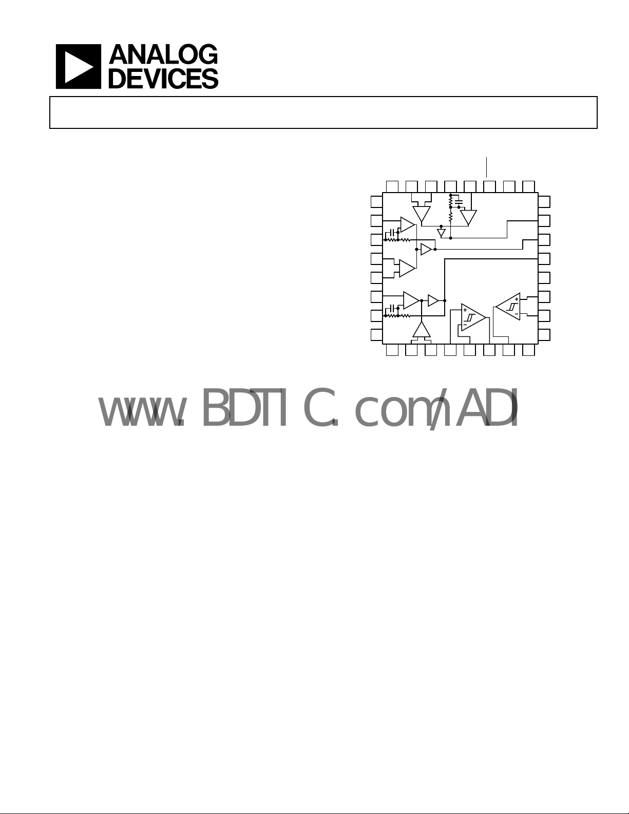
FUNCTIONAL BLOCK DIAGRAM
DIS/PD
REF_B
GAIN_B
IN+_B
IN–_B
GND
C
1
2
+
C
–
3
RR
4
+
–
5
6
+
C
–
7
RR
8
9 10111213141516
GND
R
+
–
+
–
R
AD8145
B
A
–
+
IN–_R
IN+_R
AD8145
S–
GND
V
2526272829303132
24
GND
23
OUT_B
22
OUT_G
21
OUT_R
20
V
19
COMPB_IN+
18
COMPB_IN–
17
GND
GND
S+
GENERAL DESCRIPTION
The AD8145 is a triple, low cost, differential-to-single-ended
receiver specifically designed for receiving red-green-blue
(RGB) video signals over twisted pair cable or differential
printed circuit board traces. It can also be used to receive any
type of analog signal or high speed data transmission. Two
auxiliary comparators with hysteresis are provided, which can
be used to decode video sync signals that are encoded on the
received common-mode voltages, to receive digital signals, or as
general-purpose comparators. The AD8145 can be used in
conjunction with the
ivers to provide a complete low cost solution for RGB over
dr
Category 5 UTP cable applications, including KVM.
The excellent common-mode rejection (69 dB @ 10 MHz) of
e AD8145 allows for the use of low cost, unshielded twisted
th
pair cables in noisy environments.
AD8133 or AD8134 triple differential
COMPA_IN–
COMPA_IN+
COMPB_OUT
COMPA_OUT
Figure 1.
The AD8145 can be configured for a differential-to-single-
d gain of 1 or 2 by connecting the GAIN pin of each
ende
channel to its respective output (G = 1) or connecting it to a
reference voltage (G = 2), which is normally grounded.
A REF input is provided on each channel that allows designers
to
level shift the output signals.
The AD8145 is available in a 5 mm × 5 mm, 32-lead LFCSP and
ted to work over the extended industrial temperature range
is ra
of −40°C to +105°C.
6307-001
Rev. 0
Information furnished by Analog Devices is believed to be accurate and reliable. However, no
responsibility is assumed by Anal og Devices for its use, nor for any infringements of patents or ot her
rights of third parties that may result from its use. Specifications subject to change without notice. No
license is granted by implication or otherwise under any patent or patent rights of Analog Devices.
Trademarks and registered trademarks are the property of their respective owners.
One Technology Way, P.O. Box 9106, Norwood, MA 02062-9106, U.S.A.
Tel: 781.329.4700 www.analog.com
Fax: 781.461.3113 ©2006 Analog Devices, Inc. All rights reserved.
Page 2

AD8145
www.BDTIC.com/ADI
TABLE OF CONTENTS
Features.............................................................................................. 1
Applications....................................................................................... 1
Functional Block Diagram .............................................................. 1
General Description ......................................................................... 1
Revision History ............................................................................... 2
Specifications..................................................................................... 3
Absolute Maximum Ratings............................................................ 7
Thermal Resistance ...................................................................... 7
ESD Caution.................................................................................. 7
Pin Configuration and Function Description .............................. 8
Typical Performance Characteristics ............................................. 9
Theory of Operation ...................................................................... 14
REVISION HISTORY
10/06—Revision 0: Initial Version
Applications..................................................................................... 15
Overview ..................................................................................... 15
Basic Closed-Loop Gain Configurations ................................ 15
Terminating the Input................................................................ 16
Input Clamping........................................................................... 17
Printed Circuit Board Layout Considerations ....................... 18
Driving a Capacitive Load......................................................... 19
Power-Down ............................................................................... 19
Comparators ............................................................................... 20
Sync Pulse Extraction Using Comparators............................. 20
Outline Dimensions....................................................................... 21
Ordering Guide .......................................................................... 21
Rev. 0 | Page 2 of 24
Page 3

AD8145
www.BDTIC.com/ADI
SPECIFICATIONS
TA = 25°C, VS = ±5 V, REF = 0 V, RL = 150 Ω, CL = 2 pF, G = 1, T
Table 1.
Parameter Conditions Min Typ Max Unit
DYNAMIC PERFORMANCE
−3 dB Bandwidth V
V
V
V
Bandwidth for 0.1 dB Flatness V
V
Slew Rate V
V
Settling Time V
= 0.2 V p-p 530 MHz
OUT
= 2 V p-p 500 MHz
OUT
= 0.2 V p-p, G = 2 200 MHz
OUT
= 2 V p-p, G = 2 200 MHz
OUT
= 2 V p-p 75 MHz
OUT
= 2 V p-p, G = 2 100 MHz
OUT
= 2 V p-p 2100 V/µs
OUT
= 2 V p-p, G = 2 2100 V/µs
OUT
= 2 V p-p, 0.1% 15 ns
OUT
Output Overdrive Recovery 20 ns
NOISE/DISTORTION
Second Harmonic V
Third Harmonic V
Crosstalk V
= 2 V p-p, 1 MHz −67 dBc
OUT
= 2 V p-p, 1 MHz −88 dBc
OUT
= 2 V p-p, 10 MHz −62 dB
OUT
Input Voltage Noise (RTI) f ≥ 10 kHz 13 nV/√Hz
Differential Gain Error NTSC, 200 IRE, RL ≥ 150 Ω 0.25 %
Differential Phase Error NTSC, 200 IRE, RL ≥ 150 Ω 0.1 Degrees
INPUT CHARACTERISTICS
Common-Mode Rejection DC, VCM = −3.5 V to +3.5 V 81 90 dB
V
V
Common-Mode Voltage Range V
= 1 V p-p, f = 10 MHz 69 dB
CM
= 1 V p-p, f = 100 MHz 41 dB
CM
− V
+IN
Differential Operating Range ±2.5 V
Resistance Differential 1 MΩ
Common mode 1.3 MΩ
Capacitance Differential 1 pF
Common mode 2 pF
DC PERFORMANCE
Closed-Loop Gain DC, G = 2 1.955 1.985 2.020 V/V
Output Offset Voltage G = 2 −17.5 7.0 1.0 mV
T
MIN
to T
Input Bias Current (+IN, −IN) 6 −3.4 −0.9 µA
Input Bias Current Drift T
MIN
to T
Input Offset Current −400 −65 300 nA
OUTPUT PERFORMANCE
Voltage Swing −4.04 3.55 V
Output Current 50 mA
Short-Circuit Current Short to GND, source/sink 195/−230 mA
to T
MIN
= 0 V ±3.5 V
−IN
−18 µV/°C
MAX
(+IN, −IN) 25 nA/°C
MAX
= −40°C to +105°C, unless otherwise noted.
MAX
Rev. 0 | Page 3 of 24
Page 4

AD8145
www.BDTIC.com/ADI
Parameter Conditions Min Typ Max Unit
COMPARATOR PERFORMANCE
V
OH
V
OL
Input Offset Voltage ±2.5 mV
Hysteresis Width 18 mV
Input Bias Current 1.5 µA
Propagation Delay, t
Propagation Delay, t
Rise Time 10% to 90% 6 ns
Fall Time 10% to 90% 2 ns
POWER-DOWN PERFORMANCE
Power-Down V
Power-Down V
Power-Down I
Power-Down I
Power-Down Assert Time 1 s
POWER SUPPLY
Operating Range 4.5 11 V
Quiescent Current, Positive Supply 48.5 57.5 mA
Disabled 16 19.5 mA
Quiescent Current, Negative Supply −52 −43.5 mA
Disabled −13.9 −11 mA
PSRR, Positive Supply DC −79 −70 dB
PSRR, Negative Supply DC −68 −57 dB
PLH
PHL
IH
IL
IH
IL
RL = 1 kΩ 3.205 3.310 V
RL = 1 kΩ 0.390 0.420 V
6 ns
6 ns
V
V
0.5 µA
−250 µA
− 1.65 V
S+
− 2.65 V
S+
Rev. 0 | Page 4 of 24
Page 5

AD8145
www.BDTIC.com/ADI
TA = 25°C, VS = ±2.5 V, REF = 0 V, RL = 1 kΩ, CL = 2 pF, G = 1, T
Table 2.
Parameter Conditions Min Typ Max Unit
DYNAMIC PERFORMANCE
−3 dB Bandwidth V
V
V
V
Bandwidth for 0.1 dB Flatness V
V
Slew Rate V
V
Settling Time V
= 0.2 V p-p 450 MHz
OUT
= 2 V p-p 425 MHz
OUT
= 0.2 V p-p, G = 2, RL = 150 Ω 180 MHz
OUT
= 2 V p-p, G = 2, RL = 150 Ω 180 MHz
OUT
= 2 V p-p 53 MHz
OUT
= 2 V p-p, G = 2, RL = 150 Ω 100 MHz
OUT
= 2 V p-p 2000 V/µs
OUT
= 2 V p-p, G = 2, RL = 150 Ω 2000 V/µs
OUT
= 2 V p-p, 0.1% 16 ns
OUT
Output Overdrive Recovery 10 ns
NOISE/DISTORTION
Second Harmonic V
Third Harmonic V
Crosstalk V
= 1 V p-p, 1 MHz −71 dBc
OUT
= 1 V p-p, 1 MHz −76 dBc
OUT
= 1 V p-p, 10 MHz −62 dB
OUT
Input Voltage Noise (RTI) f ≥ 10 kHz 13 nV/√Hz
INPUT CHARACTERISTICS
Common-Mode Rejection DC, VCM = −3.5 V to +3.5 V 78 86 dB
V
V
Common-Mode Voltage Range V
= 1 V p-p, f = 10 MHz 72 dB
CM
= 1 V p-p, f = 100 MHz 43 dB
CM
− V
+IN
−IN
Differential Operating Range ±1.6 V
Resistance Differential 1 MΩ
Common mode 1.3 MΩ
Capacitance Differential 1 pF
Common mode 2 pF
DC PERFORMANCE
Closed-Loop Gain DC, G = 2 1.960 1.985 2.016 V/V
Output Offset Voltage G = 2 −13.5 −4.5 2 mV
T
MIN
to T
Input Bias Current (+IN, −IN) −6 −3.5 −0.9 µA
Input Bias Current Drift T
MIN
to T
Input Offset Current −400 −60 300 nA
OUTPUT PERFORMANCE
Voltage Swing RL = 150 Ω/1 kΩ −1.35 1.3 V
Output Current 25 mA
Short-Circuit Current Short to GND, source/sink 100/−100 mA
POWER-DOWN PERFORMANCE
Power-Down V
Power-Down V
Power-Down I
Power-Down I
IH
IL
IH
IL
V
V
0.25 µA
50 µA
Power-Down Assert Time 1 s
MIN
to T
= −40°C to +105°C, unless otherwise noted.
MAX
= 0 V ±1.25 V
−18 µV/°C
MAX
(+IN, −IN) 25 nA/°C
MAX
− 1.5 V
S+
− 2.5 V
S+
Rev. 0 | Page 5 of 24
Page 6

AD8145
www.BDTIC.com/ADI
Parameter Conditions Min Typ Max Unit
POWER SUPPLY
Operating Range 4.5 11 V
Quiescent Current, Positive Supply 40 47 mA
Disabled 13.5 16
Quiescent Current, Negative Supply −43.5 −36 mA
Disabled −12.5 −10
PSRR, Positive Supply DC −83 −73 dB
PSRR, Negative Supply DC −67 −62 dB
Rev. 0 | Page 6 of 24
Page 7
AD8145
www.BDTIC.com/ADI
ABSOLUTE MAXIMUM RATINGS
Table 3.
Parameter Rating
Supply Voltage 12 V
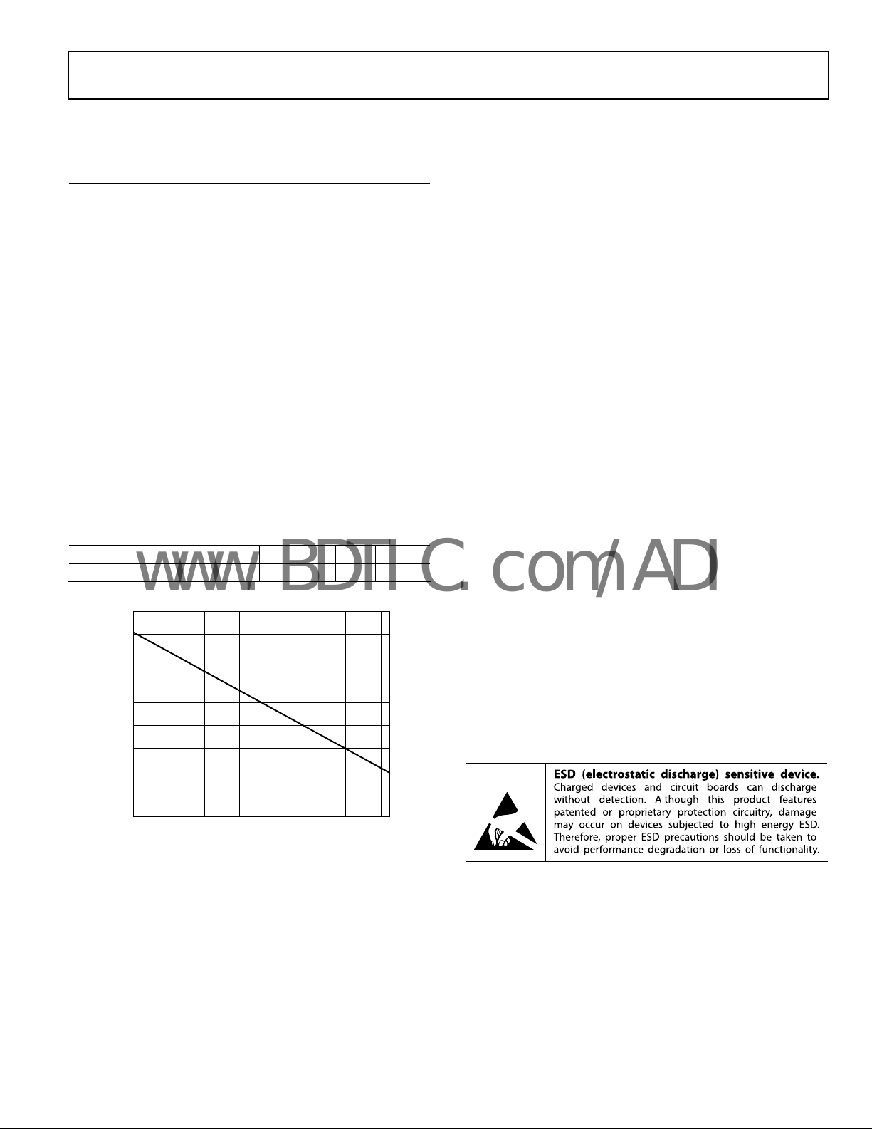
Power Dissipation See Figure 2
Storage Temperature Range –65°C to +125°C
Operating Temperature Range –40°C to +105°C
Lead Temperature Range (Soldering 10 sec) 300°C
Junction Temperature 150°C
Stresses above those listed under Absolute Maximum Ratings
may cause permanent damage to the device. This is a stress
rating only; functional operation of the device at these or any
other conditions above those indicated in the operational
section of this specification is not implied. Exposure to absolute
maximum rating conditions for extended periods may affect
device reliability.
THERMAL RESISTANCE
θJA is specified for the worst-case conditions, that is, θJA is
specified for a device soldered in the circuit board with its
exposed paddle soldered to a pad on the PCB surface, which is
thermally connected to a copper plane.
Table 4. Thermal Resistance
Package Type θJA θ
5 mm × 5 mm, 32-Lead LFCSP 47 8.5 °C/W
4.5
4.0
3.5
3.0
2.5
2.0
1.5
1.0
MAXIMUM POWER DISSIPATION (W)
0.5
0
–40 –20 0 20 40 60 80 100
AMBIENT TEMPERATURE (°C)
Figure 2. Maximum Power Dissipation vs. Temperature for a 4-Layer Board
Unit
JC
06307-002
Maximum Power Dissipation
The maximum safe power dissipation in the AD8145 package is
limited by the associated rise in junction temperature (T
) on
J
the die. At approximately 150°C, which is the glass transition
temperature, the plastic changes its properties. Even temporarily
exceeding this temperature limit can change the stresses that the
package exerts on the die, permanently shifting the parametric
performance of the AD8145. Exceeding a junction temperature
of 150°C for an extended period of time can result in changes in
the silicon devices, potentially causing failure.
The power dissipated in the package (P
) is the sum of the
D
quiescent power dissipation and the power dissipated in the
package due to the load drive for all outputs. The quiescent
power is the voltage between the supply pins (V
quiescent current (I
). The power dissipated due to the load
S
) times the
S
drive depends upon the particular application. For each output,
the power due to load drive is calculated by multiplying the load
current by the associated voltage drop across the device. The
power dissipated due to all of the loads is equal to the sum of
the power dissipation due to each individual load. RMS voltages
and currents must be used in these calculations.
Airflow increases heat dissipation, effectively reducing θ
. Also,
JA
more metal directly in contact with the package leads from
metal traces, through-holes, ground, and power planes reduces
the θ
. The exposed paddle on the underside of the package
JA
must be soldered to a pad on the PCB surface, which is
thermally connected to a copper plane to achieve the specified θ
.
JA
Figure 2 shows the maximum safe power dissipation in the
ackage vs. the ambient temperature for the 32-lead LFCSP
p
(47°C/W) on a JEDEC standard 4-layer board with the
underside paddle soldered to a pad, which is thermally
connected to a PCB plane.
ESD CAUTION
Rev. 0 | Page 7 of 24
Page 8
AD8145
G
www.BDTIC.com/ADI
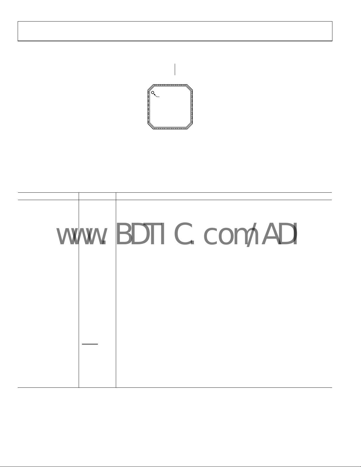
PIN CONFIGURATION AND FUNCTION DESCRIPTION
_B
S–
V
DIS/PD
REF_B
GAIN
IN+_B
IN–_B
GND
30
31
32
GND
26
27
28
29
25
15
14
UT
COMPB_OUT
COMPA_O
24 GND
23 OUT_B
22 OUT_G
21 OUT_R
20 V
19 COMPB_IN+
18 COMPB_IN–
17 GND
16
GND
S+
06307-003
1GND
PIN 1
2REF_G
INDICATO R
3
AIN_G
4IN+_G
AD8145
5IN–_G
TOP VIEW
6REF_R
(Not to Scale)
7GAIN_R
8GND
9
12
13
11
10
ND
G
IN–_R
IN+_R
COMPA_IN–
NOTES
1. EXPOSE D PAD ON UNDERSIDE O F DEVICE
MUST BE CONNECT ED TO GRO UND.
COMPA_IN+
Figure 3. 32-Lead LFCSP Pin Configuration
Table 5. 32-Lead LFCSP Pin Function Descriptions
Pin No. Mnemonic Description
1, 8, 9,16, 17, 24, 25, 32 GND Signal Ground and Thermal Plane Connection. (See the Absolute Maximum Ratings section.)
2 REF_G Reference Input, Green Channel.
3 GAIN_G Gain Connection, Green Channel.
4 IN+_G Noninverting Input, Green Channel.
5 IN−_G Inverting Input, Green Channel.
6 REF_R Reference Input, Red Channel.
7 GAIN_R Gain Connection, Red Channel.
10 IN+_R Noninverting Input, Red Channel.
11 IN−_R Inverting Input, Red Channel.
12 COMPA_IN+ Positive Input, Comparator A.
13 COMPA_IN- Negative Input, Comparator A.
14 COMPA_OUT Output, Comparator A.
15 COMPB_OUT Output, Comparator B.
18 COMPB_IN- Negative Input, Comparator B.
19 COMPB_IN+ Positive Input, Comparator B.
20 VS+ Positive Power Supply.
21 OUT_R Output, Red Channel.
22 OUT_G Output, Green Channel.
23 OUT_B Output, Blue Channel.
26 VS− Negative Power Supply.
27
DIS/PD
Disable/Power Down.
28 REF_B Reference Input, Blue Channel.
29 GAIN_B Gain Connection, Blue Channel.
30 IN+_B Noninverting Input, Blue Channel.
31 IN−_B Inverting Input, Blue Channel.
Exposed Underside Pad GND Signal Ground and Thermal Plane Connection.
Rev. 0 | Page 8 of 24
Page 9

AD8145
www.BDTIC.com/ADI
TYPICAL PERFORMANCE CHARACTERISTICS
Unless otherwise noted, G = 1, RL = 150 Ω, CL = 2 pF, REF = midsupply, VS = ±5 V, TA = 25°C. Refer to the circuit in Figure 35.
3
2
1
0
–1
–2
GAIN (dB)
–3
–4
–5
–6
V
= 0.2V p-p
OUT
–7
1 1000
10 100
FREQUE NCY (MHz )
+5V
±5V
06307-004
Figure 4. Small Signal Frequency Response at Various Power Supplies, G = 1
3
2
1
0
–1
–2
GAIN (dB)
–3
–4
–5
–6
V
= 2V p-p
OUT
–7
1 1000
10 100
FREQUE NCY (MHz )
+5V
±5V
06307-007
Figure 7. Large Signal Frequency Response at Various Power Supplies, G = 1
9
8
7
6
5
4
GAIN (dB)
3
2
1
0
V
= 0.2V p-p
OUT
–1
1 1000
10 100
FREQUE NCY (MHz )
+5V
±5V
06307-005
Figure 5. Small Signal Frequency Response at Various Power Supplies, G = 2
3
2
1
0
–1
–2
GAIN (dB)
–3
–4
–5
–6
–7
1 1000
G = 2, C
G = 2, C
G = 1, C
G = 1, C
V
OUT
= 10 + 2pF, R
L
= 0 + 2pF, R
L
= 10 + 2pF, R
L
= 0 + 2pF, R
L
= 0.2V p-p
= 20Ω
SNUB
= 0Ω
SNUB
= 20Ω
SNUB
= 0Ω
SNUB
10 100
FREQUE NCY (MHz )
06307-006
Figure 6. Small Signal Frequency Response at Various Gains
and
10 pF Capacitive Load Buffered by 20 Ω Resistor
9
8
7
6
5
4
GAIN (dB)
3
2
1
0
V
= 2V p-p
OUT
–1
1 1000
10 100
FREQUE NCY (MHz )
+5V
±5V
06307-008
Figure 8. Large Signal Frequency Response at Various Power Supplies, G = 2
3
2
1
0
–1
G = 2, CL = 10 + 2pF, R
= 0 + 2pF, R
G = 2, C
–2
GAIN (dB)
–3
–4
–5
–6
–7
L
= 10 + 2pF, R
G = 1, C
L
= 0 + 2pF, R
G = 1, C
L
V
= 2V p-p
OUT
1 1000
= 20Ω
SNUB
= 0Ω
SNUB
= 20Ω
SNUB
= 0Ω
SNUB
10 100
FREQUE NCY (MHz )
06307-009
Figure 9. Large Signal Frequency Response at Various Gains
and
10 pF Capacitive Load Buffered by 20 Ω Resistor
Rev. 0 | Page 9 of 24
Page 10

AD8145
www.BDTIC.com/ADI
3
2
1
0
–1
–2
GAIN (dB)
–3
–4
–5
–6
V
= 0.2V p-p
OUT
–7
1 1000
10 100
FREQUE NCY (MHz )
G = 2
Figure 10. Small Signal Frequency Response at Various Gains
0.5
0.4
0.3
0.2
0.1
0
GAIN (dB)
–0.1
–0.2
–0.3
–0.4
V
= 2V p-p
OUT
–0.5
1 1000
G = 1, VS = +5V
G = 1, VS = ±5V
G = 2, VS = +5V
= ±5V
G = 2, V
S
10 100
FREQUE NCY (MHz )
Figure 11. 0.1 dB Flatness for Various Power Supplies and Gains
G = 1
3
2
1
0
–1
–2
GAIN (dB)
–3
–4
–5
–6
V
= 2V p-p
OUT
–7
1 1000
06307-010
10 100
FREQUE NCY (MHz )
G = 2
G = 1
06307-013
Figure 13. Large Signal Frequency Response at Various Gains
1000
100
INPUT VOLTAGE NOISE (nV/ Hz)
10
0.01 100000
0.1 1 10 100 1000 10000
06307-011
FREQUENCY (kHz)
06307-046
Figure 14. Input Referred Voltage Noise vs. Frequency
110
100
90
80
70
60
50
40
30
COMMON-MO DE REJECTI ON (dB)
20
10
0.1 1000
1 10 100
FREQUE NCY (MHz )
Figure 12. Common-Mode Rejection vs. Freque
VS = +5V
VS = ±5V
ncy at Various Supplies
06307-012
4
RL = OPEN CIRCUIT
G = 1
3
V
= ±5V
S
2
1
0
–1
OUTPUT VOLTAGE (V)
–2
–3
–4
–5 5
–4–3–2–101234
DIFFERENTIAL INPUT VOLTAGE (V)
Figure 15. Differential Input Operating Range
Rev. 0 | Page 10 of 24
06307-047
Page 11

AD8145
www.BDTIC.com/ADI
150
1.5
100
50
0
VOLTAGE (mV)
–50
–100
V
= 0.2V p-p
OUT
–150
0 100
10 20 30 40 50 60 70 80 90
BLACK = +5V
GRAY = ±5V
TIME (ns)
06307-016
Figure 16. Small Signal Transient Response at Various Power Supplies, G = 1
150
100
50
0
VOLTAGE (mV)
–50
BLACK = +5V
GRAY = ±5V
1.0
0.5
0
VOLTAGE (V)
–0.5
–1.0
V
= 2V p-p
OUT
–1.5
0 100
10 20 30 40 50 60 70 80 90
BLACK = +5V
GRAY = ±5V
TIME (ns)
06307-019
Figure 19. Large Signal Transient Response at Various Power Supplies, G = 1
1.5
VOLTAGE (V)
1.0
0.5
0
–0.5
BLACK = +5V
GRAY = ±5V
–100
V
= 0.2V p-p
OUT
–150
0 100
10 20 30 40 50 60 70 80 90
TIME (ns)
06307-017
Figure 17. Small Signal Transient Response at Various Power Supplies, G = 2
150
100
50
0
VOLTAGE (mV)
–50
–100
G = 2, CL = 0 + 2pF, R
G = 2, C
= 10 + 2pF, R
–150
0 100
L
10 20 30 40 50 60 70 80 90
G = 1, CL = 0 + 2pF, R
G = 1, C
= 10 + 2pF, R
L
V
= 0.2V p-p
OUT
= 0Ω
SNUB
= 20Ω
SNUB
TIME (ns)
SNUB
SNUB
= 0Ω
= 20Ω
06307-018
Figure 18. Small Signal Transient Response at Various Gains
and
10 pF Capacitive Load Buffered by 20 Ω Resistor
–1.0
V
= 2V p-p
OUT
–1.5
0 100
10 20 30 40 50 60 70 80 90
TIME (ns)
06307-020
Figure 20. Large Signal Transient Response at Various Power Supplies, G = 2
1.5
1.0
0.5
0
VOLTAGE (V)
–0.5
–1.0
G = 2, CL = 0 + 2pF, R
G = 2, C
= 10 + 2pF, R
–1.5
0 100
L
10 20 30 40 50 60 70 80 90
G = 1, CL = 0 + 2pF, R
G = 1, C
= 10 + 2pF, R
L
V
= 2V p-p
OUT
= 0Ω
SNUB
= 20Ω
SNUB
TIME (ns)
SNUB
SNUB
= 0Ω
= 20Ω
06307-021
Figure 21. Large Signal Transient Response at Various Gains
and
10 pF Capacitive Load Buffered by 20 Ω Resistor
Rev. 0 | Page 11 of 24
Page 12

AD8145
–
–
–
–
www.BDTIC.com/ADI
2.0
1.6
INPUT
1.2
0.8
0.4
0
–0.4
VOLTAGE (V)
–0.8
–1.2
–1.6
–2.0
05
OUTPUT
ERROR
5 1015202530354045
TIME (ns)
0.5
0.4
0.3
0.2
0.1
0
ERROR (%)
–0.1
–0.2
–0.3
–0.4
–0.5
0
06307-048
4500
4000
3500
3000
2500
2000
1500
SLEW RATE (V/µs)
1000
500
0
05.0
Figure 22. Settling Time
50
–55
–60
–65
–70
DISTORTION (dBc)
–75
V
= 2V p-p
OUT
–80
0.1 100
VS = ±5V
VS = +5V
110
FREQUENCY (MHz)
06307-023
50
–60
–70
–80
–90
DISTORTION (dBc)
–100
–110
V
–120
0.1 100
POSITIVE
EW RATE
SL
NEGATIVE
EW RATE
SL
0.5 1.0 1.5 2.0 2.5 3.0 3.5 4.0 4.5
OUTPUT VOLTAGE (V p-p)
Figure 25. Slew Rate vs. Input Voltage Swing
VS = +5V
VS = ±5V
= 2V p-p
OUT
110
FREQUENCY (MHz)
06307-049
06307-026
Figure 23. Second Harmonic Distortion vs. Frequency and Power Supplies,
= 2 V p-p, G = 1
V
O
50
V
= 2V p-p
OUT
–55
–60
–65
–70
DISTORTION (dBc)
–75
–80
0.1 100
VS = ±5V
VS = +5V
110
FREQUENCY (MHz)
06307-024
Figure 24. Second Harmonic Distortion vs. Frequency and Power Supplies,
V
= 2 V p-p, G = 2
O
Rev. 0 | Page 12 of 24
Figure 26. Third Harmonic Distortion vs. Frequency and Power Supplies,
V
= 2 V p-p, G = 1
O
50
–60
–70
–80
–90
DISTORTION (dBc)
–100
–110
V
= 2V p-p
OUT
–120
0.1 100
VS = +5V
VS = ±5V
110
FREQUENCY (MHz)
06307-027
Figure 27. Third Harmonic Distortion vs. Frequency and Power Supplies,
V
= 2 V p-p, G = 2
O
Page 13

AD8145
www.BDTIC.com/ADI
65
RL = OPEN CIRCUIT
60
55
50
45
40
35
30
SUPPLY CURRENT (mA)
25
20
15
–60 120
IEE (±5V)
–40 –20 0 20 40 60 80 100
ICC (±5V)
IEE (±2.5V)
ICC (±2.5V)
TEMPERATURE (° C)
Figure 28. Power Supply Current vs. Temperature
06307-050
5
4
3
2
1
0
–1
VOLTAGE (V)
–2
–3
–4
G = 2
–5
05
50 100 150 200 250 300 350 400 450
+5V 2 × V
±5V OUTPUT
±5V 2 × V
TIME (ns)
Figure 31. Output Ove
+5V OUTPUT
IN
IN
rdrive Recovery
00
06307-030
10
0
–10
–20
–30
–40
PSRR (dB)
–50
–60
–70
–80
–90
0.01 1000
BLACK = +5V
GRAY = ±5V
0.1 1 10 100
FREQUENCY (MHz)
Figure 29. Positive Power Supply Rejection Ratio vs. Frequency
3.5
3.0
2.5
2.0
(V)
OUT
V
1.5
10
0
–10
–20
–30
–40
PSRR (dB)
–50
–60
–70
–80
–90
0.01 1000
06307-029
Figure 32. Negative Power Supply Re
BLACK = ±2.5V
GRAY = ±5V
0.1 1 10 100
FREQUE NCY (MHz )
jection Ratio vs. Frequency
06307-032
1.0
0.5
0
–15 15
–10 –5 0 5 10
V
(mV)
IN
06307-051
Figure 30. Comparator Hysteresis
Rev. 0 | Page 13 of 24
Page 14

AD8145
www.BDTIC.com/ADI
THEORY OF OPERATION
The AD8145 amplifiers use an architecture called active feedback,
which differs from that of conventional op amps. The most
obvious differentiating feature is the presence of two separate
pairs of differential inputs compared to a conventional op amp’s
single pair. Typically, for the active-feedback architecture, one of
these input pairs is driven by a differential input signal, while
the other is used for the feedback. This active stage in the feedback
path is where the term active feedback is derived. The AD8145
has an internal feedback resistor from each amplifier output to
the negative input of its feedback input stage. This limits the
possible closed-loop gain configurations for the AD8145.
The active feedback architecture offers several advantages over a
c
onventional op amp in several types of applications. Among
these are excellent common-mode rejection, wide input commonmode range, and a pair of inputs that are high impedance and
completely balanced in a typical application. In addition, while
an external feedback network establishes the gain response as in
a conventional op amp, its separate path makes it entirely
independent of the signal input. This eliminates any interaction
between the feedback and input circuits, which traditionally
causes problems with CMRR in conventional differential-input
op amp circuits.
Another advantage of active feedback is the ability to change the
p
olarity of the gain merely by switching the differential inputs.
A high input impedance inverting amplifier can therefore be
made. Besides high input impedance, a unity-gain inverter with
the AD8145 has noise gain of unity, producing lower output
noise and higher bandwidth than op amps that have noise gain
equal to 2 for a unity-gain inverter.
The two differential input stages of the AD8145 are each
t
ransconductance stages that are well matched. These stages
convert the respective differential input voltages to internal
currents. The currents are then summed and converted to a
voltage, which is buffered to drive the output. The compensation
capacitor is included in the summing circuit. When the
feedback path is closed around the part, the output drives
the feedback input to that voltage which causes the internal
currents to sum to zero. This occurs when the two differential
inputs are equal and opposite; that is, their algebraic sum is zero.
In a closed-loop application, a conventional op amp has its
ferential input voltage driven to near zero under non-
dif
transient conditions. The AD8145 generally has differential
input voltages at each of its input pairs, even under equilibrium
conditions. As a practical consideration, it is necessary to
internally limit the differential input voltage with a clamp
circuit. Thus, the input dynamic ranges are limited to about
2.5 V for the AD8145 (see the
det
ail). For this and other reasons, it is not recommended to
reverse the input and feedback stages of the AD8145, even
though some apparently normal functionality may be observed
under some conditions.
Specifications section for more
Rev. 0 | Page 14 of 24
Page 15

AD8145
V
T
V
V
V
www.BDTIC.com/ADI
APPLICATIONS
OVERVIEW
The AD8145 contains three independent active feedback amplifiers
that can be effectively applied as differential line receivers for
red-green-blue (RGB) signals or component video signals, such
as YPbPr, transmitted over unshielded twisted pair (UTP) cable.
The AD8145 also contains two general-purpose comparators
with hysteresis that can be used to receive digital signals or to
extract video synchronization pulses from received commonmode signals that contain encoded synchronization signals.
The comparators, which receive power from the positiv
supply, are referenced to GND and require greater than 4.5 V
on the positive supply for proper operation. If the comparators
are not used, then a split ±2.5 V can be used with the amplifiers
operating normally.
The AD8145 includes a power-down feature that can be
serted to reduce the supply current when a particular device
as
is not in use.
BASIC CLOSED-LOOP GAIN CONFIGURATIONS
Each amplifier in the AD8145 comprises two transconductance
amplifiers—one for the input signal and one for negative feedback.
It is important to note that the closed-loop gain of the amplifier
used in the signal path is defined as the single-ended output
voltage of the amplifier divided by its differential input voltage.
Therefore, each amplifier in the AD8145 provides differentialto-single-ended gain. Additionally, the amplifier used for
feedback has two high impedance inputs—the feedback input,
where the negative feedback is applied, and the REF input,
which can be used as an independent single-ended input to
apply a dc offset to the output signal.
The AD8145 contains on-chip feedback networks between each
a
mplifier output and its respective feedback input. Closed-loop
gain of an amplifier is set to 1 by connecting the amplifier output
directly to its respective GAIN pin. Doing this places the onchip resistors and capacitor in parallel across the amplifier
output and feedback pin. The small feedback capacitor
mitigates the effects of summing-node capacitance, which is
most problematic in the unity gain case. Closed-loop gain of an
amplifier is set to 2 by connecting the respective GAIN pin to a
reference voltage, often directly to ground. In
nd C = 2 pF.
a
Some basic gain configurations implemented with an AD8145
a
mplifier are shown in Figure 33 through Figure 36.
Figure 1, R = 350
e
+5
0.01µF
V
IN
OUT
REF
REF
–5V
Figure 33. Basic Gain = 1 Circuit: V
R
R
C
0.01µF
= VIN + V
OUT
GAIN
V
OU
06307-034
REF
The gain equation for the circuit in Figure 33 is
V
OUT
= VIN + V
(1)
REF
In this configuration, the voltage applied to the REF pin appears
a
t the output with a gain of 1.
Figure 34 illustrates one way to operate an AD8145 amplifier
wi
th a gain of 2.
+5
0.01µF
V
IN
REF
REF
GAIN
Figure 34. Basic Gain = 2 Circuit: V
C
–5V
RR
0.01µF
= 2(VIN + V
OUT
V
OUT
06307-035
)
REF
The gain equation for the circuit in Figure 34 is
= 2(VIN + V
V
OUT
) (2)
REF
Rev. 0 | Page 15 of 24
Page 16

AD8145
V
V
V
T
Ω
V
T
Ω
www.BDTIC.com/ADI
To achieve unity gain from V
divide V
divider resistors, R
by the same factor used in the feedback loop; the
REF
, need not be the same values used in the
D
internal feedback loop. Figure 35 illustrates this approach.
R
D
R
GAIN
D
C
V
REF
Figure 35. Basic Gain Circuit: V
The gain equation for the circuit in Figure 35 is
V
= 2VIN + V
OUT
REF
Another configuration that provides the same gain equation as
uation 3 is shown in Figure 36. In this configuration, it is
Eq
im
portant to keep the source resistance of V
than 350 to avoid gain errors.
V
IN
REF
C
GAIN
V
REF
Figure 36. Basic Gain Circuit: V
For stability reasons, the inductance of the trace connected to
the REF pin must be kept to less than 10 nH. The typical
inductance of 50 Ω traces on the outer layers of the FR-4 boards
is 7 nH/in, and on the inner layers, it is typically 9 nH/in. Vias
must be accounted for as well. The inductance of a typical via in
a 0.062 inch board is on the order of 1.5 nH. If longer traces are
required, a 200 Ω resistor should be placed in series with the
trace to reduce the Q-factor of the inductance.
In many dual-supply applications, V
connected to ground right at the device.
to V
REF
in this configuration,
OUT
TERMINATING THE INPUT
One of the key benefits of the active feedback architecture is the
separation that exists between the differential input signal and
the feedback network. Because of this separation, the differential
+5
0.01µF
V
IN
REF
V
OUT
input maintains its high CMRR and provides high differential
and common-mode input impedances, making line termination
a simple task.
Most applications that use the AD8145 involve transmitting
roadband video signals over 100 Ω UTP cable and use
b
dc-coupled terminations. The two most common types of
dc-coupled terminations are differential and common-mode.
Differential termination of 100 Ω UTP is implemented by
RR
0.01µF
–5V
= 2VIN + V
OUT
REF
06307-036
(3)
much smaller
REF
+5
0.01µF
V
OUT
simply connecting a 100 Ω resistor across the amplifier input,
as shown in
100
Figure 37.
+5
V
UTP
100Ω
Figure 37. Differential-Mode Termination with G = 1
IN
REF
R
R
C
–5V
0.01µF
0.01µF
OUT
GAIN
V
OU
06307-038
Some applications require common-mode terminations for
common-mode currents generated at the transmitter. In these
cases, the 100 Ω termination resistor is split into two 50 Ω
RR
resistors. The required common-mode termination voltage is
applied at the tap between the two resistors. In many of these
–5V
OUT
can be directly
REF
0.01µF
= 2VIN + V
REF
06307-037
applications, the common-mode tap is connected to ground
(V
(CM) = 0). This scheme is illustrated in Figure 38.
TERM
+5
0.01µF
(CM)
50Ω
50Ω
V
IN
REF
OUT
V
OU
R
R
C
GAIN
100
UTP
V
TERM
Figure 38. Common-Mode Termination with G = 1
Rev. 0 | Page 16 of 24
–5V
0.01µF
06307-039
Page 17

AD8145
V
V
www.BDTIC.com/ADI
INPUT CLAMPING
The differential input that is assigned to receive the input signal
includes clamping diodes that limit the differential input swing
to approximately 5.5 V p-p at 25°C. Because of this, the input
and feedback stages should never be interchanged.
The supply current drawn by the AD8145 has a strong
dep
endence on input signal magnitude because the input
transconductance stages operate with differential input signals
that can be up to a few volts peak-to-peak. This behavior is
distinctly different from that of traditional op amps, where the
differential input signal is driven to essentially 0 V by negative
feedback.
For most applications, including receiving RGB video signals,
he input signal magnitudes encountered are well within the
t
safe operating limits of the AD8145 over its full power supply
and operating temperature ranges. In some extreme applications
where large differential and/or common-mode voltages are
encountered, external clamping may be necessary. Another
application in which external common-mode clamping is
sometimes required is when an unpowered AD8145 receives a
signal from an active driver. In this case, external diodes are
required when the current drawn by the internal ESD diodes
cannot be kept to less than 5 mA.
Figure 39 shows a general approach to external differential-
ode clamping.
m
REF
+5
–5V
R
R
C
0.01µF
0.01µF
OUT
GAIN
V
OUT
06307-040
POSITI VE CLAMP NEGATIVE CLAMP
+
R
S
V
IN
R
T
R
–
S
Figure 39. Differential-Mode Clamping with G = 1
The positive and negative clamps are nonlinear devices that
exhibit very low impedance when the voltage across them
reaches a critical threshold (clamping voltage), thereby limiting
the voltage across the AD8145 input. The positive clamp has a
positive threshold, and the negative clamp has a negative
threshold.
A diode is a simple example of such a clamp. Schottky diodes
g
enerally have lower clamping voltages than typical signal
diodes. The clamping voltage should be larger than the largest
expected signal amplitude, with enough margin to ensure that
the received signal passes without being distorted.
A simple way to implement a clamp is to use a number of
dio
des in series. The resultant clamping voltage is then the sum
of the clamping voltages of individual diodes.
A 1N4448 diode has a forward voltage of approximately 0.70 V
o 0.75 V at typical current levels that are seen when it is being
t
used as a clamp, and 2 pF maximum capacitance at 0 V bias.
(The capacitance of a diode decreases as its reverse bias voltage
is increased.) The series connection of two 1N4448 diodes,
therefore, has a clamping voltage of 1.4 V to 1.5 V.
hows how to limit the differential input voltage applied to an
s
Figure 40
AD8145 amplifier to ±1.4 V to ±1.5 V (2.8 V p-p to 3.0 V p-p).
Note that the capacitance of the two series diodes is half that of
one diode. Different numbers of series diodes can be used to
obtain different clamping voltages.
is the differential termination resistor, and the series
R
T
resistances, R
, limit the current into the diodes. The series
S
resistors should be highly matched in value to preserve high
frequency CMRR.
+5
POSITIVE CLAMP NEGATIVE CLAMP
R
R
C
0.01µF
0.01µF
OUT
GAIN
V
OUT
06307-041
+
R
S
V
R
IN
T
R
–
S
REF
–5V
Figure 40. Using Two 1N4448 Diodes in Series as a Clamp
There are many other nonlinear devices that can be used as
clamps. The best choice for a particular application depends
upon the desired clamping voltage, response time, parasitic
capacitance, and other factors.
When using external differential-mode clamping, it is
im
portant to ensure that the series resistors (R
), the sum of
S
the parasitic capacitance of the clamping devices, and the input
capacitance of the AD8145 are small enough to preserve the
desired signal bandwidth.
Rev. 0 | Page 17 of 24
Page 18

AD8145
V
V
–
www.BDTIC.com/ADI
Figure 41 shows a specific example of external common-mode
clamping.
+
2
REF
+5V
–5V
R
R
C
0.01µF
0.01µF
OUT
GAIN
V
OUT
06307-042
+
IN
R
S
HBAT-540C
R
T
R
S
HBAT-540C
Figure 41. External Common-Mode Clamping
3
1
V–
V+
2
3
1
V–
The series resistances, RS, limit the current in each leg,
and the Schottky diodes limit the voltages on each input to
approximately 0.3 V to 0.4 V over the positive power supply,
V+, and to 0.3 V to 0.4 V below the negative power supply, V−.
The maximum value of R
is determined by the required signal
S
bandwidth, the line impedance, and the effective differential
capacitance due to the AD8145 inputs and the diodes.
As with the differential clamp, the series resistors should be
hly matched in value to preserve high frequency CMRR.
hig
PRINTED CIRCUIT BOARD LAYOUT CONSIDERATIONS
The two most important issues with regard to printed circuit
board (PCB) layout are minimizing parasitic signal trace
reactances in the feedback network and providing sufficient
thermal relief.
Excessive parasitic reactances in the feedback network cause
excessi
ve peaking in the frequency response of the amplifier
and excessive overshoot in its step response due to a reduction
in phase margin. Oscillation occurs when these parasitic
reactances are increased to a critical point where the phase
margin is reduced to zero. Minimizing these reactances is
important to obtain optimal performance from the AD8145.
General high speed layout practices should be adhered to when
applying the AD8145. Controlled impedance transmission lines
are required for incoming and outgoing signals, referenced to a
ground plane.
Typically, the input signals are received over 100 Ω differential
tra
nsmission lines. A 100 Ω differential transmission line is
readily realized on the printed circuit board using two wellmatched, closely-spaced, 50 Ω single-ended traces that are
coupled through the ground plane. The traces that carry the
single-ended output signals are most often 75 Ω for video
signals. Output signal connections should include series
termination resistors that are matched to the impedance of the
line they are driving. When driving high impedance loads over
very short traces, impedance matching is not required. In these
cases, small series resistors should be used to buffer the
capacitance presented by the load.
Broadband power supply decoupling networks should be placed
close as possible to the supply pins. Small surface-mount
as
ceramic capacitors are recommended for these networks, and
tantalum capacitors are recommended for bulk supply
decoupling.
Minimizing Parasitic Feedback Reactances
Parasitic trace capacitance and inductance are both reduced in
the unity-gain configuration when the feedback trace that
connects the OUT pin to the GAIN pin is reduced in length.
Removing the copper from all planes below the trace reduces
trace capacitance, but increases trace inductance, since the loop
area formed by the trace and ground plane is increased. A
reasonable compromise that works well is to void all copper
directly under the feedback trace and component pads with
margins on each side approximately equal to one trace width.
Combining this technique with minimizing trace length is
effective in keeping parasitic trace reactance in the unity-gain
feedback loop to a minimum.
Maximizing Heat Removal
A 5 × 5 array of thermal vias works well to connect the exposed
paddle to internal ground planes. The vias should be placed
inside the PCB pad that is soldered to the exposed paddle, and
should connect to all ground planes.
The AD8145 includes ground connections on its corner pins.
Th
ese pins can be used to provide additional heat removal from
the AD8145 by connecting them between the PCB pad that is
soldered to the exposed paddle and a ground plane on the
component side of the board. This layout technique lowers the
overall package thermal resistance. Use of this technique is not
required, but it does result in a lower junction temperature.
Designs must often conform to design for manufacturing
(DFM) rules that stipulate how to lay out PCBs in such a way as
to facilitate the manufacturing process. Some of these rules
require thermal relief on pads that connect to planes, and the
rules may limit the extent to which this technique can be used.
Rev. 0 | Page 18 of 24
Page 19

AD8145
V
V
V
www.BDTIC.com/ADI
DRIVING A CAPACITIVE LOAD
The AD8145 typically drives either high impedance loads over
short PCB traces, such as crosspoint switch inputs, or doubly
terminated coaxial cables. A gain of 1 is commonly used in the
high impedance case since the 6 dB transmission line termination
loss is not incurred. A gain of 2 is required when driving cables
to compensate for the 6 dB termination loss.
In all cases, the output must drive the parasitic capacitance
f the feedback loop, conservatively estimated to be 1 pF, in
o
addition to the capacitance presented by the actual load. When
driving a high impedance input, it is recommended that a small
series resistor be used to buffer the input capacitance of the
device being driven. Clearly, the resistor value must be small
enough to preserve the required bandwidth. In the ideal doubly
terminated cable case, the AD8145 output sees a purely resistive
load. In reality, there is some residual capacitance, and this is
buffered by the series termination resistor.
he high impedance case, and Figure 43 illustrates the cable-
t
dr
iving case.
Figure 42 illustrates
POWER-DOWN
The power-down feature is intended to be used to reduce power
consumption when a particular device is not in use, and does
not place the output in a high-Z state when asserted. The
power-down feature is asserted when the voltage applied to the
power-down pin drops to approximately 2 V below the positive
supply. The AD8145 is enabled by pulling the power-down pin
to the positive supply.
+5
0.01µF
V
IN
R
OUT
S
REF
REF
R
R
C
0.01µF
–5V
Figure 42. Buffering the Input Capacitance of a High-Z Load with G = 1
GAIN
C
IN
+5
0.01µF
V
IN
R
OUT
S
REF
V
REF
GAIN
C
RR
C
S
06307-043
R
L
0.01µF
–5V
Figure 43. Driving a Doubly Terminated Cable with G = 2
06307-044
Rev. 0 | Page 19 of 24
Page 20

AD8145
www.BDTIC.com/ADI
COMPARATORS
In addition to general-purpose applications, the two on-chip
comparators can be used to decode video sync pulses from the
received common-mode voltages, or to receive differential digital
information. Built-in hysteresis helps to eliminate false triggers
from noise.
The comparator outputs are designed to drive source-terminated
nsmission lines. The source termination technique uses a
tra
resistor in series with each comparator output such that the sum
of the comparator source resistance (≈ 20 ) and the series
resistor equals the transmission line characteristic impedance.
The load end of the transmission line is high impedance. When
the signal is launched into the source termination, its initial
value is one-half of its source value, since its amplitude is
divided by two by the voltage divider formed by the source
termination and the transmission line. At the load, the signal
experiences nearly 100% positive reflection due to the high
impedance load, and is restored to nearly its full value. This
technique is commonly used in PCB layouts that involve high
speed digital logic.
An internal linear voltage regulator derives power for the
co
mparators from the positive supply; therefore, the AD8145
must always have a minimum positive supply voltage of 4.5 V.
SYNC PULSE EXTRACTION USING COMPARATORS
The AD8145 is particularly useful in keyboard, video, mouse
(KVM) applications. KVM networks transmit and receive
computer video signals, which typically comprise red, green,
and blue (RGB) video signals and separate horizontal and
vertical sync signals. Because the sync signals are separate and
not embedded in the color signals, it is advantageous to
transmit them using a simple scheme that encodes them among
the three common-mode voltages of the RGB signals. The
AD8134 triple differential driver is a natural complement to the
AD8145 an
d performs the sync pulse encoding with the
necessary circuitry on-chip.
The AD8134 encoding equations are given in Equation 4,
uation 5,
Eq
and Equation 6.
K
CM
VGreen
CM
CM
[ ]
2
K
[ ]
K
[ ]
2
−=
+=
VRed
VBlue
(4)
HV
(5)
V22−=
(6)
HV
where:
Red V
, Green VCM, and Blue VCM are the transmitted common-
CM
mode voltages of the respective color signals.
n adjustable gain constant that is set by the AD8134.
K is a
H are the vertical and horizontal sync pulses, defined
V and
with a weight of −1 when the pulses are in their low states, and a
weight of +1 when they are in their high states.
The AD8134 data sheet contains further details regarding the
e
ncoding scheme. Figure 44 illustrates how the AD8145
mparators can be used to extract the horizontal and vertical
co
sync pulses that are encoded on the RGB common-mode
voltages by the AD8134.
50Ω
RECEIVED
RED VIDEO
RECEIVED
GREEN VIDEO
RECEIVED
BLUE VIDEO
Figure 44. Extracting Sync Signals from Received Common-Mode Signal
RED CMV
50Ω
50Ω
GREEN CMV
50Ω
50Ω
BLUE CMV
50Ω
Rev. 0 | Page 20 of 24
1kΩ
475Ω
1kΩ
47pF
47pF
R
S
HSYNC
R
S
VSYNC
06307-045
Page 21

AD8145
www.BDTIC.com/ADI
OUTLINE DIMENSIONS
0.60 MAX
25
24
EXPOSED
PAD
(BOTTOM VIEW)
17
16
32
1
8
9
3.50 REF
PIN 1
INDICATOR
3.45
3.30 SQ
3.15
0.25 MIN
PIN 1
INDICATOR
1.00
0.85
0.80
12° MAX
SEATING
PLANE
5.00
BSC SQ
TOP
VIEW
0.80 MAX
0.65 TYP
0.30
0.23
0.18
COMPLIANT TO JEDEC STANDARDS MO-220-VHHD-2
4.75
BSC SQ
0.20 REF
0.05 MAX
0.02 NOM
0.60 MAX
0.50
BSC
0.50
0.40
0.30
COPLANARITY
0.08
Figure 45. 32-Lead Lead Frame Chip Scale Package [LFCSP_VQ]
5
mm × 5 mm Body, Very Thin Quad
(CP-32-3)
Dimensions shown in millimeters
ORDERING GUIDE
Model Temperature Range Package Description Package Option
AD8145YCPZ-R2
AD8145YCPZ-RL
AD8145YCPZ-R7
1
Z = Pb-free part.
1
1
1
−40°C to +105°C 32-Lead Lead Frame Chip Scale Package [LFCSP_VQ] CP-32-3
−40°C to +105°C 32-Lead Lead Frame Chip Scale Package [LFCSP_VQ] CP-32-3
−40°C to +105°C 32-Lead Lead Frame Chip Scale Package [LFCSP_VQ] CP-32-3
Rev. 0 | Page 21 of 24
Page 22

AD8145
www.BDTIC.com/ADI
NOTES
Rev. 0 | Page 22 of 24
Page 23

AD8145
www.BDTIC.com/ADI
NOTES
Rev. 0 | Page 23 of 24
Page 24

AD8145
www.BDTIC.com/ADI
NOTES
©2006 Analog Devices, Inc. All rights reserved. Trademarks and
registered trademarks are the property of their respective owners.
D06307-0-10/06(0)
Rev. 0 | Page 24 of 24
 Loading...