

Page 1
Low Noise Rail-to-Rail
FEATURES
Fully differential
Low noise
2.25 nV/√Hz
2.1 pA/√Hz
Low harmonic distortion
98 dBc SFDR @ 1 MHz
85 dBc SFDR @ 5 MHz
72 dBc SFDR @ 20 MHz
High speed
410 MHz, 3 dB BW (G = 1)
800 V/µs slew rate
45 ns settling time to 0.01%
69 dB output balance @ 1 MHz
80 dB dc CMRR
Low offset: ±0.5 mV max
Low input offset current: 0.5 µA max
Differential input and output
Differential-to-differential or single-ended-to-differential
operation
Rail-to-rail output
Adjustable output common-mode voltage
Wide supply voltage range: 5 V to 12 V
Available in small SOIC package
GENERAL DESCRIPTION
The AD8139 is an ultralow noise, high performance differential
amplifier with rail-to-rail output. With its low noise, high SFDR,
and wide bandwidth, it is an ideal choice for driving ADCs with
resolutions to 18 bits. The AD8139 is easy to apply, and its internal common-mode feedback architecture allows its output
common-mode voltage to be controlled by the voltage applied
to one pin. The internal feedback loop also provides outstanding output balance as well as suppression of even-order
harmonic distortion products. Fully differential and singleended-to-differential gain configurations are easily realized by
the AD8139. Simple external feedback networks consisting of a
total of four resistors determine the amplifier’s closed-loop gain.
The AD8139 is manufactured on ADI’s proprietary second generation XFCB process, enabling it to achieve low levels of distortion with input voltage noise of only 1.85 nV/√Hz.
Differential ADC Driver
AD8139
APPLICATIONS
ADC drivers to 18 bits
Single-ended-to-differential converters
Differential filters
Level shifters
Differential PCB board drivers
Differential cable drivers
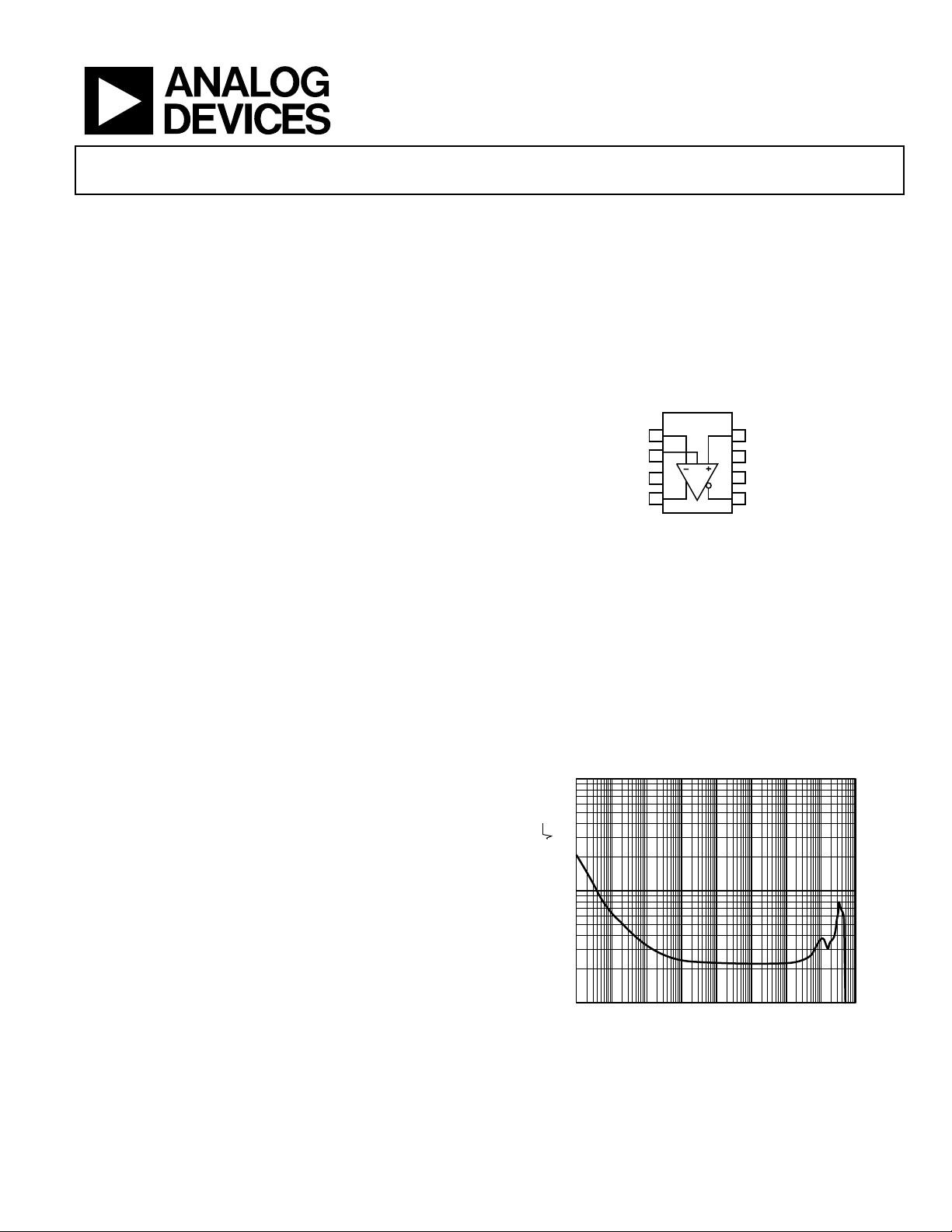
FUNCTIONAL BLOCK DIAGRAM
AD8139
–IN 1
2
V
OCM
V+ 3
+OUT 4
NC = NO CONNECT
Figure 1.
The AD8139 is available in an 8-lead SOIC package with an
exposed paddle (EP) on the underside of its body and a 3 mm ×
3 mm LFCSP. It is rated to operate over the temperature range
of −40°C to +125°C.
100
10
INPUT VOLTAGE NOISE (nV/ Hz)
1
10 100 1k 10k 100k 1M 10M 1G100M
Figure 2. Input Voltage Noise vs. Frequency
FREQUENCY (Hz)
+IN8
NC7
V–6
–OUT5
04679-0-001
04679-0-078
Rev. A
Information furnished by Analog Devices is believed to be accurate and reliable.
However, no responsibility is assumed by Analog Devices for its use, nor for any
infringements of patents or other rights of third parties that may result from its use.
Specifications subject to change without notice. No license is granted by implication
or otherwise under any patent or patent rights of Analog Devices. Trademarks and
registered trademarks are the property of their respective owners.
One Technology Way, P.O. Box 9106, Norwood, MA 02062-9106, U.S.A.
Tel: 781.329.4700
Fax: 781.326.8703 © 2004 Analog Devices, Inc. All rights reserved.
www.analog.com
Page 2

AD8139
TABLE OF CONTENTS
VS = ±5 V, V
= 0 V Specifications.............................................. 3
OCM
Typical Connection and Definition of Terms ........................ 18
VS = 5 V, V
= 2.5 V Specifications............................................. 5
OCM
Absolute Maximum Ratings............................................................ 7
Thermal Resistance ......................................................................7
ESD Caution.................................................................................. 7
Pin Configuration and Function Descriptions............................. 8
Typical Performance Characteristics............................................. 9
Theory of Operation ...................................................................... 18
REVISION HISTORY
8/04—Data Sheet Changed from a Rev. 0 to Rev. A.
Added 8-Lead LFCSP.........................................................Universal
Changes to General Description .................................................... 1
Changes to Figure 2.......................................................................... 1
Changes to V
Changes to V
= ±5 V, V
S
= 5 V, V
S
= 0 V Specifications......................... 3
OCM
= 2.5 V Specifications......................... 5
OCM
Changes to Table 4............................................................................ 7
Changes to Maximum Power Dissipation Section....................... 7
Changes to Figure 26 and Figure 29............................................. 12
Inserted Figure 39 and Figure 42.................................................. 14
Changes to Figure 45 to Figure 47................................................ 15
Inserted Figure 48........................................................................... 15
Changes to Figure 52 and Figure 53............................................. 16
Changes to Figure 55 and Figure 56............................................. 17
Changes to Table 6.......................................................................... 19
Changes to Voltage Gain Section.................................................. 19
Changes to Driving a Capacitive Load Section ..........................22
Changes to Ordering Guide.......................................................... 24
Updated Outline Dimensions....................................................... 24
Applications..................................................................................... 19
Estimating Noise, Gain, and Bandwidth with Matched
Feedback Networks
.................................................................... 19
Outline Dimensions....................................................................... 24
Ordering Guide .......................................................................... 24
5/04—Revision 0: Initial Version
Rev. A | Page 2 of 24
Page 3

AD8139
VS = ±5 V, V
@ 25°C, Diff. Gain = 1, R
= 0 V SPECIFICATIONS
OCM
= 1 kΩ, RF = RG = 200 Ω, unless otherwise noted. T
L, dm
MIN
to T
= −40°C to +125°C.
MAX
Table 1.
Parameter Conditions Min Typ Max Unit
DIFFERENTIAL INPUT PERFORMANCE
DYNAMIC PERFORMANCE
−3 dB Small Signal Bandwidth V
−3 dB Large Signal Bandwidth V
Bandwidth for 0.1 dB Flatness V
Slew Rate V
Settling Time to 0.01% V
Overdrive Recovery Time G = 2, V
= 0.1 V p-p 340 410 MHz
O, dm
= 2 V p-p 210 240 MHz
O, dm
= 0.1 V p-p 45 MHz
O, dm
= 2 V Step 800 V/µs
O, dm
= 2 V Step, CF = 2 pF 45 ns
O, dm
= 12 V p-p Triangle Wave 30 ns
IN, dm
NOISE/HARMONIC PERFORMANCE
SFDR V
V
V
Third-Order IMD V
= 2 V p-p, fC = 1 MHz 98 dB
O, dm
= 2V p-p, fC = 5 MHz 85 dB
O, dm
= 2 V p-p, fC = 20 MHz 72 dB
O, dm
= 2 V p-p, fC = 10.05 MHz ± 0.05 MHz −90 dBc
O, dm
Input Voltage Noise f = 100 KHz 2.25 nV/√Hz
Input Current Noise f = 100 KHz 2.1 pA/√Hz
DC PERFORMANCE
Input Offset Voltage VIP = VIN = V
Input Offset Voltage Drift T
Input Bias Current T
MIN
MIN
to T
to T
MAX
MAX
OCM
= 0 V
−500 ±150 +500 µV
1.25 µV/ºC
2.25 8.0 µA
Input Offset Current 0.12 0.5 µA
Open-Loop Gain 114 dB
INPUT CHARACTERISTICS
Input Common-Mode Voltage Range −4 +4 V
Input Resistance Differential 600 kΩ
Common Mode 1.5 MΩ
Input Capacitance Common Mode 1.2 pF
CMRR V
= ±1 V dc, RF = RG = 10 kΩ 80 84 dB
ICM
OUTPUT CHARACTERISTICS
Output Voltage Swing Each Single-Ended Output, RF = RG = 10 kΩ −VS + 0.20 +VS – 0.20 V
Each Single-Ended Output,
= Open Circuit, RF = RG = 10 kΩ
R
L, dm
+ 0.15 +VS – 0.15 V
−V
S
Output Current Each Single-Ended Output 100 mA
Output Balance Error f = 1 MHz −69 dB
V
to V
OCM
V
OCM
−3 dB Bandwidth V
Slew Rate V
PERFORMANCE
O, cm
DYNAMIC PERFORMANCE
= 0.1 V p-p 515 MHz
O, cm
= 2 V p-p 250 V/µs
O, cm
Gain 0.999 1.000 1.001 V/V
V
INPUT CHARACTERISTICS
OCM
Input Voltage Range −3.8 +3.8 V
Input Resistance 3.5 MΩ
Input Offset Voltage V
OS, cm
= V
O, cm
− V
; VIP = VIN = V
OCM
= 0 V −900 ±300 +900 µV
OCM
Input Voltage Noise f = 100 kHz 3.5 nV/√Hz
Input Bias Current 1.3 4.5 µA
CMRR V
/V
, V
OCM
O, dm
= ±1 V 74 88 dB
OCM
Rev. A | Page 3 of 24
Page 4

AD8139
Parameter Conditions Min Typ Max Unit
POWER SUPPLY
Operating Range 4.5 ±6 V
Quiescent Current 24.5 25.5 mA
+PSRR Change in +VS = ±1V 95 112 dB
−PSRR Change in −VS = ±1V 95 109 dB
OPERATING TEMPERATURE RANGE −40 +125 °C
Rev. A | Page 4 of 24
Page 5

AD8139
VS = 5 V, V
@ 25°C, Diff. Gain = 1, R
= 2.5 V SPECIFICATIONS
OCM
= 1 kΩ, RF = RG = 200 Ω, unless otherwise noted. T
L, dm
MIN
to T
= −40°C to +125°C.
MAX
Table 2.
Parameter Conditions Min Typ Max Unit
DIFFERENTIAL INPUT PERFORMANCE
DYNAMIC PERFORMANCE
−3 dB Small Signal Bandwidth V
−3 dB Large Signal Bandwidth V
Bandwidth for 0.1 dB Flatness V
Slew Rate V
Settling Time to 0.01% V
Overdrive Recovery Time G = 2, V
= 0.1 V p-p 330 385 MHz
O, dm
= 2 V p-p 135 165 MHz
O, dm
= 0.1 V p-p 34 MHz
O, dm
= 2 V Step 540 V/s
O, dm
= 2 V Step 55 ns
O, dm
= 7 V p-p Triangle Wave 35 ns
IN, dm
NOISE/HARMONIC PERFORMANCE
SFDR V
V
V
Third-Order IMD V
= 2 V p-p, fC = 1 MHz 99 dB
O, dm
= 2 V p-p, fC = 5 MHz, (RL = 800 Ω) 87 dB
O, dm
= 2 V p-p, fC = 20 MHz, (RL = 800 Ω) 75 dB
O, dm
= 2 V p-p, fC = 10.05 MHz ± 0.05 MHz −87 dBc
O, dm
Input Voltage Noise f = 100 kHz 2.25 nV/√Hz
Input Current Noise f = 100 kHz 2.1 pA/√Hz
DC PERFORMANCE
Input Offset Voltage VIP = VIN = V
Input Offset Voltage Drift T
Input Bias Current T
MIN
MIN
to T
to T
MAX
MAX
OCM
=0 V
−500 ±150 +500 µV
1.25 µV/ºC
2.2 7.5 A
Input Offset Current 0.13 0.5 µA
Open-Loop Gain 112 dB
INPUT CHARACTERISTICS
Input Common-Mode Voltage Range 1 4 V
Input Resistance Differential 600 KΩ
Common-Mode 1.5 MΩ
Input Capacitance Common-Mode 1.2 pF
CMRR ∆V
= ±1 V dc, RF = RG = 10 kΩ 75 79 dB
ICM
OUTPUT CHARACTERISTICS
Output Voltage Swing Each Single-Ended Output, RF = RG = 10 kΩ −VS + 0.15 +VS − 0.15 V
Each Single-Ended Output,
= Open Circuit, RF = RG = 10 kΩ
R
L, dm
+ 0.10 +VS − 0.10 V
−V
S
Output Current Each Single-Ended Output 80 mA
Output Balance Error f = 1 MHz −70 dB
V
to V
OCM
V
OCM
−3 dB Bandwidth V
Slew Rate V
PERFORMANCE
O, cm
DYNAMIC PERFORMANCE
= 0.1 V p-p 440 MHz
O, cm
= 2 V p-p 150 V/s
O, cm
Gain 0.999 1.000 1.001 V/V
V
INPUT CHARACTERISTICS
OCM
Input Voltage Range 1.0 3.8 V
Input Resistance 3.5 MΩ
Input Offset Voltage V
OS, cm
= V
O, cm
− V
; VIP = VIN = V
OCM
= 2.5 V −1.0 ±0.45 +1.0 mV
OCM
Input Voltage Noise f = 100 KHz 3.5 nV/√Hz
Input Bias Current 1.3 4.2 A
CMRR ∆V
/∆VO(dm), ∆V
OCM
= ±1 V 67 79 dB
OCM
Rev. A | Page 5 of 24
Page 6

AD8139
Parameter Conditions Min Typ Max Unit
POWER SUPPLY
Operating Range +4.5 ±6 V
Quiescent Current 21.5 22.5 mA
+PSRR Change in +VS = ±1 V 86 97 dB
−PSRR Change in −VS = ±1 V 92 105 dB
OPERATING TEMPERATURE RANGE −40 +125 °C
Rev. A | Page 6 of 24
Page 7
AD8139
ABSOLUTE MAXIMUM RATINGS
Table 3.
Parameter Rating
Supply Voltage 12 V
V
OCM
±V
S
Power Dissipation See Figure 3
Input Common-Mode Voltage ±V
S
Storage Temperature –65°C to +125°C
Operating Temperature Range –40°C to +125°C
Lead Temperature Range
300°C
(Soldering 10 sec)
Junction Temperature 150°C
Stresses above those listed under Absolute Maximum Ratings
may cause permanent damage to the device. This is a stress rating only; functional operation of the device at these or any
other conditions above those indicated in the operational section of this specification is not implied. Exposure to absolute
maximum rating conditions for extended periods may affect
device reliability.
THERMAL RESISTANCE
θJA is specified for the worst-case conditions, i.e., θJA is specified
for device soldered in circuit board for surface-mount packages.
Table 4. Thermal Resistance
Package Type θ
JA
SOIC-8 with EP/4-Layer 70 °C/W
LFCSP/4-Layer 70 °C/W
Maximum Power Dissipation
The maximum safe power dissipation in the AD8139 package is
limited by the associated rise in junction temperature (T
die. At approximately 150°C, which is the glass transition temperature, the plastic will change its properties. Even temporarily
exceeding this temperature limit may change the stresses that the
package exerts on the die, permanently shifting the parametric
Unit
) on the
J
The power dissipated in the package (P
quiescent power dissipation and the power dissipated in the
package due to the load drive for all outputs. The quiescent
power is the voltage between the supply pins (V
quiescent current (I
and common-mode currents flowing to the load, as well as
currents flowing through the external feedback networks and
the internal common-mode feedback loop. The internal resistor
tap used in the common-mode feedback loop places a 1 kΩ
differential load on the output. RMS output voltages should be
considered when dealing with ac signals.
Airflow reduces θ
the package leads from metal traces, through holes, ground, and
power planes will reduce the θ
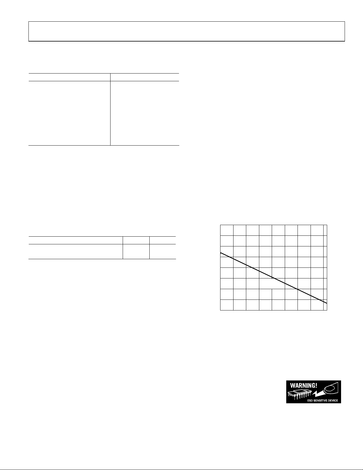
Figure 3 shows the maximum safe power dissipation in the
package versus the ambient temperature for the exposed paddle
(EP) SOIC-8 (θ
70°C/W) on a JEDEC standard 4-layer board. θ
approximations.
4.0
3.5
3.0
2.5
2.0
1.5
1.0
MAXIMUM POWER DISSIPATION (W)
0.5
0
–40 –20 0 20 40 60 80 100 120
performance of the AD8139. Exceeding a junction temperature of
175°C for an extended period of time can result in changes in the
silicon devices potentially causing failure.
Figure 3. Maximum Power Dissipation vs. Temperature for a 4-Layer Board
). The load current consists of differential
S
. Also, more metal directly in contact with
JA
.
JA
= 70°C/W) package and LFCSP (θJA =
JA
SOIC
AND LFCSP
AMBIENT TEMPERATURE (°C)
) is the sum of the
D
) times the
S
values are
JA
04679-0-055
ESD CAUTION
ESD (electrostatic discharge) sensitive device. Electrostatic charges as high as 4000 V readily accumulate on the
human body and test equipment and can discharge without detection. Although this product features proprietary ESD protection circuitry, permanent damage may occur on devices subjected to high energy electrostatic
discharges. Therefore, proper ESD precautions are recommended to avoid performance degradation or loss of
functionality.
Rev. A | Page 7 of 24
Page 8
AD8139
PIN CONFIGURATION AND FUNCTION DESCRIPTIONS
AD8139
–IN
1
2
V
OCM
V+
3
+OUT
4
NC = NO CONNECT
Figure 4. Pin Configuration
Table 5. Pin Function Descriptions
Pin No. Mnemonic Description
1 −IN Inverting Input.
2 V
OCM
An internal feedback loop drives the output common-mode voltage to be equal to the
voltage applied to the V
pin, provided the amplifier’s operation remains linear.
OCM
3 V+ Positive Power Supply Voltage.
4 +OUT Positive Side of the Differential Output.
5 −OUT Negative Side of the Differential Output.
6 V− Negative Power Supply Voltage.
7 NC No Internal Connection.
8 +IN Noninverting Input.
8
7
6
5
+IN
NC
V–
–OUT
R
F
04679-0-003
TEST
SIGNAL
SOURCE
V
TEST
SIGNAL
SOURCE
TEST
V
TEST
50Ω
60.4Ω
60.4Ω
50Ω
V
OCM
RG= 200Ω
RG= 200Ω
Figure 5. Basic Test Circuit
50Ω
60.4Ω
60.4Ω
50Ω
V
RG= 200Ω
OCM
RG= 200Ω
Figure 6. Capacitive Load Test Circuit, G = +1
AD8139
= 200Ω
R
F
AD8139
RF= 200Ω
C
F
R
L, dm
C
F
R
F
R
S
C
R
S
–
V
= 1kΩ
O, dm
+
L, dmRL, dm
04679-0-072
–
V
O, dm
+
04679-0-075
Rev. A | Page 8 of 24
Page 9

AD8139
TYPICAL PERFORMANCE CHARACTERISTICS
Unless otherwise noted, Diff. Gain = +1, RG = RF = 200 Ω, R
Figure 5 for the definition of terms.
2
1
0
–1
–2
–3
–4
–5
–6
–7
–8
–9
–10
–11
NORMALIZED CLOSED-LOOP GAIN (dB)
RG = 200Ω
–12
–13
= 0.1V p-p
V
O, dm
1 10 100 1000
G = 10
FREQUENCY (MHz)
Figure 7. Small Signal Frequency Response for Various Gains
5
4
3
2
1
0
–1
–2
–3
–4
–5
–6
CLOSED-LOOP GAIN (dB)
–7
–8
–9
V
= 0.1V p-p
O, dm
–10
10 100 1000
FREQUENCY (MHz)
VS =±5V
Figure 8. Small Signal Frequency Response for Various Power Supplies
3
2
1
0
–1
–2
–3
–4
–5
–6
–7
–8
CLOSED-LOOP GAIN (dB)
–9
–10
–11
V
= 0.1V p-p
O, dm
–12
10 100 1000
FREQUENCY (MHz)
Figure 9. Small Signal Frequency Response at Various ΩTemperatures
G = 2
G = 5
V
S
+125°C
+25°C
G = 1
= +5V
+85°C
–40°C
= 1 kΩ, VS = ±5 V, TA = 25°C, V
L, dm
2
1
0
–1
–2
–3
–4
–5
–6
–7
–8
–9
–10
–11
RG = 200Ω
NORMALIZED CLOSED-LOOP GAIN (dB)
–12
04679-0-004
V
–13
1 10 100 1000
Figure 10. Large Signal Frequency Response for Various Gains
3
2
1
0
–1
–2
–3
–4
–5
–6
–7
–8
CLOSED-LOOP GAIN (dB)
–9
–10
–11
04679-0-005
V
–12
10 100 1000
Figure 11. Large Signal Frequency Response for Various Power Supplies
3
2
1
0
–1
–2
–3
–4
–5
–6
–7
–8
CLOSED-LOOP GAIN (dB)
–9
–10
–11
04679-0-006
V
–12
10 100 1000
Figure 12. Large Signal Frequency Response at Various Temperatures
O, dm
O, dm
O, dm
OCM
= 2.0V p-p
= 2.0V p-p
= 2.0V p-p
= 0 V. Refer to the basic test circuit in
G = 1
G = 2G = 5
G = 10
04679-0-007
FREQUENCY (MHz)
VS =±5V
= +5V
V
S
04679-0-008
FREQUENCY (MHz)
+125°C +85°C
–40°C
FREQUENCY (MHz)
+25°C
04679-0-009
Rev. A | Page 9 of 24
Page 10

AD8139
3
2
1
0
–1
–2
–3
–4
–5
–6
–7
–8
CLOSED-LOOP GAIN (dB)
–9
–10
–11
V
= 0.1V p-p
O, dm
–12
10 100 1000
Figure 13. Small Signal Frequency Response for Various Loads
3
2
1
0
–1
–2
–3
–4
–5
–6
–7
–8
CLOSED-LOOP GAIN (dB)
–9
–10
–11
V
= 0.1V p-p
O, dm
–12
10 100 1000
Figure 14. Small Signal Frequency Response for Various C
6
5
4
3
2
1
0
–1
–2
–3
–4
–5
CLOSED-LOOP GAIN (dB)
–6
–7
–8
V
= 0.1V p-p
O, dm
–9
10 100 1000
Figure 15. Small Signal Frequency Response at Various V
= 200Ω
R
L
FREQUENCY (MHz)
C
= 2pF
F
FREQUENCY (MHz)
V
= +4.3V
OCM
= –4.3V
V
OCM
V
OCM
FREQUENCY (MHz)
RL = 1kΩ
= 0V
RL = 100Ω
= 0pF
C
F
CF = 1pF
V
= +4V
OCM
V
OCM
R
L
= –4V
= 500Ω
OCM
2
1
0
–1
RL = 100Ω
R
L
= 500Ω
–2
–3
–4
–5
–6
–7
–8
–9
CLOSED-LOOP GAIN (dB)
–10
R
= 1kΩ
L
–11
04679-0-040
O, dm
–13
10 100 1000
FREQUENCY (MHz)
R
L
= 200Ω
04679-0-041
–12
V
= 2.0V p-p
Figure 16. Large Signal Frequency Response for Various Loads
2
1
0
–1
–2
–3
–4
–5
–6
–7
–8
–9
CLOSED-LOOP GAIN (dB)
–10
–11
–12
V
= 2.0V p-p
04679-0-011
O, dm
–13
10 100 1000
F
04679-0-012
Figure 17. Large Signal Frequency Response for Various C
0.5
0.4
0.3
0.2
0.1
0
–0.1
–0.2
–0.3
NORMALIZED CLOSED-LOOP GAIN (dB)
–0.4
–0.5
1 10 100
CF = 0pF
C
= 2pF
F
FREQUENCY (MHz)
(V
O, dm
R
L
= 2.0V p-p)
(V
O, dm
R
= 2.0V p-p)
(V
O, dm
FREQUENCY (Hz)
C
= 1pF
F
RL = 100Ω
= 0.1V p-p)
= 100Ω
= 1kΩ
L
(V
O, dm
RL = 1kΩ
= 0.1V p-p)
04679-0-014
F
04679-0-042
Figure 18. 0.1 dB Flatness for Various Loads and Output Amplitudes
Rev. A | Page 10 of 24
Page 11

AD8139
–30
V
= 2.0V p-p
O, dm
–40
–50
–60
–70
–80
–90
DISTORTION (dBc)
–100
–110
–120
–130
0.1 1 10 100
FREQUENCY (MHz)
V
=±5V
S
VS = +5V
04679-0-015
Figure 19. Second Harmonic Distortion vs. Frequency and Supply Voltage
–30
V
= 2.0V p-p
O, dm
–40
–50
–60
–70
–80
–90
–100
DISTORTION (dB)
–110
–120
–130
–140
0.1 1 10 100
G = 5
FREQUENCY (MHz)
G = 1
G = 2
04679-0-016
Figure 20. Second Harmonic Distortion vs. Frequency and Gain
–30
V
= 2.0V p-p
O, dm
–40
–50
–60
–70
–80
–90
DISTORTION (dBc)
–100
–110
–120
–130
0.1 1 10 100
RL = 100Ω
= 200Ω
R
L
R
= 1kΩ
L
FREQUENCY (MHz)
R
L
= 500Ω
04679-0-017
Figure 21. Second Harmonic Distortion vs. Frequency and Load
–30
V
= 2.0V p-p
O, dm
–40
–50
–60
–70
–80
–90
DISTORTION (dBc)
–100
–110
–120
–130
0.1 1 10 100
FREQUENCY (MHz)
VS = +5V
V
=±5V
S
04679-0-018
Figure 22. Third Harmonic Distortion vs. Frequency and Supply Voltage
–30
V
= 2.0V p-p
O, dm
–40
–50
–60
–70
–80
–90
–100
DISTORTION (dB)
–110
–120
–130
–140
DISTORTION (dBc)
–100
–110
–120
–130
G = 1
0.1 1 10 100
G = 2
G = 5
FREQUENCY (MHz)
Figure 23. Third Harmonic Distortion vs. Frequency and Gain
–30
V
= 2.0V p-p
O, dm
–40
–50
–60
–70
–80
–90
0.1 1 10 100
FREQUENCY (MHz)
R
L
R
L
RL = 100Ω
= 200Ω
= 1kΩ
R
L
= 500Ω
04679-0-019
04679-0-020
Figure 24. Third Harmonic Distortion vs. Frequency and Load
Rev. A | Page 11 of 24
Page 12

AD8139
–30
V
= 2.0V p-p
O, dm
–40
–50
–60
–70
–80
–90
DISTORTION (dBc)
–100
–110
–120
–130
0.1 1 10 100
Figure 25. Second Harmonic Distortion vs. Frequency and R
–80
FC = 2MHz
–90
–100
–110
RF = 200Ω
R
= 500Ω
F
R
= 1kΩ
F
FREQUENCY (MHz)
V
S
V
=±5V
= +5V
S
F
04679-0-021
–30
V
= 2.0V p-p
O, dm
–40
–50
–60
–70
–80
–90
DISTORTION (dBc)
–100
–110
–120
–130
0.1 1 10 100
RF = 200
Ω
RF = 1k
Ω
FREQUENCY (MHz)
RF = 500
Ω
Figure 28. Third Harmonic Distortion vs. Frequency and R
–80
FC = 2MHz
–90
–100
–110
VS = +5V
VS =±5V
04679-0-024
F
–120
DISTORTION (dBc)
–130
–140
–150
012345678
V
O, dm
(V p-p)
Figure 26. Second Harmonic Distortion Vs. Output Amplitude
–60
–70
–80
–90
–100
DISTORTION (dBc)
–110
–120
–130
0 0.5 1.0 1.5 2.0 2.5 3.0 3.5 4.0 4.5 5.0
Figure 27. Harmonic Distortion vs. V
V
F
O, dm
C
= 2MHz
= 2V p-p
SECOND HARMONIC
THIRD HARMONIC
V
(V)
OCM
, VS = +5 V
OCM
04679-0-022
04679-0-023
–120
DISTORTION (dBc)
–130
–140
–150
087654321
V
O, dm
(V p-p)
Figure 29. Third Harmonic Distortion vs. Output Amplitude
–60
–70
–80
–90
–100
DISTORTION (dBc)
–110
–120
–130
–5 –4 –3 –2 –0 0 1 2 3 4 5
V
O, dm
= 2MHz
F
C
= 2V p-p
SECOND HARMONIC
THIRD HARMONIC
V
OCM
(V)
Figure 30. Harmonic Distortion vs. V
, VS = ±5 V
OCM
04679-0-025
04679-0-026
Rev. A | Page 12 of 24
Page 13

AD8139
100
V
= 100mV p-p
O, dm
75
50
(V)
O, dm
V
–100
–25
–50
–75
CF = 0pF
= 0pF,
(C
F
25
V
=±5V)
S
0
V
O, dm
(CF = 2pF, VS =±5V)
TIME (ns)
5ns/DIV
Figure 31. Small Signal Transient Response for Various C
(V)
O, dm
V
–0.025
–0.050
–0.075
–0.100
0.100
0.075
0.050
0.025
0
RS = 31.6
C
= 30pF
L, dm
= 63.4
R
S
C
= 15pF
L, dm
Ω
Ω
5ns/DIV
TIME (ns)
Figure 32. Small Signal Transient Response for Capacitive Loads
5
V
= 2V p-p
O, dm
0
1 = 10MHz
F
C
–5
2 = 10.1MHz
F
C
–10
–15
–20
–25
–30
–35
–40
–45
–50
–55
–60
–65
–70
–75
NORMALIZED OUTPUT (dBc)
–80
–85
–90
–95
–100
9.55 9.65 9.75 9.85 9.95 10.05 10.15 10.25 10.35 10.45 10.55
FREQUENCY (MHz)
Figure 33. Intermodulation Distortion
04679-0-043
F
04679-0-064
04679-0-027
2.5
(V)
O, dm
V
–0.5
–1.0
–1.5
–2.0
–2.5
2.0
1.5
1.0
0.5
CF = 0pF
C
= 2pF
F
C
= 0pF
F
= 2pF
C
F
0
4V p-p
2V p-p
5ns/DIV
TIME (ns)
Figure 34. Large Signal Transient Response For C
(V)
O, dm
V
1.5
1.0
0.5
0
–0.5
–1.0
–1.5
RS = 63.4
C
L, dm
= 31.6
R
S
C
L, dm
Ω
= 15pF
Ω
= 30pF
TIME (ns)
5ns/DIV
Figure 35. Large Signal Transient Response for Capacitive Loads
1.5
1.0
0.5
0
AMPLITUDE (V)
–0.5
–1.0
–1.5
V
O, dm
V
IN
TIME (ns)
CF = 2pF
V
O, dm
ERROR
= 2.0V p-p
35ns/DIV
Figure 36. Settling Time (0.01%)
04679-0-044
F
04679-0-065
600
400
200
0
–200
ERROR (µV) 1DIV = 0.01%
–400
04679-0-034
–600
Rev. A | Page 13 of 24
Page 14

AD8139
1.5
1.0
0.5
(V)
0
OCM
V
–0.5
–1.0
–1.5
0
V
INPUT CMRR =
–10
–20
–30
–40
–50
CMRR (dB)
–60
–70
–80
–90
1 10 100 500
100
±
5V
V
O, cm
V
IN, dm
Figure 37. V
= 0.2V p-p
IN, cm
Large Signal Transient Response
OCM
∆
V
O, cm
RF = RG = 10k
FREQUENCY (MHz)
Figure 38. CMRR vs. Fre quency
+5V
= 2V p-p
= 0V
TIME (ns)
/∆V
IN, cm
Ω
RF = RG = 200
6
5
4
3
2
1
0
–1
–2
–3
V
= 2.0V p-p
O, cm
–4
–5
CLOSED-LOOP GAIN (dB)
–6
10ns/DIV
04679-0-069
–7
–8
–9
10 100 1000
Figure 40. V
0
V
V
–10
–20
–30
–40
–50
CMRR (dB)
OCM
V
–60
Ω
04679-0-066
–70
–80
–90
1 10 100 500
O, cm
CMRR =∆V
OCM
VS = +5V
Frequency Response for Various Supplies
OCM
= 0.2V p-p
O, dm
Figure 41. V
100
VS = +5V
V
O, cm
V
=±5V VS =±5V
S
FREQUENCY (MHz)
/∆V
O, cm
FREQUENCY (MHz)
CMRR vs. Frequency
OCM
= 0.1V p-p
04679-0-038
04679-0-045
10
INPUT VOLTAGE NOISE (nV/ Hz)
1
10 100 1k 10k 100k 1M 10M 1G100M
FREQUENCY (Hz)
Figure 39. Input Voltage No ise vs. Frequency
04679-0-079
Rev. A | Page 14 of 24
10
NOISE (nV/ Hz)
OCM
V
1
10 100 1k 10k 100k 1M 10M 1G100M
Figure 42. V
FREQUENCY (Hz)
Voltage Noise vs. Frequency
OCM
04679-0-080
Page 15

AD8139
0
R
= 1k
Ω
L, dm
PSRR =∆V
–10
–20
–30
–40
–50
–60
PSRR (dB)
–70
–80
–90
–100
1 10 100 500
O, dm
/∆V
S
–PSRR
+PSRR
FREQUENCY (MHz)
Figure 43. PSRR v s. Frequency
100
VS = +5V
04679-0-047
14
G = 2
12
10
8
6
4
2
0
–2
VOLTAGE (V)
–4
–6
–8
–10
–12
–14
0
V
O, dm
OUTPUT BALANCE =
–10
TIME (ns)
Figure 46. Overdrive Recovery
= 1V p-p
∆
V
/∆V
O, cm
2× V
O, dm
IN, dm
V
O, dm
50ns/DIV
04679-0-046
10
)
Ω
V
1
OUTPUT IMPEDANCE (
0.1
0.01
0.1 1 10 100 1000
FREQUENCY (MHz)
Figure 44. Single-Ended Output Impedance vs. Frequency
700
600
500
400
300
200
100
0
V
=±5V
S
–100
–200
–300
–400
–500
–600
SINGLE-ENDED OUTPUT SWING FROM RAIL (mV)
–700
100 1k 10k
VS = +5V
RESISTIVE LOAD (Ω)
VS+– V
VON– V
OP
S–
Figure 45. Output Saturation Voltage vs. Output Load
=±5V
S
04679-0-028
04679-0-068
–20
–30
–40
–50
OUTPUT BALANCE (dB)
–60
–70
–80
1 10 100 500
FREQUENCY (MHz)
Figure 47. Output Balance vs. Frequency
300
VS = ±5V
G = 1 (RF = RG = 200Ω)
= 1kΩ
R
L, dm
250
200
150
SWING FROM RAIL (mV)
OP
V
100
50
–40 120100806040200–20
VS+– V
OP
VON– V
TEMPERATURE (°C)
S–
Figure 48. Output Saturation Voltage vs. Temperature
04679-0-067
–50
–100
–150
–200
SWING FROM RAIL (mV)
ON
V
–250
04679-0-077
–300
Rev. A | Page 15 of 24
Page 16

AD8139
3.0
(µA)
2.0
BIAS
I
1.5
I
BIAS
170
I
OS
1452.5
120
(nA)
OS
I
95
26
25
24
23
22
SUPPLY CURRENT (mA)
21
VS =±5V
VS = +5V
1.0
–40 –20 0 20 40 60 80 100 120
TEMPERATURE (°C)
Figure 49. Input Bias and Offset Current vs. Temperature
10
8
6
VS =±5V
4
2
0
–2
–4
INPUT BIAS CURRENT (µA)
–6
–8
–10
–5 –4 –3 –2 –1 0 1 2 3 4 5
V
ACM
(V)
V
= +5V
S
Figure 50. Input Bias Current vs.
Input Common-Mode Voltage
5
(V)
OUT, cm
V
4
3
2
1
0
–1
–2
–3
–4
–5
–5 543210–1–2–3–4
Figure 51. V
O, cm
vs. V
V
(V)
OCM
OCM
VS =±2.5V
Input Voltage
V
=±5V
S
70
04679-0-062
04679-0-073
04679-0-048
20
–40 –20 0 20 40 60 80 100 120
TEMPERATURE (°C)
Figure 52. Supply Current vs. Temperature
300
V
V
OS, dm
OS, cm
TEMPERATURE (°C)
250
200
(µV)
150
OS, dm
V
100
50
0
–40 –20 0 20 40 60 80 100 120
Figure 53. Offset Voltage vs. Temperature
50
COUNT = 350
MEAN = –50µV
45
STD DEV = 100µV
40
35
30
25
20
FREQUENCY
15
10
5
0
–500
–450
–400
–350
–300
–250
–200
Figure 54. V
–150
–50
–100
V
OS, dm
Distribution
OS, dm
0
50
(µV)
100
150
200
250
300
350
400
450
600
400
200
0
–200
–400
–600
500
04679-0-060
(µV)
OS, cm
V
04679-0-061
04679-0-071
Rev. A | Page 16 of 24
Page 17

AD8139
1.7
1.6
1.5
1.4
1.3
(µA)
1.2
VOCM
I
1.1
1.0
0.9
0.8
0.7
–40 –20 0 20 40 60 80 100 120
Figure 55. V
TEMPERATURE (°C)
Bias Current vs. Temperature
OCM
04679-0-063
6
4
VS =±5V
–5 –4 –3 –2 –1 0 1 2 3 4 5
Figure 56. V
OCM
V
(V)
OCM
Bias Current vs. V
CURRENT (µA)
OCM
V
2
0
–2
–4
–6
V
= +5V
S
Input Voltage
OCM
04679-0-074
Rev. A | Page 17 of 24
Page 18

AD8139
V
=
V
THEORY OF OPERATION
The AD8139 is a high speed, low noise differential amplifier
fabricated on the Analog Devices second generation eXtra Fast
Complementary Bipolar (XFCB) process. It is designed to
provide two closely balanced differential outputs in response to
either differential or single-ended input signals. Differential
gain is set by external resistors, similar to traditional voltagefeedback operational amplifiers. The common-mode level of the
output voltage is set by a voltage at the V
pendent of the input common-mode voltage. The AD8139 has
an H-bridge input stage for high slew rate, low noise, and low
distortion operation and rail-to-rail output stages that provide
maximum dynamic output range. This set of features allows for
convenient single-ended-to-differential conversion, a common
need to take advantage of modern high resolution ADCs with
differential inputs.
TYPICAL CONNECTION AND DEFINITION OF TERMS
Figure 57 shows a typical connection for the AD8139, using
matched external R
terminals of the AD8139, V
junctions. An external reference voltage applied to the V
terminal sets the output common-mode voltage. The two
output terminals, V
balanced fashion in response to an input signal.
networks. The differential input
F/RG
and VAN, are used as summing
AP
and VON, move in opposite directions in a
OP
C
F
pin and is inde-
OCM
OCM
balanced differential outputs of identical amplitude and exactly
180 degrees out of phase. The output balance performance does not
require tightly matched external components, nor does it require
that the feedback factors of each loop be equal to each other. Low
frequency output balance is limited ultimately by the mismatch
of an on-chip voltage divider, which is trimmed for optimum
performance.
Output balance is measured by placing a well matched resistor
divider across the differential voltage outputs and comparing
the signal at the divider’s midpoint with the magnitude of the
differential output. By this definition, output balance is equal to
the magnitude of the change in output common-mode voltage
divided by the magnitude of the change in output differentialmode voltage:
Δ
V
BalanceOutput
cmO,
= (3)
Δ
V
dmO,
The block diagram of the AD8139 in Figure 58 shows the
external differential feedback loop (R
differential input transconductance amplifier, G
networks and the
F/RG
DIFF
) and the
internal common-mode feedback loop (voltage divider across
V
and VON and the common-mode input transconductance
OP
amplifier, G
voltages at the summing junctions V
). The differential negative feedback drives the
CM
and VAP to be essentially
AN
equal to each other.
R
V
OCM
V
R
G
IP
R
G
IN
V
V
AP
AN
F
+
AD8139
–
R
F
C
F
V
ON
R
L, dm
V
OP
V
O, dm
–
+
04679-0-050
Figure 57. Typical Connection
The differential output voltage is defined as
(1)
VVV −=
dmO,
ONOP
Common-mode voltage is the average of two voltages. The
output common-mode voltage is defined as
VVV+
ONOP
=
cmO,
(2)
2
Output Balance
Output balance is a measure of how well VOP and VON are
matched in amplitude and how precisely they are 180 degrees
out of phase with each other. It is the internal common-mode
feedback loop that forces the signal component of the output
common-mode towards zero, resulting in the near perfectly
VV
(4)
APAN
The common-mode feedback loop drives the output commonmode voltage, sampled at the midpoint of the two 500 Ω resistors,
to equal the voltage set at the V
V
VV +=
OCMOP
dmO,
2
terminal. This ensures that
OCM
(5)
and
V
VV −=
OCMON
R
G
IN
V
AN
V
AP
V
IP
R
G
dmO,
(6)
2
+
G
DIFF
MIDSUPPLY
+
Figure 58. Block Diagram
10pF
G
G
G
10pF
R
F
O
CM
O
R
F
500Ω
500Ω
V
OP
V
OCM
V
ON
04679-0-051
Rev. A | Page 18 of 24
Page 19

AD8139
−=−
===
APPLICATIONS
R
ESTIMATING NOISE, GAIN, AND BANDWIDTH
WITH MATCHED FEEDBACK NETWORKS
Estimating Output Noise Voltage
The total output noise is calculated as the root-sum-squared
total of several statistically independent sources. Since the
sources are statistically independent, the contributions of each
must be individually included in the root-sum-square calculation. Table 6 lists recommended resistor values and estimates of
bandwidth and output differential voltage noise for various
closed-loop gains. For most applications, 1% resistors are
sufficient.
Table 6. Recommended Values of Gain-Setting Resistors and
Voltage Noise for Various Closed-Loop Gains
3 dB
Bandwidth
Gain RG (Ω) RF (Ω)
(MHz)
1 200 200 400 5.8
2 200 400 160 9.3
5 200 1 k 53 19.7
10 200 2 k 26 37
The differential output voltage noise contains contributions
from the AD8139’s input voltage noise and input current noise
as well as those from the external feedback networks.
The contribution from the input voltage noise spectral density
is computed as
Total Output
Noise (nV/√Hz)
The contribution from each
kTRnVo 44_ = (10)
F
Voltage Gain
The behavior of the node voltages of the single-ended-todifferential output topology can be deduced from the previous
definitions. Referring to Figure 57, (C
one can write
VV
IP
AP
R
G
R
⎡
==
VVV
OPAPAN
⎢
⎣
Solving the above two equations and setting VIP to Vi gives the
gain relationship for V
ONOP
O, dm/Vi
VVV ==−
dmO,
An inverting configuration with the same gain magnitude can
be implemented by simply applying the input signal to V
setting V
V
IN, dm
= 0. For a balanced differential input, the gain from
IP
to V
is also equal to RF/RG, where V
O, dm
Feedback Factor Notation
When working with differential amplifiers, it is convenient to
introduce the feedback factor β, which is defined as
is computed as
F
= 0) and setting VIN = 0
F
VV
ONAP
(11)
F
R
⎤
G
(12)
⎥
+
RR
F
G
⎦
.
R
F
V
(13)
i
R
G
and
IN
= VIP − VIN.
IN, dm
R
⎞
F
+=
, or equivalently, vn/β (7)
⎟
R
G
⎠
where
⎛
vVo_n 11
⎜
n
⎝
v
is defined as the input-referred differential voltage
n
noise. This equation is the same as that of traditional op amps.
The contribution from the input current noise of each input is
computed as
()
RiVo_n =2 (8)
n
F
where
i
is defined as the input noise current of one input. Each
n
input needs to be treated separately since the two input currents
are statistically independent processes.
The contribution from each
=
kTRVo_n 43
R
is computed as
G
R
⎞
⎛
F
(9)
⎟
⎜
G
R
G
⎠
⎝
This result can be intuitively viewed as the thermal noise of
each
R
multiplied by the magnitude of the differential gain.
G
Rev. A | Page 19 of 24
R
G
=β (14)
RR
+
F
G
This notation is consistent with conventional feedback analysis
and is very useful, particularly when the two feedback loops are
not matched.
Input Common-Mode Voltage
The linear range of the VAN and VAP terminals extends to within
approximately 1 V of either supply rail. Since V
and VAP are
AN
essentially equal to each other, they are both equal to the amplifier’s input common-mode voltage. Their range is indicated in
the Specifications tables as input common-mode range. The
voltage at V
and VAP for the connection diagram in Figure 57
AN
can be expressed as
VVV
ACMAPAN
where
R
⎛
F
⎜
+
RR
F
⎝
G
V
is the common-mode voltage present at the
ACM
+
)(
×
INIP
2
RVV
⎞
⎛
G
+
⎟
⎜
+
RR
F
⎠
⎝
G
⎞
×
V
(15)
⎟
OCM
⎠
amplifier input terminals.
Page 20

AD8139
(
)
β−+β
(
)
β
G
Using the β notation, Equation 15 can be written as
= 1 (16)
or equivalently,
+= (17)
V
where
ICM
is the common-mode voltage of the input signal, i.e.,
ICM
VVV+
INIP
=
.
2
For proper operation, the voltages at V
within their respective linear ranges.
Calculating Input Impedance
The input impedance of the circuit in Figure 57 will depend on
whether the amplifier is being driven by a single-ended or a
differential signal source. For balanced differential input signals,
the differential input impedance (
(18)
RR 2=
dmIN,
G
VVV
ICMOCMACM
VVVV −
ICMOCMICMACM
and VAP must stay
AN
R
) is simply
IN, dm
For a single-ended signal (for example, when V
and the input signal drives V
R
R
=
IN
G
R
1
F
−
RR
+
), the input impedance becomes
IP
(19)
)(2
F
is grounded
IN
The input impedance of a conventional inverting op amp
configuration is simply R
, but it is higher in Equation 19
G
because a fraction of the differential output voltage appears at
the summing junctions, V
and VAP. This voltage partially
AN
bootstraps the voltage across the input resistor RG, leading to
the increased input resistance.
Input Common-Mode Swing Considerations
In some single-ended-to-differential applications, when using a
single-supply voltage attention must be paid to the swing of the
input common-mode voltage, V
Consider the case in Figure 59, where
about a baseline at ground and
.
ACM
V
is 5 V p-p swinging
IN
V
is connected to ground.
REF
5V
+2.5V
GND
–2.5V
0.1µF 0.1µF 0.1µF
200Ω
V
OCM
2.5V
V
IN
V
REF
200Ω 324Ω
V
ACM
WITH V
REF
= 0
8
+
2
AD8139
1
–
324Ω
15Ω
3
5
4
6
+1.7V
+0.95V
+0.2V
15Ω
2.7nF
2.7nF
AVDD
IN–
IN+
DGND AGND REFGND REF REFBUFIN PDBUF
20Ω
DVDD
AD7674
0.1µF
Figure 59. AD8139 Driving AD7674, 18-Bit, 800 kSPS A/D Converter
47µF
ADR431
2.5V
REFERENCE
04679-0-052
Rev. A | Page 20 of 24
Page 21

AD8139
0
×∆=
The circuit has a differential gain of 1.6 and β = 0.38. V
ICM
has
an amplitude of 2.5 V p-p and is swinging about ground. Using
the results in Equation 16, the common-mode voltage at the
V
AD8139’s inputs,
baseline of 0.95 V. The maximum negative excursion of
, is a 1.5 V p-p signal swinging about a
ACM
V
in
ACM
this case is 0.2 V, which exceeds the lower input common-mode
voltage limit.
One way to avoid the input common-mode swing limitation is
to bias V
swinging about a baseline at 2.5 V and V
low-Z 2.5 V source. V
is swinging about 2.5 V. Using the results in Equation 17, V
calculated to be equal to
V
ACM
and V
IN
at midsupply. In this case, VIN is 5 V p-p
REF
is connected to a
REF
now has an amplitude of 2.5 V p-p and
ICM
V
because V
ICM
OCM
= V
. Therefore,
ICM
swings from 1.25 V to 3.75 V, which is well within the
ACM
is
input common-mode voltage limits of the AD8139. Another
benefit seen in this example is that since
V
= V
= V
OCM
ACM
ICM
no
wasted common-mode current flows. Figure 60 illustrates how
to provide the low-Z bias voltage. For situations that do not
require a precise reference, a simple voltage divider will suffice
to develop the input voltage to the buffer.
5V
This estimate assumes a minimum 90 degree phase margin for
the amplifier loop, which is a condition approached for gains
greater than 4. Lower gains will show more bandwidth than
predicted by the equation due to the peaking produced by the
lower phase margin.
Estimating DC Errors
Primary differential output offset errors in the AD8139 are due
to three major components: the input offset voltage, the offset
between the V
and VAP input currents interacting with the
AN
feedback network resistances, and the offset produced by the dc
voltage difference between the input and output common-mode
voltages in conjunction with matching errors in the feedback
network.
The first output error component is calculated as
RR
+
⎞
F
G
, or equivalently as VIO/β (21)
⎟
R
G
⎠
where V
⎛
VeVo 1_
=
⎜
IO
⎝
is the input offset voltage. The input offset voltage of the
IO
AD8139 is laser trimmed and guaranteed to be less than 500 μV.
The second error is calculated as
V
V TO 5V
0.1µF
10µF
0.1µF
200Ω
V
IN
OCM
200Ω 324Ω
0.1µF
+
Figure 60. Low-Z 2.5 V Buffer
8
+
2
AD8139
1
–
AD8031
324Ω
3
5
4
6
5V
+
–
TO AD7674 REFBUFIN
ADR431
2.5V
REFERENCE
04679-0-053
Another way to avoid the input common-mode swing limitation is to use dual power supplies on the AD8139. In this case,
the biasing circuitry is not required.
Bandwidth Versus Closed-Loop Gain
The AD8139’s 3 dB bandwidth decreases proportionally to
increasing closed-loop gain in the same way as a traditional
voltage feedback operational amplifier. For closed-loop gains
greater than 4, the bandwidth obtained for a specific gain can be
estimated as
R
G
VdBf
=−
dmOUT
,
×
RR
+
F
G
)300(,3
MHz
(20)
or equivalently, β(300 MHz).
where I
+
RR
⎛
F
=2_
IeVo =
⎜
IO
⎝
is defined as the offset between the two input bias
IO
G
R
G
RR
⎞
⎛
⎟
⎜
⎠
⎝
⎞
F
G
+
RR
F
G
()
RI
⎟
⎠
(22)
F
IO
currents.
The third error voltage is calculated as
)(3_
VVenreVo −
(23)
OCMICM
where Δ
enr is the fractional mismatch between the two
feedback resistors.
The total differential offset error is the sum of these three error
sources.
Other Impact of Mismatches in the Feedback Networks
The internal common-mode feedback network will still force
the output voltages to remain balanced, even when the R
F/RG
feedback networks are mismatched. The mismatch will,
however, cause a gain error proportional to the feedback
network mismatch.
Ratio-matching errors in the external resistors will degrade the
ability to reject common-mode signals at the V
and VIN input
AN
terminals, much the same as with a four-resistor difference
amplifier made from a conventional op amp. Ratio-matching
errors will also produce a differential output component that is
equal to the V
input voltage times the difference between the
OCM
feedback factors (βs). In most applications using 1% resistors,
this component amounts to a differential dc offset at the output
that is small enough to be ignored.
Rev. A | Page 21 of 24
Page 22

AD8139
Driving a Capacitive Load
A purely capacitive load will react with the bondwire and pin
inductance of the AD8139, resulting in high frequency ringing
in the transient response and loss of phase margin. One way to
minimize this effect is to place a small resistor in series with
each output to buffer the load capacitance, see Figure 6 and
Figure 61. The resistor and load capacitance will form a firstorder low-pass filter; therefore, the resistor value should be as
small as possible. In some cases, the ADCs require small series
resistors to be added on their inputs.
5
4
3
2
1
0
–1
–2
–3
–4
–5
–6
–7
–8
CLOSED LOOP GAIN (dB)
–9
VS =±5V
–10
V
= 0.1V p-p
O, dm
–11
G = 1 (R
= RG = 200Ω)
–12
–13
10M 100M 1G
F
R
= 1kΩ
L, dm
Figure 61. Frequency Response for
Various Capacitive Load and Series Resistance
RS = 30.1Ω
C
= 15pF
L
R
= 60.4Ω
S
C
= 15pF
L
= 60.4Ω
R
S
C
= 5pF
L
FREQUENCY (MHz)
The Typical Performance Characteristics that illustrate transient
response versus the capacitive load were generated using series
resistors in each output and a differential capacitive load.
Layout Considerations
Standard high speed PCB layout practices should be adhered to
when designing with the AD8139. A solid ground plane is recommended and good wideband power supply decoupling networks
should be placed as close as possible to the supply pins.
To minimize stray capacitance at the summing nodes, the
copper in all layers under all traces and pads that connect to the
summing nodes should be removed. Small amounts of stray
summing-node capacitance will cause peaking in the frequency
response, and large amounts can cause instability. If some stray
summing-node capacitance is unavoidable, its effects can be
compensated for by placing small capacitors across the feedback
resistors.
Terminating a Single-Ended Input
Controlled impedance interconnections are used in most high
speed signal applications, and they require at least one line
termination. In analog applications, a matched resistive
termination is generally placed at the load end of the line. This
section deals with how to properly terminate a single-ended
input to the AD8139.
= 30.1Ω
R
S
C
= 5pF
L
R
C
= 0Ω
S
L, dm
= 0pF
04679-0-076
The input resistance presented by the AD8139 input circuitry is
seen in parallel with the termination resistor, and its loading
effect must be taken into account. The Thevenin equivalent
circuit of the driver, its source resistance, and the termination
resistance must all be included in the calculation as well. An
exact solution to the problem requires the solution of several
simultaneous algebraic equations and is beyond the scope of
this data sheet. An iterative solution is also possible and simpler,
especially considering the fact that standard 1% resistor values
are generally used.
Figure 62 shows the AD8139 in a unity-gain configuration
driving the AD6645, which is a 14-bit high speed ADC, and
with the following discussion, provides a good example of how
to provide a proper termination in a 50 Ω environment.
The termination resistor, R
, in parallel with the 268 Ω input
T
resistance of the AD8139 circuit (calculated using Equation 19),
yields an overall input resistance of 50 Ω that is seen by the
signal source. In order to have matched feedback loops, each
loop must have the same R
if they have the same RF. In the
G
input (upper) loop, RG is equal to the 200 Ω resistor in series
with the (+) input plus the parallel combination of RT and the
source resistance of 50 Ω. In the upper loop, RG is therefore
equal to 228 Ω. The closest standard 1% value to 228 Ω is 226 Ω
and is used for R
in the lower loop. Greater accuracy could be
G
achieved by using two resistors in series to obtain a resistance
closer to 228 Ω.
Things get more complicated when it comes to determining the
feedback resistor values. The amplitude of the signal source
generator V
is two times the amplitude of its output signal
S
when terminated in 50 Ω. Thus, a 2 V p-p terminated amplitude
is produced by a 4 V p-p amplitude from V
equivalent circuit of the signal source and R
. The Thevenin
S
must be used
T
when calculating the closed-loop gain because in the upper loop
is split between the 200 Ω resistor and the Thevenin resis-
R
G
tance looking back toward the source. The Thevenin voltage of
the signal source is greater than the signal source output voltage
when terminated in 50 Ω because R
must always be greater
T
than 50 Ω. In this case, it is 61.9 Ω and the Thevenin voltage
and resistance are 2.2 V p-p and 28 Ω, respectively. Now the
upper input branch can be viewed as a 2.2 V p-p source in series
with 228 Ω. Since this is a unity-gain application, a 2 V p-p
differential output is required, and R
must therefore be 228 ×
F
(2/2.2) = 206 Ω. The closest standard value to this is 205 Ω.
When generating the Typical Performance Characteristics data,
the measurements were calibrated to take the effects of the
terminations on closed-loop gain into account.
Rev. A | Page 22 of 24
Page 23

AD8139
Since this is a single-ended-to-differential application on a
single supply, the input common-mode voltage swing must be
checked. From Figure 62, β = 0.52, V
1.1 V p-p swinging about ground. Using Equation 16,
= 2.4 V, and V
OCM
V
ICM
ACM
is
is
calculated to be 0.53 V p-p swinging about a baseline of 1.25 V,
and the minimum negative excursion is approximately 1 V.
Exposed Paddle (EP)
The SOIC-8 and LFCSP packages have an exposed paddle on
the underside of its body. In order to achieve the specified
thermal resistance, it must have a good thermal connection to one
of the PCB planes. The exposed paddle must be soldered to a pad
on top of the board that is connected to an inner plane with several
thermal vias.
5V 3.3V
0.01µF
205Ω 25Ω
2V p-p
50Ω
V
S
SIGNAL
SOURCE
R
61.9Ω
200Ω
V
T
OCM
226Ω
2.4V
Figure 62. AD8139 Driving AD6645,
3
8
+
2
AD8139
1
–
6
5
4
205Ω
25Ω
14-Bit, 80 MSPS/105 MSPS A/D Converter
AIN
AIN
AV
GND C1
0.01µF 0.01µF
CC
AD6645
C2 VREF
0.1µF
0.1µF
DV
CC
04679-0-054
Rev. A | Page 23 of 24
Page 24

AD8139
Y
R
OUTLINE DIMENSIONS
4.00 (0.157)
3.90 (0.154)
3.80 (0.150)
5.00 (0.197)
4.90 (0.193)
4.80 (0.189)
85
TOP VIEW
41
6.20 (0.244)
6.00 (0.236)
5.80 (0.228)
BOTTOM VIEW
(PINS UP)
2.29 (0.092)
2.29 (0.092)
1.27 (0.05)
BSC
0.25 (0.0098)
0.10 (0.0039)
COPLANARIT
0.10
CONTROLLING DIMENSIONS ARE IN MILLIMETERS; INCH DIMENSIONS
(IN PARENTHESES) ARE ROUNDED-OFF MILLIMETER EQUIVALENTS FOR
REFERENCE ONLY AND ARE NOT APPROPRIATE FOR USE IN DESIGN
SEATING
PLANE
COMPLIANT TO JEDEC STANDARDS MS-012
1.75 (0.069)
1.35 (0.053)
0.51 (0.020)
0.31 (0.012)
0.25 (0.0098)
0.17 (0.0068)
0.50 (0.020)
0.25 (0.010)
8°
1.27 (0.050)
0°
0.40 (0.016)
× 45°
Figure 63. 8-Lead Standard Small Outline Package with Exposed Pad [SOIC/EP], Narrow Body (RD-8-1)—Dimensions shown in millimeters and (inches)
0.50
0.40
PAD
0.30
4
1
1.60
1.45
1.30
1.50
REF
PIN 1
INDICATOR
1.90
1.75
1.60
PIN 1
INDICATO
0.90
0.85
0.80
SEATING
PLANE
12° MAX
3.00
BSC SQ
TOP
VIEW
0.30
0.23
0.18
0.80 MAX
0.65TYP
2.75
BSC SQ
0.20 REF
0.05 MAX
0.02 NOM
0.45
0.50
BSC
0.60 MAX
0.25
MIN
8
EXPOSED
(BOTTOMVIEW)
5
Figure 64. 8-Lead Lead Frame Chip Scale Package [LFCSP], 3 mm × 3 mm Body (CP-8-2)—Dimensions shown in millimeters
ORDERING GUIDE
Model Temperature Range Package Description Package Option Branding
AD8139ARD –40°C to +125°C 8-Lead Small Outline Package (SOIC) RD-8-1
AD8139ARD-REEL –40°C to +125°C 8-Lead Small Outline Package (SOIC) RD-8-1
AD8139ARD-REEL7 –40°C to +125°C 8-Lead Small Outline Package (SOIC) RD-8-1
AD8139ARDZ
AD8139ARDZ-REEL1 –40°C to +125°C 8-Lead Small Outline Package (SOIC) RD-8-1
AD8139ARDZ-REEL71 –40°C to +125°C 8-Lead Small Outline Package (SOIC) RD-8-1
AD8139ACP-R2 –40°C to +125°C 8-Lead Lead Frame Chip Scale Package (LFCSP) CP-8-2 HEB
AD8139ACP-REEL –40°C to +125°C 8-Lead Lead Frame Chip Scale Package (LFCSP) CP-8-2 HEB
AD8139ACP-REEL7 –40°C to +125°C 8-Lead Lead Frame Chip Scale Package (LFCSP) CP-8-2 HEB
AD8139ACPZ-R21 –40°C to +125°C 8-Lead Lead Frame Chip Scale Package (LFCSP) CP-8-2 HEB
AD8139ACPZ-REEL1 –40°C to +125°C 8-Lead Lead Frame Chip Scale Package (LFCSP) CP-8-2 HEB
AD8139ACPZ-REEL71 –40°C to +125°C 8-Lead Lead Frame Chip Scale Package (LFCSP) CP-8-2 HEB
1
Z = Pb-free part.
© 2004 Analog Devices, Inc. All rights reserved. Trademarks and registered trademarks are the property of their respective owners.
D04679–0–8/04(A)
1
–40°C to +125°C 8-Lead Small Outline Package (SOIC) RD-8-1
Rev. A | Page 24 of 24
 Loading...