

Page 1
Low Distortion
A
V
V
FEATURES
Adjustable output common-mode voltage
Low harmonic distortion
−94 dBc SFDR @ 5 MHz
−85 dBc SFDR @ 20 MHz
−3 dB bandwidth of 320 MHz, G = +1
Fast settling to 0.01% of 16 ns
Fast overdrive recovery of 4 ns
Low input voltage noise of 5 nV/√Hz
Low power 90 mW on 5 V
ENHANCED PRODUCT FEATURES
Supports defense and aerospace applications (AQEC)
Extended temperature range −55ºC to +105°C
Controlled manufacturing baseline
One assembly/test site
One fabrication site
Enhanced product change notification
Qualification data available on request
APPLICATIONS
ADC drivers
Single-ended-to-differential converters
IF and baseband gain blocks
Differential buffers
Line drivers
GENERAL DESCRIPTION
The AD8138-EP is a major advancement over op amps for
differential signal processing. The AD8138-EP can be used
as a single-ended-to-differential amplifier or as a differential-todifferential amplifier. The AD8138-EP is as easy to use as an op
amp and greatly simplifies differential signal amplification and
driving. Manufactured on Analog Devices, Inc., proprietary XFCB
bipolar process, the AD8138-EP has a −3 dB bandwidth of 320 MHz
and delivers a differential signal with the lowest harmonic distortion
available in a differential amplifier. The AD8138-EP has a unique
internal feedback feature that provides balanced output gain and
phase matching, suppressing even order harmonics. The internal
feedback circuit also minimizes any gain error that would be
associated with the mismatches in the external gain setting resistors.
Differential ADC Driver
AD8138-EP
PIN CONFIGURATION
D8138-EP
–IN
1
V
2
OCM
V+
3
+OUT
4
NC = NO CONNECT
Figure 1.
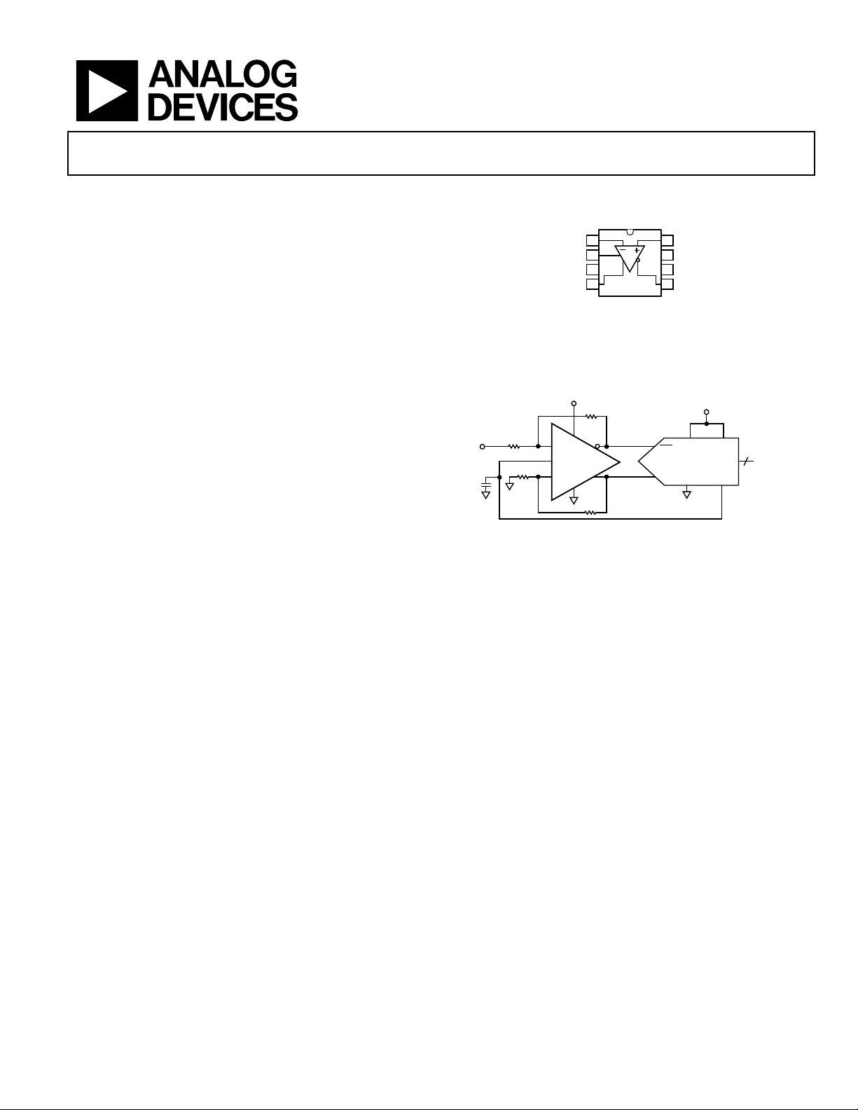
TYPICAL APPLICATION CIRCUIT
5
499Ω
499Ω
IN
The AD8138-EP’s differential output helps balance the input to
the differential ADCs, maximizing the performance of the ADC.
The AD8138-EP eliminates the need for a transformer with
high performance ADCs, preserving the low frequency and dc
information. The common-mode level of the differential output
is adjustable by a voltage on the V
the input signals for driving single-supply ADCs. Fast overload
recovery preserves sampling accuracy.
The AD8138-EP distortion performance makes it an ideal ADC
driver for communication systems, with distortion performance
good enough to drive state-of-the-art 10-bit to 16-bit converters
at high frequencies. The AD8138-EP’s high bandwidth and IP3 also
make it appropriate for use as a gain block in IF and baseband
signal chains. The AD8138-EP offset and dynamic performance
make it well suited for a wide variety of signal processing and
data acquisition applications. The AD8138-EP is available in the
MSOP package for operation over −55°C to +105°C temperatures.
Full details about this enhanced product are available in the
AD8138 data sheet, which should be consulted in conjunction
with this data sheet.
499Ω
V
OCM
+
AD8138-EP
–
499Ω
Figure 2.
+IN
8
NC
7
V–
6
–OUT
5
08997-001
5V
AVDD DVDD
AIN
ADC
AIN
pin, easily level-shifting
OCM
AVSS
V
REF
DIGITAL
OUTPUTS
08997-002
Rev. 0
Information furnished by Analog Devices is believed to be accurate and reliable. However, no
responsibility is assumed by Analog Devices for its use, nor for any infringements of patents or other
rights of third parties that may result from its use. Specifications subject to change without notice. No
license is granted by implication or otherwise under any patent or patent rights of Analog Devices.
Trademarks and registered trademarks are the property of their respective owners.
One Technology Way, P.O. Box 9106, Norwood, MA 02062-9106, U.S.A.
Tel: 781.329.4700 www.analog.com
Fax: 781.461.3113 ©2010 Analog Devices, Inc. All rights reserved.
Page 2

AD8138-EP
TABLE OF CONTENTS
Features .............................................................................................. 1
V
to ±OUT Specifications ......................................................6
OCM
Enhanced Product Features ............................................................ 1
Applications ....................................................................................... 1
General Description ......................................................................... 1
Pin Configuration ............................................................................. 1
Typical Application Circuit ............................................................. 1
Revision History ............................................................................... 2
Specifications ..................................................................................... 3
±DIN to ±OUT Specifications ...................................................... 3
V
to ±OUT Specifications ..................................................... 4
OCM
±DIN to ±OUT Specifications ...................................................... 5
REVISION HISTORY
4/10—Revision 0: Initial Version
Absolute Maximum Ratings ............................................................7
Thermal Resistance .......................................................................7
Maximum Power Dissipation ......................................................7
ESD Caution...................................................................................7
Maximum Output Voltage Swing ................................................8
Pin Configuration and Function Descriptions ..............................9
Outline Dimensions ....................................................................... 10
Ordering Guide .......................................................................... 10
Rev. 0 | Page 2 of 12
Page 3

AD8138-EP
SPECIFICATIONS
±DIN TO ±OUT SPECIFICATIONS
At 25°C, VS = ±5 V, V
differential outputs, unless otherwise noted.
Table 1.
Parameter Conditions Min Typ Max Unit
DYNAMIC PERFORMANCE
−3 dB Small Signal Bandwidth V
T
V
Bandwidth for 0.1 dB Flatness V
Large Signal Bandwidth V
Slew Rate V
Settling Time 0.01%, V
Overdrive Recovery Time VIN = 5 V to 0 V step, G = +2 4 ns
NOISE/HARMONIC PERFORMANCE
Second Harmonic V
V
V
Third Harmonic V
V
V
IMD 20 MHz −77 dBc
IP3 20 MHz 37 dBm
Voltage Noise (RTI) f = 100 kHz to 40 MHz 5 nV/√Hz
Input Current Noise f = 100 kHz to 40 MHz 2 pA/√Hz
INPUT CHARACTERISTICS
Offset Voltage V
T
Input Bias Current 3.5 7 μA
T
Input Resistance Differential 6 MΩ
Common mode 3 MΩ
Input Capacitance 1 pF
Input Common-Mode Voltage −4.7 to +3.4 V
CMRR ΔV
T
OUTPUT CHARACTERISTICS
Output Voltage Swing2 Maximum ΔV
Output Balance Error ΔV
1
Specified to ±6 sigma over the −55°C to +105°C operating temperature range.
2
Output swing capabilities vary over operating temperature. See for more information. Figure 4
= 0 V, G = +1, R
OCM
= 500 Ω, unless otherwise noted. All specifications refer to single-ended input and
L, dm
= 0.5 V p-p, CF = 0 pF 290 320 MHz
OUT
MIN
OUT
OUT
OUT
OUT
OUT
OUT
OUT
OUT
OUT
OUT
OS, dm
MIN
MIN
OUT, dm
MIN
OUT, cm
1
to T
256 MHz
MAX
= 0.5 V p-p, CF = 1 pF 225 MHz
= 0.5 V p-p, CF = 0 pF 30 MHz
= 2 V p-p, CF = 0 pF 265 MHz
= 2 V p-p, CF = 0 pF 1150 V/μs
= 2 V p-p, CF = 1 pF 16 ns
OUT
= 2 V p-p, 5 MHz, R
= 2 V p-p, 20 MHz, R
= 2 V p-p, 70 MHz, R
= 2 V p-p, 5 MHz, R
= 2 V p-p, 20 MHz, R
= 2 V p-p, 70 MHz, R
= V
to T
to T
to T
/2; V
OUT, dm
1
−4.8 +4.8 mV
MAX
variation −0.01 μA/°C
MAX
/ΔV
; ΔV
IN, cm
1
−69 dB
MAX
; single-ended output 7.75 V p-p
OUT
/ΔV
OUT, dm
; ΔV
= 800 Ω −94 dBc
L, dm
= 800 Ω −87 dBc
L, dm
= 800 Ω −62 dBc
L, dm
= 800 Ω −114 dBc
L, dm
= 800 Ω −85 dBc
L, dm
= 800 Ω −57 dBc
L, dm
= V
= V
DIN+
DIN−
= ±1 V, −77 −70 dB
IN, cm
= 1 V −66 dB
OUT, dm
= 0 V −2.5 ±1 +2.5 mV
OCM
Rev. 0 | Page 3 of 12
Page 4

AD8138-EP
V
TO ±OUT SPECIFICATIONS
OCM
At 25°C, VS = ±5 V, V
differential outputs, unless otherwise noted.
Table 2.
Parameter Conditions Min Typ Max Unit
DYNAMIC PERFORMANCE
−3 dB Bandwidth 250 MHz
Slew Rate 330 V/μs
INPUT VOLTAGE NOISE (RTI) f = 0.1 MHz to 100 MHz 17 nV/√Hz
DC PERFORMANCE
Input Voltage Range ±3.8 V
Input Resistance 200 kΩ
Input Offset Voltage V
T
Input Bias Current 0.5 μA
V
CMRR ΔV
OCM
Gain ΔV
POWER SUPPLY
Operating Range ±1.4 ±5.5 V
Quiescent Current 18 20 23 mA
T
Power Supply Rejection Ratio ΔV
OPERATING TEMPERATURE RANGE −55 +105 °C
1
Specified to ±6 sigma over the −55°C to +105°C operating temperature range.
= 0 V, G = +1, R
OCM
= 500 Ω, unless otherwise noted. All specifications refer to single-ended input and
L, dm
OS, cm
MIN
OUT, dm
OUT, cm
MIN
OUT, dm
= V
to T
to T
; V
= V
= V
OUT, cm
DIN+
1
−10.2 +10.2 mV
MAX
/ΔV
; ΔV
OCM
/ΔV
; ΔV
OCM
1
13.2 mA
MAX
DIN–
= ±1 V −75 dB
OCM
= ±1 V, T
OCM
/ΔVS; ΔVS = ±1 V, T
= 0 V −3.5 ±1 +3.5 mV
OCM
1
to T
0.9955 1 1.0045 V/V
MAX
1
−90 −70 dB
MIN
MIN
to T
MAX
Rev. 0 | Page 4 of 12
Page 5

AD8138-EP
±DIN TO ±OUT SPECIFICATIONS
At 25°C, VS = 5 V, V
differential output, unless otherwise noted.
Table 3.
Parameter Conditions Min Typ Max Unit
DYNAMIC PERFORMANCE
−3 dB Small Signal Bandwidth V
T
V
Bandwidth for 0.1 dB Flatness V
Large Signal Bandwidth V
Slew Rate V
Settling Time 0.01%, V
Overdrive Recovery Time VIN = 2.5 V to 0 V step, G = +2 4 ns
NOISE/HARMONIC PERFORMANCE
Second Harmonic V
V
V
Third Harmonic V
V
V
IMD 20 MHz −74 dBc
IP3 20 MHz 35 dBm
Voltage Noise (RTI) f = 100 kHz to 40 MHz 5 nV/√Hz
Input Current Noise f = 100 kHz to 40 MHz 2 pA/√Hz
INPUT CHARACTERISTICS
Offset Voltage V
T
Input Bias Current 3.5 7 μA
T
Input Resistance Differential 6 MΩ
Common mode 3 MΩ
Input Capacitance 1 pF
Input Common-Mode Voltage −0.3 to +3.2 V
CMRR ΔV
T
OUTPUT CHARACTERISTICS
Output Voltage Swing2 Maximum ∆V
Output Balance Error ΔV
1
Specified to ±6 sigma over the −55°C to +105°C operating temperature range.
2
Output swing capabilities vary over operating temperature. See for more information. Figure 5
= 2.5 V, G = +1, R
OCM
= 500 Ω, unless otherwise noted. All specifications refer to single-ended input and
L, dm
= 0.5 V p-p, CF = 0 pF 280 310 MHz
OUT
MIN
OUT
OUT
OUT
OUT
OUT
OUT
OUT
OUT
OUT
OUT
OS, dm
MIN
MIN
OUT, dm
MIN
OUT, cm
1
to T
242 MHz
MAX
= 0.5 V p-p, CF = 1 pF 225 MHz
= 0.5 V p-p, CF = 0 pF 29 MHz
= 2 V p-p, CF = 0 pF 265 MHz
= 2 V p-p, CF = 0 pF 950 V/μs
= 2 V p-p, CF = 1 pF 16 ns
OUT
= 2 V p-p, 5 MHz, R
= 2 V p-p, 20 MHz, R
= 2 V p-p, 70 MHz, R
= 2 V p-p, 5 MHz, R
= 2 V p-p, 20 MHz, R
= 2 V p-p, 70 MHz, R
= V
to T
to T
to T
/2; V
OUT, dm
1
−5.1 +5.1 mV
MAX
variation −0.01 μA/°C
MAX
/ΔV
; ΔV
IN, cm
1
−69.5 dB
MAX
; single-ended output 2.9 V p-p
OUT
/ΔV
OUT, dm
; ΔV
= 800 Ω −90 dBc
L, dm
= 800 Ω −79 dBc
L, dm
= 800 Ω −60 dBc
L, dm
= 800 Ω −100 dBc
L, dm
= 800 Ω −82 dBc
L, dm
= 800 Ω −53 dBc
L, dm
= V
= V
DIN+
DIN–
= 1 V −77 −70 dB
IN, cm
= 1 V −65 dB
OUT, dm
= 0 V −2.5 ±1 +2.5 mV
OCM
Rev. 0 | Page 5 of 12
Page 6

AD8138-EP
V
TO ±OUT SPECIFICATIONS
OCM
At 25°C, VS = 5 V, V
differential output, unless otherwise noted.
Table 4.
Parameter Conditions Min Typ Max Unit
DYNAMIC PERFORMANCE
−3 dB Bandwidth 220 MHz
Slew Rate 250 V/μs
INPUT VOLTAGE NOISE (RTI) f = 0.1 MHz to 100 MHz 17 nV/√Hz
DC PERFORMANCE
Input Voltage Range 1.0 to 3.8 V
Input Resistance 100 kΩ
Input Offset Voltage V
T
Input Bias Current 0.5 μA
V
CMRR ΔV
OCM
Gain ΔV
POWER SUPPLY
Operating Range 2.7 11 V
Quiescent Current 15 20 21 mA
T
Power Supply Rejection Ratio ΔV
T
OPERATING TEMPERATURE RANGE −55 +105 °C
1
Specified to ±6 sigma over the −55°C to +105°C operating temperature range.
= 2.5 V, G = +1, R
OCM
= 500 Ω, unless otherwise noted. All specifications refer to single-ended input and
L, dm
OS, cm
MIN
OUT, dm
OUT, cm
MIN
OUT, dm
MIN
= V
to T
to T
to T
; V
= V
= V
OUT, cm
DIN+
1
−9.7 +9.7 mV
MAX
/ΔV
; ΔV
OCM
/ΔV
; ΔV
OCM
1
10.6 mA
MAX
DIN–
= 2.5 V ± 1 V −70 dB
OCM
= 2.5 V ± 1 V, T
OCM
= 0 V −5 ±1 +5 mV
OCM
1
to T
MIN
0.9968 1 1.0032 V/V
MAX
/ΔVS; ΔVS = ± 1 V −90 −70 dB
1
−57 dB
MAX
Rev. 0 | Page 6 of 12
Page 7

AD8138-EP
ABSOLUTE MAXIMUM RATINGS
Table 5.
Parameter Rating
Supply Voltage ±5.5 V
V
±VS
OCM
Output Voltage Swing See Figure 4 and Figure 5
Internal Power Dissipation 550 mW
Operating Temperature Range −55°C to +105°C
Storage Temperature Range −65°C to +150°C
Lead Temperature (Soldering, 10 sec) 300°C
Junction Temperature 150°C
Stresses above those listed under Absolute Maximum Ratings
may cause permanent damage to the device. This is a stress
rating only; functional operation of the device at these or any
other conditions above those indicated in the operational
section of this specification is not implied. Exposure to absolute
maximum rating conditions for extended periods may affect
device reliability.
THERMAL RESISTANCE
θJA is specified for the worst-case conditions, that is, θJA is
specified for the device soldered in a circuit board in still air.
Table 6.
Package Type θJA Unit
8-Lead MSOP/4-Layer 145 °C/W
MAXIMUM POWER DISSIPATION
The maximum safe power dissipation in the AD8138-EP package
is limited by the associated rise in junction temperature (T
the die. At approximately 150°C, which is the glass transition
temperature, the plastic changes its properties. Even temporarily
exceeding this temperature limit can change the stresses that the
package exerts on the die, permanently shifting the parametric
performance of the AD8138-EP. Exceeding a junction temperature
of 150°C for an extended period can result in changes in the
silicon devices, potentially causing failure.
) on
J
The power dissipated in the package (P
) is the sum of the
D
quiescent power dissipation and the power dissipated in the
package due to the load drive for all outputs. The quiescent
power is the voltage between the supply pins (V
quiescent current (I
). The load current consists of the differential
S
) times the
S
and common-mode currents flowing to the load, as well as
currents flowing through the external feedback networks and
internal common-mode feedback loop. The internal resistor tap
used in the common-mode feedback loop places a negligible
differential load on the output. RMS voltages and currents should
be considered when dealing with ac signals.
Airflow reduces θ
. In addition, more metal directly in contact
JA
with the package leads from metal traces, through holes, ground,
and power planes reduces the θ
.
JA
Figure 3 shows the maximum safe power dissipation vs. the
ambient temperature for the 8-lead MSOP (θ
package on a JEDEC standard 4-layer board. θ
= 145°C/W)
JA
values are
JA
approximations.
1.75
1.50
1.25
1.00
0.75
0.50
MAXIMUM POWER DISSIPATION (W)
0.25
0
–55
–45
–35
–25
Figure 3. Maximum Power Dissipation vs. Ambient Temperature
5
152535
–5
–15
AMBIENT TEM PE RATURE (°C)
45
55
65
75
95
85
105
08997-003
ESD CAUTION
Rev. 0 | Page 7 of 12
Page 8

AD8138-EP
MAXIMUM OUTPUT VOLTAGE SWING
The maximum output voltage swing must be considered in order
for the AD8138-EP to remain current density compliant over
the extended temperature range. The maximum output swing
is dependent on the load resistance and operating temperatures.
Figure 4 shows the maximum output swing over operating
temperatures for various loads at ±5 V operation.
8
R
= 6.8kΩ
L
7
R
= 2kΩ
L
6
= 1kΩ
R
5
4
VS = ±5V
V
MAX = 7.75V p-p
3
25 105 11595857565554535
OUT
AMBIENT TEM P E RATURE (°C)
DIFFERENTIAL OUTPUT VOLTAGE SWING (V p-p)
Figu re 4. Differential Output Voltage Swing vs. Ambient Temperature, V
The following equation can be used to determine the maximum
output voltage swing for V
Output = (38.21 × ln(R
= ±5 V:
S
) − 169.26) ×
L
where:
Output is the maximum output voltage swing that cannot exceed
7.75 V p-p.
R
is the load resistance (Ω).
L
is the ambient temperature (°C).
T
A
L
R
L
Te×−
= 500Ω
)0293.0(
A
= ±5 V
S
08997-004
Figure 5 shows the maximum output swing over operating
temperatures for various loads at V
3
2.6
2.2
1.8
VS = 5V
V
MAX = 2.9V p-p
DIFFERENTIAL OUTPUT VOLTAGE SWING (V p-p)
Figure 5. Differential Output Voltage Swing vs. Ambient Temperature, V
OUT
1.4
25 35 45 55 65 75 85 95 105 115
AMBIENT TEM PE RATURE (°C)
= 5 V operation.
S
RL = 300Ω
R
R
R
= 200Ω
L
= 150Ω
L
= 100Ω
L
08997-005
= 5 V
S
The following equation can be used to determine the maximum
output voltage swing for V
Output = (24.36 × ln(R
= 5 V:
S
) − 82.34) ×
L
)028.0(
Te×−
A
where:
Output is the maximum output voltage swing that cannot exceed
2.9 V p-p.
R
is the load resistance (Ω).
L
is the ambient temperature (°C).
T
A
Rev. 0 | Page 8 of 12
Page 9

AD8138-EP
T
A
PIN CONFIGURATION AND FUNCTION DESCRIPTIONS
D8138-EP
–IN
1
V
2
OCM
V+
3
+OU
4
NC = NO CONNECT
Figure 6. Pin Configuration
Table 7. Pin Function Descriptions
Pin No. Mnemonic Description
1 −IN Negative Input Summing Node.
2 V
OCM
Voltage applied to this pin sets the common-mode output voltage with a ratio of 1:1. For example, 1 V dc on
V
sets the dc bias level on +OUT and −OUT to 1 V.
OCM
3 V+ Positive Supply Voltage.
4 +OUT Positive Output. Note that the voltage at −DIN is inverted at +OUT.
5 −OUT Negative Output. Note that the voltage at +DIN is inverted at –OUT.
6 V− Negative Supply Voltage.
7 NC No Connect.
8 +IN Positive Input Summing Node.
+IN
8
NC
7
V–
6
–OUT
5
08997-001
Rev. 0 | Page 9 of 12
Page 10

AD8138-EP
OUTLINE DIMENSIONS
3.20
3.00
2.80
8
5
3.20
3.00
2.80
PIN 1
IDENTIFIER
0.95
0.85
0.75
0.15
0.05
COPLANARITY
1
0.65 BSC
0.10
COMPLIANT TO JEDEC STANDARDS MO-187-AA
Figure 7. 8-Lead Mini Small Outline Package [MSOP]
5.15
4.90
4.65
4
15° MAX
6°
0°
0.23
0.09
0.40
0.25
1.10 MAX
(RM-8)
Dimensions shown in millimeters
0.80
0.55
0.40
100709-B
ORDERING GUIDE
Model1 Temperature Range Package Description Package Option Branding
AD8138SRMZ-EP-R7 −55°C to +105°C 8-Lead MSOP, 7" Tape and Reel RM-8 H27
1
Z = RoHS Compliant Part.
Rev. 0 | Page 10 of 12
Page 11

AD8138-EP
NOTES
Rev. 0 | Page 11 of 12
Page 12

AD8138-EP
NOTES
©2010 Analog Devices, Inc. All rights reserved. Trademarks and
registered trademarks are the property of their respective owners.
D08997-0-4/10(0)
Rev. 0 | Page 12 of 12
 Loading...