

Page 1
600 MHz, 32 × 32 Buffered
FEATURES
High channel count, 32 × 32 high speed, non-blocking
switch array
Differential or single-ended operation
Differential G = +1 (AD8117) or G = +2 (AD8118)
Flexible power supplies
Single +5 V supply, or dual ±2.5 V supplies
Serial or parallel programming of switch array
High impedance output disable allows connection of
multiple devices with minimal loading on output bus
Excellent video performance
>50 MHz 0.1 dB gain flatness
0.05%/0.05° differential gain/phase error (R
Excellent ac performance
Bandwidth: 600 MHz
Slew rate: 1800 V/μs
Settling time: 2.5 ns to 1%
Low power of 2.5 W
Low all hostile crosstalk
< −70 dB @ 5 MHz
< −43 dB @ 600 MHz
Reset pin allows disabling of all outputs (connected through
a capacitor to ground provides power-on reset capability)
304-ball BGA package (31 mm × 31 mm)
= 150 Ω)
L
SER/PAR
WE
CLK
DATA IN
UPDATE
RESET
32 INPUT PAIRS
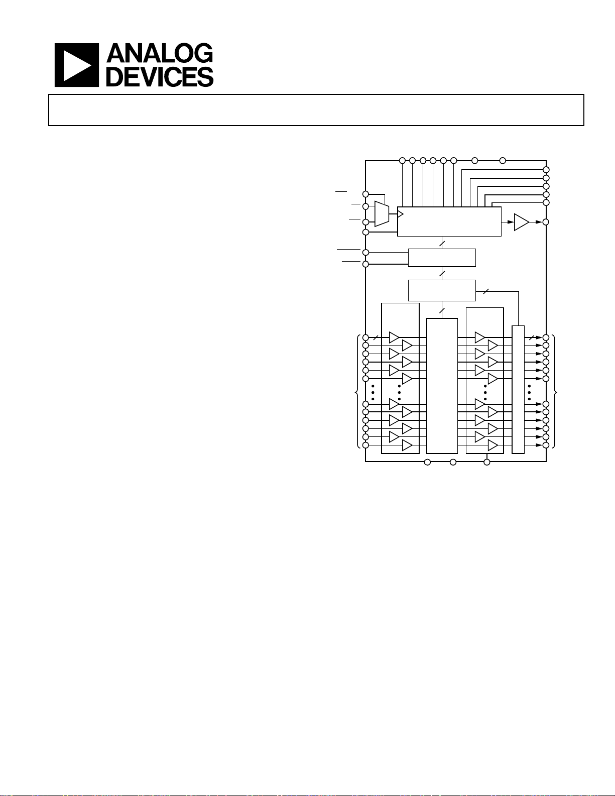
Analog Crosspoint Switch
AD8117/AD8118
FUNCTIONAL BLOCK DIAGRAM
D0 D1 D2 D3 D4 D5VDD DGND
AD8117/
AD8118
1
0
RECEIVER
G = +1*
G = +2**
192-BIT SHIFT REGISTER
WITH 6-BIT
PARALLEL LOADING
PARALLEL LATCH
DECODE
32 × 6:32 DECODERS
INPUT
SWITCH
MATRIX
192
192
1024
32
OUTPUT
BUFFER
G = +1
ENABLE/DISABLE
A0
A1
A2
A3
A4
DATA
OUT
SET INDIVIDUAL, OR
RESET ALL OUTPUTS TO OF F
22
32 OUTPUT PAIRS
APPLICATIONS
Routing of high speed signals including
RGB and component video routing
KVM
Compressed video (MPEG, wavelet)
Data communications
GENERAL DESCRIPTION
The AD8117/AD8118 are high speed, 32 × 32 analog crosspoint
switch matrices. They offer 600 MHz bandwidth and slew rate of
1800 V/µs for high resolution computer graphics (RGB) signal
switching. With less than −70 dB of crosstalk and −90 dB
isolation (@ 5 MHz), the AD8117/AD8118 are useful in many
high speed applications. The 0.1 dB flatness greater than
50 MHz makes the AD8117/AD8118 ideal for composite video
switching.
The AD8117/AD8118 include 32 independent output buffers
that can be placed into a high impedance state for paralleling
crosspoint outputs so that off-channels present minimal loading
to an output bus. The AD8117 has a differential gain of +1,
while the AD8118 has a differential gain of +2 for ease of use in
Rev. A
Information furnished by Analog Devices is believed to be accurate and reliable. However, no
responsibility is assumed by Anal og Devices for its use, nor for any infringements of patents or ot her
rights of third parties that may result from its use. Specifications subject to change without notice. No
license is granted by implication or otherwise under any patent or patent rights of Analog Devices.
Trademarks and registered trademarks are the property of their respective owners.
*AD8117 ONLY
**AD8118 ONLY
VPOS VNEG VOCM
Figure 1.
back-terminated load applications. They operate as fully
differential devices or can be configured for single-ended
operation. Either a single +5 V supply or dual ±2.5 V supplies
can be used, while consuming only 500 mA of idle current with
all outputs enabled. The channel switching is performed via a
double-buffered, serial digital control (which can accommodate
daisy chaining of several devices), or via a parallel control,
allowing updating of an individual output without reprogramming the entire array.
The AD8117/AD8118 are packaged in a 304-ball BGA package
and are available over the extended industrial temperature
range of −40°C to +85°C.
One Technology Way, P.O. Box 9106, Norwood, MA 02062-9106, U.S.A.
Tel: 781.329.4700 www.analog.com
Fax: 781.461.3113 ©2007 Analog Devices, Inc. All rights reserved.
06365-001
Page 2

AD8117/AD8118
TABLE OF CONTENTS
Features .............................................................................................. 1
Applications....................................................................................... 1
Functional Block Diagram .............................................................. 1
General Description......................................................................... 1
Revision History ............................................................................... 2
Specifications..................................................................................... 3
Timing Characteristics (Serial Mode) ....................................... 5
Timing Characteristics (Parallel Mode) .................................... 6
Absolute Maximum Ratings............................................................ 7
Thermal Resistance ...................................................................... 7
Power Dissipation......................................................................... 7
REVISION HISTORY
5/07—Rev. 0 to Rev. A
Added AD8118 ...................................................................Universal
Changes to Data Sheet Title ........................................................... 1
Changes to Table 1............................................................................ 3
2/07—Revision 0: Initial Version
ESD Caution...................................................................................7
Pin Configuration and Function Descriptions..............................8
Truth Ta b l e and L o gic D i agra m ............................................... 13
I/O Schematics................................................................................ 15
Typical Perf or m an c e Charac t e r istics ........................................... 17
Theory of Operation ...................................................................... 25
Applications..................................................................................... 26
Programming.............................................................................. 26
Operating Modes........................................................................ 27
Outline Dimensions ....................................................................... 36
Ordering Guide .......................................................................... 36
Rev. A | Page 2 of 36
Page 3

AD8117/AD8118
SPECIFICATIONS
VS = ±2.5 V at TA = 25°C, R
Table 1.
AD8117/AD8118
Parameter Conditions Min Typ Max Unit
DYNAMIC PERFORMANCE
−3 dB Bandwidth 200 mV p-p, typical channel
2 V p-p, typical channel 420/525 MHz
Gain Flatness 0.1 dB, 200 mV p-p 100/50 MHz
0.1 dB, 2 V p-p 70/50 MHz
Propagation Delay 2 V p-p 1.3 ns
Settling Time 1%, 2 V step 2.5 ns
Slew Rate 2 V step, peak 1800 V/µs
2 V step, 10% to 90% 1500 V/µs
NOISE/DISTORTION PERFORMANCE
Differential Gain Error NTSC or PAL, RL = 150 Ω 0.05 %
Differential Phase Error NTSC or PAL, RL = 150 Ω 0.05 Degrees
Crosstalk, All Hostile f = 5 MHz −70/−75 dB
f = 10 MHz −65/−70 dB
f = 100 MHz −45/−50 dB
f = 600 MHz −43/−50 dB
Off Isolation, Input-Output f = 10 MHz, one channel −90 dB
Input Voltage Noise 0.1 MHz to 50 MHz 45/53 nV/√Hz
DC PERFORMANCE
Voltage Gain Differential +1/+2 V/V
Gain Error ±1 %
No load ±1 ±3 %
Gain Matching Channel-to-channel ±1 %
Differential Offset ±5 ±25 mV
Common-Mode Offset ±25 ±90 mV
OUTPUT CHARACTERISTICS
Output Impedance DC, enabled 0.1 Ω
Disabled, differential 30 kΩ
Output Disable Capacitance Disabled 4 pF
Output Leakage Current Disabled 1 µA
Output Voltage Range No load 2.8 3.8 V p-p
V
Input Range V
OCM
V
Output Swing Limit Single-ended output −1.3 1.3 V
Output Current Maximum operating signal 30 mA
INPUT CHARACTERISTICS
Input Voltage Range Common mode, V
Differential 2/1 V
Common-Mode Rejection Ratio f = 10 MHz 48 dB
Input Capacitance Any switch configuration 2 pF
Input Resistance Differential 5 kΩ
Input Offset Current 1 A
V
Input Bias Current 64 µA
OCM
V
Input Impedance 4 kΩ
OCM
= 200 Ω, V
L, diff
= 0 V, differential I/O mode, unless otherwise noted.
OCM
= 2 V p-p −0.5 0.8 V
OUT, diff
= 2.8 V p-p −0.25 0.6 V
OUT, diff
= 2 V p-p −2 2 V
IN, diff
600 MHz
Rev. A | Page 3 of 36
Page 4

AD8117/AD8118
AD8117/AD8118
Parameter Conditions Min Typ Max Unit
SWITCHING CHARACTERISTICS
Enable On Time 50% update to 1% settling 100 ns
Switching Time, 2 V Step 50% update to 1% settling 100 ns
Switching Transient (Glitch) Differential 40 mV p-p
POWER SUPPLIES
Supply Current V
Outputs disabled 200 240 mA
V
Outputs disabled 200 240 mA
V
Supply Voltage Range 4.5 to 5.5 V
PSRR V
V
OPERATING TEMPERATURE RANGE
Temperature Range Operating (still air) −40 to +85 °C
θ
JA
θ
JC
, outputs enabled, no load 500 580 mA
POS
, outputs enabled, no load 500 580 mA
NEG
, outputs enabled, no load 1.2 mA
DD
, V
, f = 1 MHz 85 dB
NEG
POS
, f = 1 MHz 75 dB
OCM
Operating (still air) 14 °C/W
Operating (still air) 1 °C/W
Rev. A | Page 4 of 36
Page 5
AD8117/AD8118
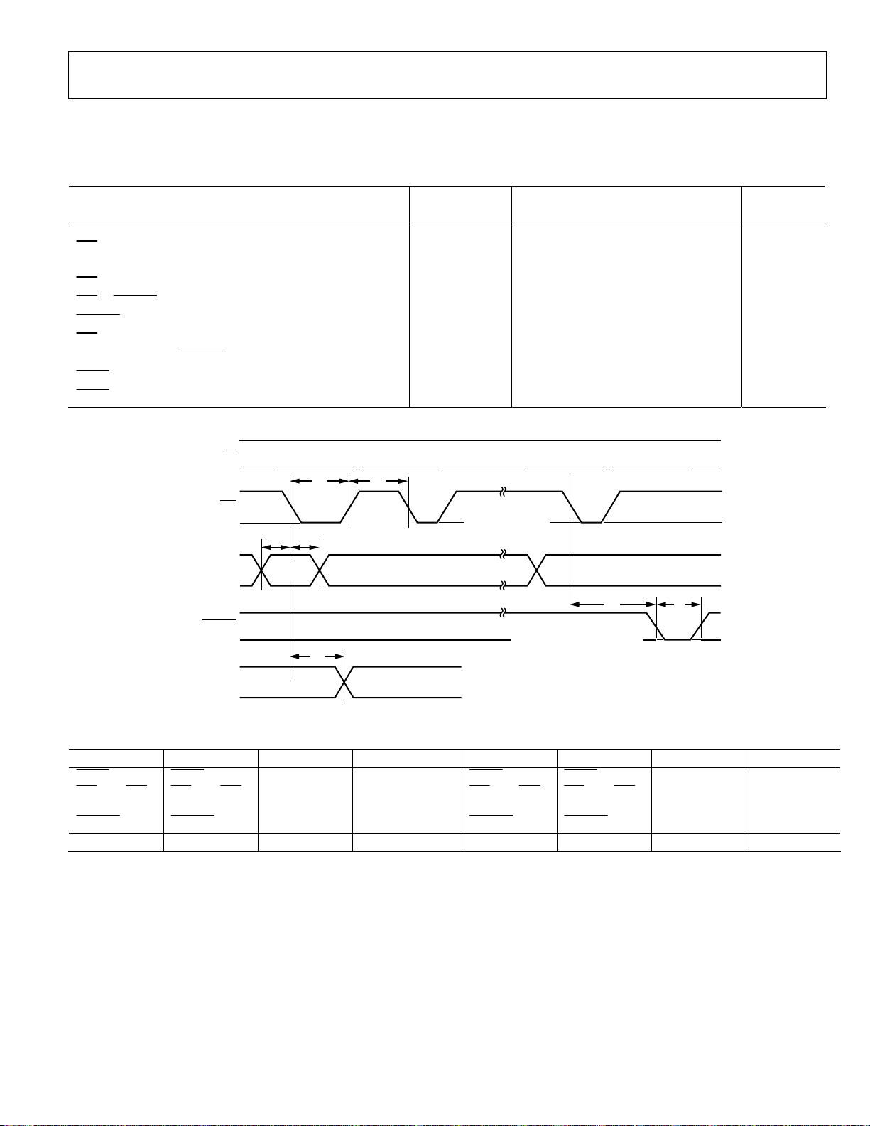
TIMING CHARACTERISTICS (SERIAL MODE)
Specifications subject to change without notice.
Table 2.
Limit
Parameter Symbol Min Typ Max Unit
Serial Data Setup Time t
CLK Pulse Width
Serial Data Hold Time t
CLK Pulse Separation
CLK to UPDATE Delay
UPDATE Pulse Width
CLK to DATA OUT Valid
Propagation Delay, UPDATE to Switch On or Off
RESET Pulse Width
RESET Time
1
WE
CLK
DATA IN
1 = LATCHED
UPDATE
0 = TRANSPARENT
DATA OUT
0
1
0
t1t
1
OUT31 (D5)
0
t
2
3
t
7
t
4
OUT30 (D4) OUT00 (D0)
Figure 2. Timing Diagram, Serial Mode
1
t
2
3
t
4
t
5
t
6
t
7
100 ns
60 ns
200 ns
LOAD DAT A INT O
SERIAL REGI STER
ON FALLING EDGE
40 ns
50 ns
50 ns
150 ns
10 ns
90 ns
120 ns
t
5
TRANSFER DATA F ROM SERIAL
REGISTER TO PARALLEL
LATCHES DURING LOW LEVEL
t
6
06365-002
Table 3. Logic Levels
VIH V
RESET,
SER/PAR, CLK,
DATA IN,
UPDATE
IL
RESET,
SER/PAR, CLK,
DATA IN,
UPDATE
V
OH
DATA OUT DATA OUT
2.0 V min 0.6 V max VDD − 0.3 V min D
1
See Figure 15.
V
OL
+ 0.5 V max 1 A max –1 A min −1 mA max 1 mA min
GND
Rev. A | Page 5 of 36
I
IH
RESET1,
SER/PAR, CLK,
DATA IN,
UPDATE
I
IL
RESET1,
SER/PAR, CLK,
DATA IN,
UPDATE
I
OH
DATA OUT DATA OUT
I
OL
Page 6
AD8117/AD8118
TIMING CHARACTERISTICS (PARALLEL MODE)
Specifications subject to change without notice.
Table 4.
Limit
Parameter Symbol Min Typ Max Unit
Parallel Data Setup Time t
WE Pulse Width
Parallel Data Hold Time t
WE Pulse Separation
WE to UPDATE Delay
UPDATE Pulse Width
Propagation Delay, UPDATE to Switch On or Off
RESET Pulse Width
RESET Time
WE
D0 TO D5
A0 TO A4
1 = LATCHED
0 = TRANSPARENT
UPDATE
t
1
0
t1t
1
0
2
3
t
4
Figure 3. Timing Diagram, Parallel Mode
1
t
2
3
t
4
t
5
t
6
100 ns
60 ns
200 ns
80 ns
110 ns
150 ns
90 ns
10 ns
90 ns
t
t
5
6
06365-003
Table 5. Logic Levels
VIH V
RESET,
SER/PAR, WE,
D0, D1, D2, D3,
D4, D5, A0, A1,
A2, A3, A4,
UPDATE
IL
RESET,
SER/PAR, WE,
D0, D1, D2, D3,
D4, D5, A0, A1,
A2, A3, A4,
UPDATE
V
OH
V
OL
DATA OUT DATA OUT
I
IH
RESET1,
SER/PAR, WE,
D0, D1, D2, D3,
D4, D5, A0, A1,
A2, A3, A4,
UPDATE
I
IL
RESET1,
SER/PAR, WE,
D0, D1, D2, D3,
D4, D5, A0, A1,
A2, A3, A4,
UPDATE
I
OH
I
OL
DATA OUT DATA OUT
2.0 V min 0.6 V max Disabled Disabled 1 µA max –1 µA min Disabled Disabled
1
See Figure 15.
Rev. A | Page 6 of 36
Page 7
AD8117/AD8118
ABSOLUTE MAXIMUM RATINGS
Table 6.
Parameter Rating
Analog Supply Voltage (V
Digital Supply Voltage (VDD – D
Ground Potential Difference
– D
(V
NEG
GND
)
Maximum Potential Difference
(V
– V
NEG
)
DD
Common-Mode Analog Input
POS
– V
) 6 V
NEG
) 6 V
GND
+0.5 V to −2.5 V
8 V
to V
V
NEG
POS
Voltage
Differential Analog Input Voltage ±2 V
Digital Input Voltage V
Output Voltage
DD
− 1 V) to (V
(V
POS
NEG
+ 1 V)
(Disabled Analog Output)
Output Short-Circuit Duration Momentary
Output Short-Circuit Current 80 mA
Storage Temperature −65°C to +125°C
Operating Temperature Range −40°C to +85°C
Lead Temperature
300°C
(Soldering 10 sec)
Junction Temperature 150°C
Stresses above those listed under Absolute Maximum Ratings
may cause permanent damage to the device. This is a stress
rating only; functional operation of the device at these or any
other conditions above those indicated in the operational
section of this specification is not implied. Exposure to absolute
maximum rating conditions for extended periods may affect
device reliability.
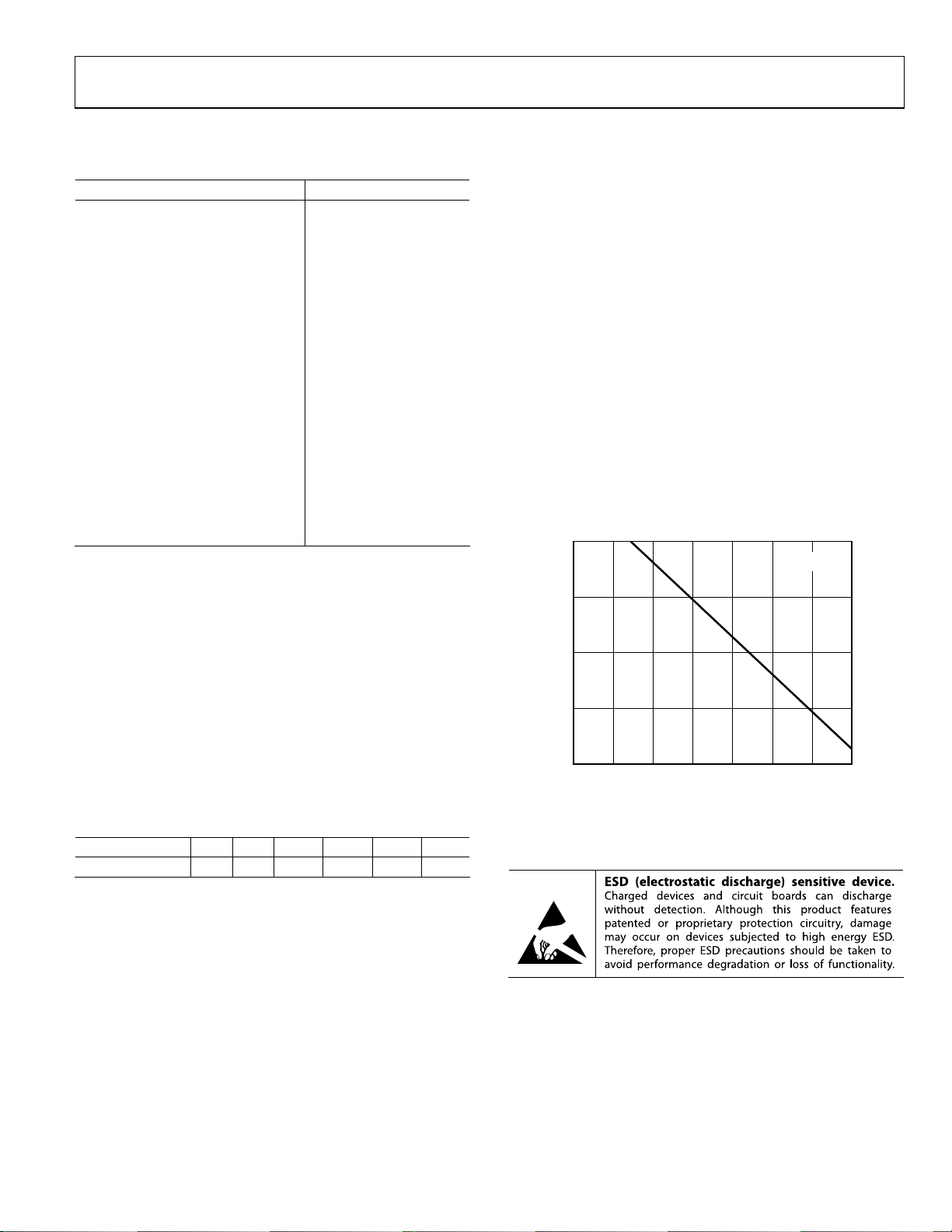
POWER DISSIPATION
The AD8117/AD8118 are operated with ±2.5 V or +5 V
supplies and can drive loads down to 100 , resulting in a large
range of possible power dissipations. For this reason, extra care
must be taken derating the operating conditions based on
ambient temperature.
Packaged in a 304-ball BGA, the AD8117/AD8118 junction-toambient thermal impedance (θ
reliability, the maximum allowed junction temperature of the
die should not exceed 150°C. Temporarily exceeding this limit
may cause a shift in parametric performance due to a change in
stresses exerted on the die by the package. Exceeding a junction
temperature of 175°C for an extended period can result in
device failure. The following curve shows the range of allowed
internal die power dissipations that meet these conditions over
the −40°C to +85°C ambient temperature range. When using
the table, do not include external load power in the maximum
power calculation, but do include load current dropped on the
die output transistors.
8
7
6
MAXIMUM POWER (W)
5
) is 14°C/W. For long-term
JA
TJ = 150°C
THERMAL RESISTANCE
θJA is specified for the worst-case conditions, that is, a device
soldered in a circuit board for surface-mount packages.
Table 7. Thermal Resistance
Package Type θ
304-Ball BGA 14 1 6.5 0.6 5.7 °C/W
θ
JA
θ
JC
ψ
JB
ψ
JT
Unit
JB
Rev. A | Page 7 of 36
4
25 35 45 55 65 75
15 85
Figure 4. Maximum Die Power Dissipation vs. Ambient Temperature
AMBIENT TEMPERATURE (°C)
ESD CAUTION
06365-004
Page 8
AD8117/AD8118
AA
A
A
PIN CONFIGURATION AND FUNCTION DESCRIPTIONS
23 22 21 20 19 18 17 16 15 14 13 12 11 10 9 8 7 6 5 4 3 2 1
VPOS
VPOS
VPOS
VPOS
VPOS
VPOS
A
VPOS
VPOS
VPOS
B
VPOS
VPOS
VPOS
C
VPOS
VPOS
IN16
D
VNEG
IN17
IP16
E
VNEG
IP17
IN18
F
VNEG
IN19
IP18
G
VNEG
IP19
IN20
H
VNEG
IN21
IP20
J
VNEG
IP21
IN22
K
VPOS
IN23
IP22
L
VPOS
IP23
IN24
M
VPOS
IN25
IP24
N
VNEG
IP25
IN26
P
VNEG
IN27
IP26
R
VNEG
IP27
IN28
T
VNEG
IN29
IP28
U
VNEG
IP29
IN30
V
VNEG
IN31
IP30
W
VPOS
IP31
VPOS
Y
VPOS
VPOS
VPOS
VPOS
VPOS
VPOS
B
VPOS
VPOS
VPOS
C
OP16
VPOS
VNEG
VOCM
VDD
DGND
RESET
WE
D5
D4
D3
D2
D1
D0
VDD
DGND
VOCM
VNEG
VPOS
VPOS
ON15
OP17
ON16
VNEG
VOCM
VOCM
VNEG
ON14
OP15
ON17
OP18
VNEG
VNEG
VNEG
VNEG
OP14
ON13
OP19
ON18
VNEG
VNEG
VNEG
VNEG
ON12
OP13
OP21
ON19
OP20
VNEG
VNEG
ON21 OP23 ON23 OP25 ON25 OP27 ON27 OP29 ON29
ON20
OP22 ON22 OP24 ON24 OP26 ON26 OP28 ON28 OP30
VNEG
VNEG VPO S VPOS VPOS VNEG VNEG VNEG VNEG VNEG
VNEG
VNEG VPO S VPOS VPOS VNEG VNEG VNEG VNEG VNEG
AD8117/AD8118
BOTTOM VIEW
(Not to Scale)
VNEG
VNEG
VNEG
OP12
ON11
VNEG VPO S VPOS VPOS VNEG VNEG VNEG VNEG VNEG
VNEG
VNEG VPO S VPOS VPOS VNEG VNEG VNEG VNEG VNEG
ON10
OP10 ON8 OP8 O N6 O P6 ON4 OP4 ON2 OP2
OP11 ON9 OP9 ON7 OP7 ON5 OP5 ON3 OP3 ON1
OP31
ON30
VNEG
VOCM
VOCM
VNEG
ON0
OP1
ON31
VPOS
VPOS
VNEG
VOCM
VDD
DGND
DATA
OUT
CLK
DATA
IN
SER/
PAR
A4
A3
A2
A1
A0
VDD
DGND
VOCM
VNEG
VPOS
OP0
VPOS
VPOS
VPOS
VPOS
VPOS
VNEG
VNEG
VNEG
VNEG
VNEG
VNEG
VPOS
VPOS
VPOS
VNEG
VNEG
VNEG
VNEG
VNEG
VNEG
VPOS
VPOS
VPOS
VPOS
VPOS
VPOS
IP0
IN0
IP2
IN2
IP4
IN4
IP6
IN6
IP8
IN8
IP10
IN10
IP12
IN12
IP14
IN14
VPOS
VPOS
VPOS
VPOS
VPOS
VPOS
VPOS
IP1
IN1
IP3
IN3
IP5
IN5
IP7
IN7
IP9
IN9
IP11
IN11
IP13
IN13
IP15
IN15
VPOS
VPOS
VPOS
A
B
C
D
E
F
G
H
J
K
L
M
N
P
R
T
U
V
W
Y
AA
AB
AC
23 22 21 20 19 18 17 16 15 14 13 12 11 10 9 8 7 6 5 4 3 2 1
Figure 5. Package Bottom View
Rev. A | Page 8 of 36
6365-005
Page 9
AD8117/AD8118
VPOS
VPOS
VPOS
ON31
AA
AB
AC
VPOS
VPOS
VNEG
VOCM
VDD
DGND
DATA
OUT
CLK
DATA
IN
SER/
PAR
A4
A3
A2
A1
A0
VDD
DGND
VOCM
VNEG
VPOS
OP0
VPOS
OP31
ON30
VNEG
VOCM
VOCM
VNEG
ON0
OP1
AD8117/AD8118
TOP VIEW
(Not to Scale)
A
VPOS
VPOS
VPOS
IP0
IN0
IP2
IN2
IP4
IN4
IP6
IN6
IP8
IN8
IP10
IN10
IP12
IN12
IP14
IN14
VPOS
VPOS
VPOS
VPOS
VPOS
VPOS
VPOS
VNEG
VNEG
VNEG
VNEG
VNEG
VNEG
VPOS
VPOS
VPOS
VNEG
VNEG
VNEG
VNEG
VNEG
VNEG
VPOS
VPOS
VPOS
VPOS
B
VPOS
C
VPOS
D
IP1
E
IN1
F
IP3
G
IN3
H
IP5
J
IN5
K
IP7
L
IN7
M
IP9
N
IN9
P
IP11
R
IN11
T
IP13
U
IN13
V
IP15
W
IN15
Y
VPOS
VPOS
VPOS
OP21
ON19
OP19
ON17
OP18
VNEG
VNEG
VNEG
VNEG
OP14
ON13
OP17
ON16
VNEG
VOCM
VOCM
VNEG
ON14
OP15
ON21OP23ON23OP25ON25OP27ON27OP29ON29
ON20
OP20
VNEG
VNEG
VNEG
VNEG
OP12
ON11
ON18
VNEG
VNEG
VNEG
VNEG
ON12
OP13
OP22ON22OP24ON24OP26ON26OP28ON28OP30
VNEG
VNEGVPOSVPOSVPOSVNEGVNEGVNEGVNEGVNEG
VNEG
VNEGVPO SVPOSVPOSVNEGVNEGVNEGVNEGVNEG
VNEG
VNEGVPO SVPOSVPOSVNEGVNEGVNEGVNEGVNEG
VNEG
VNEGVPO SVPOSVPOSVNEGVNEGVNEGVNEGVNEG
ON10
OP10ON8OP8ON6OP6ON4OP4ON2OP2
OP11ON9OP9ON7OP7ON5OP5ON3OP3ON1
VPOS
OP16
VPOS
VNEG
VOCM
VDD
DGND
RESET
WE
D5
D4
D3
D2
D1
D0
VDD
DGND
VOCM
VNEG
VPOS
VPOS
ON15
23 22 212019181716151413121110987654321
VPOS
VPOS
VPOS
VPOS
VNEG
VNEG
VNEG
VNEG
VNEG
VNEG
VPOS
VPOS
VPOS
VNEG
VNEG
VNEG
VNEG
VNEG
VNEG
VPOS
VPOS
VPOS
VPOS
VPOS
VPOS
VPOS
VPOS
IN17
IP17
IN19
IP19
IN21
IP21
IN23
IP23
IN25
IP25
IN27
IP27
IN29
IP29
IN31
IP31
VPOS
VPOS
VPOS
VPOS
VPOS
VPOS
IN16
IP16
IN18
IP18
IN20
IP20
IN22
IP22
IN24
IP24
IN26
IP26
IN28
IP28
IN30
IP30
VPOS
VPOS
VPOS
VPOS
A
B
C
D
E
F
G
H
J
K
L
M
N
P
R
T
U
V
W
Y
AA
AB
AC
Figure 6. Package Top View
Table 8. Ball Grid Description
Ball No. Mnemonic Description
A1 VPOS Analog Positive Power Supply.
A2 VPOS Analog Positive Power Supply.
A3 VPOS Analog Positive Power Supply.
A4 ON31 Output Number 31, Negative Phase.
A5 OP31 Output Number 31, Positive Phase.
A6 ON29 Output Number 29, Negative Phase.
A7 OP29 Output Number 29, Positive Phase.
A8 ON27 Output Number 27, Negative Phase.
A9 OP27 Output Number 27, Positive Phase.
A10 ON25 Output Number 25, Negative Phase.
A11 OP25 Output Number 25, Positive Phase.
A12 ON23 Output Number 23, Negative Phase.
A13 OP23 Output Number 23, Positive Phase.
A14 ON21 Output Number 21, Negative Phase.
Ball No. Mnemonic Description
A15 OP21 Output Number 21, Positive Phase.
A16 ON19 Output Number 19, Negative Phase.
A17 OP19 Output Number 19, Positive Phase.
A18 ON17 Output Number 17, Negative Phase.
A19 OP17 Output Number 17, Positive Phase.
A20 VPOS Analog Positive Power Supply.
A21 VPOS Analog Positive Power Supply.
A22 VPOS Analog Positive Power Supply.
A23 VPOS Analog Positive Power Supply.
B1 VPOS Analog Positive Power Supply.
B2 VPOS Analog Positive Power Supply.
B3 VPOS Analog Positive Power Supply.
B4 VPOS Analog Positive Power Supply.
B5 ON30 Output Number 30, Negative Phase.
Rev. A | Page 9 of 36
2322212019181716151413121110987654321
6365-006
Page 10
AD8117/AD8118
Ball No. Mnemonic Description
B6 OP30 Output Number 30, Positive Phase.
B7 ON28 Output Number 28, Negative Phase.
B8 OP28 Output Number 28, Positive Phase.
B9 ON26 Output Number 26, Negative Phase.
B10 OP26 Output Number 26, Positive Phase.
B11 ON24 Output Number 24, Negative Phase.
B12 OP24 Output Number 24, Positive Phase.
B13 ON22 Output Number 22, Negative Phase.
B14 OP22 Output Number 22, Positive Phase.
B15 ON20 Output Number 20, Negative Phase.
B16 OP20 Output Number 20, Positive Phase.
B17 ON18 Output Number 18, Negative Phase.
B18 OP18 Output Number 18, Positive Phase.
B19 ON16 Output Number 16, Negative Phase.
B20 OP16 Output Number 16, Positive Phase.
B21 VPOS Analog Positive Power Supply.
B22 VPOS Analog Positive Power Supply.
B23 VPOS Analog Positive Power Supply.
C1 VPOS Analog Positive Power Supply.
C2 VPOS Analog Positive Power Supply.
C3 VPOS Analog Positive Power Supply.
C4 VPOS Analog Positive Power Supply.
C5 VNEG Analog Negative Power Supply.
C6 VNEG Analog Negative Power Supply.
C7 VNEG Analog Negative Power Supply.
C8 VNEG Analog Negative Power Supply.
C9 VNEG Analog Negative Power Supply.
C10 VNEG Analog Negative Power Supply.
C11 VPOS Analog Positive Power Supply.
C12 VPOS Analog Positive Power Supply.
C13 VPOS Analog Positive Power Supply.
C14 VNEG Analog Negative Power Supply.
C15 VNEG Analog Negative Power Supply.
C16 VNEG Analog Negative Power Supply.
C17 VNEG Analog Negative Power Supply.
C18 VNEG Analog Negative Power Supply.
C19 VNEG Analog Negative Power Supply.
C20 VPOS Analog Positive Power Supply.
C21 VPOS Analog Positive Power Supply.
C22 VPOS Analog Positive Power Supply.
C23 VPOS Analog Positive Power Supply.
D1 VPOS Analog Positive Power Supply.
D2 IP0 Input Number 0, Positive Phase.
D3 VPOS Analog Positive Power Supply.
D4 VNEG Analog Negative Power Supply.
D5 VOCM
D6 VNEG Analog Negative Power Supply.
D7 VNEG Analog Negative Power Supply.
D8 VNEG Analog Negative Power Supply.
D9 VNEG Analog Negative Power Supply.
D10 VNEG Analog Negative Power Supply.
D11 VPOS Analog Positive Power Supply.
Output Common-Mode Reference
Supply.
Ball No. Mnemonic Description
D12 VPOS Analog Positive Power Supply.
D13 VPOS Analog Positive Power Supply.
D14 VNEG Analog Negative Power Supply.
D15 VNEG Analog Negative Power Supply.
D16 VNEG Analog Negative Power Supply.
D17 VNEG Analog Negative Power Supply.
D18 VNEG Analog Negative Power Supply.
D19 VOCM
D20 VNEG Analog Negative Power Supply.
D21 VPOS Analog Positive Power Supply.
D22 VPOS Analog Positive Power Supply.
D23 IN16 Input Number 16, Negative Phase.
E1 IP1 Input Number 1, Positive Phase.
E2 IN0 Input Number 0, Negative Phase.
E3 VNEG Analog Negative Power Supply.
E4 VOCM
E20 VOCM
E21 VNEG Analog Negative Power Supply.
E22 IN17 Input Number 17, Negative Phase.
E23 IP16 Input Number 16, Positive Phase.
F1 IN1 Input Number 1, Negative Phase.
F2 IP2 Input Number 2, Positive Phase.
F3 VNEG Analog Negative Power Supply.
F4 VDD Logic Positive Power Supply.
F20 VDD Logic Positive Power Supply.
F21 VNEG Analog Negative Power Supply.
F22 IP17 Input Number 17, Positive Phase.
F23 IN18 Input Number 18, Negative Phase.
G1 IP3 Input Number 3, Positive Phase.
G2 IN2 Input Number 2, Negative Phase.
G3 VNEG Analog Negative Power Supply.
G4 DGND Logic Negative Power Supply.
G20 DGND Logic Negative Power Supply.
G21 VNEG Analog Negative Power Supply.
G22 IN19 Input Number 19, Negative Phase.
G23 IP18 Input Number 18, Positive Phase.
H1 IN3 Input Number 3, Negative Phase.
H2 IP4 Input Number 4, Positive Phase.
H3 VNEG Analog Negative Power Supply.
H4 DATA OUT Control Pin: Serial Data Out.
H20
H21 VNEG Analog Negative Power Supply.
H22 IP19 Input Number 19, Positive Phase.
H23 IN20 Input Number 20, Negative Phase.
J1 IP5 Input Number 5, Positive Phase.
J2 IN4 Input Number 4, Negative Phase.
J3 VNEG Analog Negative Power Supply.
J4
J20
RESET
CLK
UPDATE
Output Common-Mode Reference
Supply.
Output Common-Mode Reference
Supply.
Output Common-Mode Reference
Supply.
Control Pin: Second Rank Data Reset.
Control Pin: Serial Data Clock.
Control Pin: Second Rank Write Strobe.
Rev. A | Page 10 of 36
Page 11
AD8117/AD8118
Ball No. Mnemonic Description
J21 VNEG Analog Negative Power Supply.
J22 IN21 Input Number 21, Negative Phase.
J23 IP20 Input Number 20, Positive Phase.
K1 IN5 Input Number 5, Negative Phase.
K2 IP6 Input Number 6, Positive Phase.
K3 VNEG Analog Negative Power Supply.
K4 DATA IN Control Pin: Serial Data In.
K20
K21 VNEG Analog Negative Power Supply.
K22 IP21 Input Number 21, Positive Phase.
K23 IN22 Input Number 22, Negative Phase.
L1 IP7 Input Number 7, Positive Phase.
L2 IN6 Input Number 6, Negative Phase.
L3 VPOS Analog Positive Power Supply.
L4
L20 D5 Control Pin: Input Address Bit 5.
L21 VPOS Analog Positive Power Supply.
L22 IN23 Input Number 23, Negative Phase.
L23 IP22 Input Number 22, Positive Phase.
M1 IN7 Input Number 7, Negative Phase.
M2 IP8 Input Number 8, Positive Phase.
M3 VPOS Analog Positive Power Supply.
M4 A4 Control Pin: Output Address Bit 4.
M20 D4 Control Pin: Input Address Bit 4.
M21 VPOS Analog Positive Power Supply.
M22 IP23 Input Number 23, Positive Phase.
M23 IN24 Input Number 24, Negative Phase.
N1 IP9 Input Number 9, Positive Phase.
N2 IN8 Input Number 8, Negative Phase.
N3 VPOS Analog Positive Power Supply.
N4 A3 Control Pin: Output Address Bit 3.
N20 D3 Control Pin: Input Address Bit 3.
N21 VPOS Analog Positive Power Supply.
N22 IN25 Input Number 25, Negative Phase.
N23 IP24 Input Number 24, Positive Phase.
P1 IN9 Input Number 9, Negative Phase.
P2 IP10 Input Number 10, Positive Phase.
P3 VNEG Analog Negative Power Supply.
P4 A2 Control Pin: Output Address Bit 2.
P20 D2 Control Pin: Input Address Bit 2.
P21 VNEG Analog Negative Power Supply.
P22 IP25 Input Number 25, Positive Phase.
P23 IN26 Input Number 26, Negative Phase.
R1 IP11 Input Number 11, Positive Phase.
R2 IN10 Input Number 10, Negative Phase.
R3 VNEG Analog Negative Power Supply.
R4 A1 Control Pin: Output Address Bit 1.
R20 D1 Control Pin: Input Address Bit 1.
R21 VNEG Analog Negative Power Supply.
R22 IN27 Input Number 27, Negative Phase.
R23 IP26 Input Number 26, Positive Phase.
T1 IN11 Input Number 11, Negative Phase.
WE
SER/PAR
Control Pin: First Rank Write Strobe.
Control Pin: Serial/Parallel Mode Select.
Ball No. Mnemonic Description
T2 IP12 Input Number 12, Positive Phase.
T3 VNEG Analog Negative Power Supply.
T4 A0 Control Pin: Output Address Bit 0.
T20 D0 Control Pin: Input Address Bit 0.
T21 VNEG Analog Negative Power Supply.
T22 IP27 Input Number 27, Positive Phase.
T23 IN28 Input Number 28, Negative Phase.
U1 IP13 Input Number 13, Positive Phase.
U2 IN12 Input Number 12, Negative Phase.
U3 VNEG Analog Negative Power Supply.
U4 VDD Logic Positive Power Supply.
U20 VDD Logic Positive Power Supply.
U21 VNEG Analog Negative Power Supply.
U22 IN29 Input Number 29, Negative Phase.
U23 IP28 Input Number 28, Positive Phase.
V1 IN13 Input Number 13, Negative Phase.
V2 IP14 Input Number 14, Positive Phase.
V3 VNEG Analog Negative Power Supply.
V4 DGND Logic Negative Power Supply.
V20 DGND Logic Negative Power Supply.
V21 VNEG Analog Negative Power Supply.
V22 IP29 Input Number 29, Positive Phase.
V23 IN30 Input Number 30, Negative Phase.
W1 IP15 Input Number 15, Positive Phase.
W2 IN14 Input Number 14, Negative Phase.
W3 VNEG Analog Negative Power Supply.
W4 VOCM
W20 VOCM
W21 VNEG Analog Negative Power Supply.
W22 IN31 Input Number 31, Negative Phase.
W23 IP30 Input Number 30, Positive Phase.
Y1 IN15 Input Number 15, Negative Phase.
Y2 VPOS Analog Positive Power Supply.
Y3 VPOS Analog Positive Power Supply.
Y4 VNEG Analog Negative Power Supply.
Y5 VOCM
Y6 VNEG Analog Negative Power Supply.
Y7 VNEG Analog Negative Power Supply.
Y8 VNEG Analog Negative Power Supply.
Y9 VNEG Analog Negative Power Supply.
Y10 VNEG Analog Negative Power Supply.
Y11 VPOS Analog Positive Power Supply.
Y12 VPOS Analog Positive Power Supply.
Y13 VPOS Analog Positive Power Supply.
Y14 VNEG Analog Negative Power Supply.
Y15 VNEG Analog Negative Power Supply.
Y16 VNEG Analog Negative Power Supply.
Y17 VNEG Analog Negative Power Supply.
Y18 VNEG Analog Negative Power Supply.
Output Common-Mode Reference
Supply.
Output Common-Mode Reference
Supply.
Output Common-Mode Reference
Supply.
Rev. A | Page 11 of 36
Page 12

AD8117/AD8118
Ball No. Mnemonic Description
Y19 VOCM
Y20 VNEG Analog Negative Power Supply.
Y21 VPOS Analog Positive Power Supply.
Y22 IP31 Input Number 31, Positive Phase.
Y23 VPOS Analog Positive Power Supply.
AA1 VPOS Analog Positive Power Supply.
AA2 VPOS Analog Positive Power Supply.
AA3 VPOS Analog Positive Power Supply.
AA4 VPOS Analog Positive Power Supply.
AA5 VNEG Analog Negative Power Supply.
AA6 VNEG Analog Negative Power Supply.
AA7 VNEG Analog Negative Power Supply.
AA8 VNEG Analog Negative Power Supply.
AA9 VNEG Analog Negative Power Supply.
AA10 VNEG Analog Negative Power Supply.
AA11 VPOS Analog Positive Power Supply.
AA12 VPOS Analog Positive Power Supply.
AA13 VPOS Analog Positive Power Supply.
AA14 VNEG Analog Negative Power Supply.
AA15 VNEG Analog Negative Power Supply.
AA16 VNEG Analog Negative Power Supply.
AA17 VNEG Analog Negative Power Supply.
AA18 VNEG Analog Negative Power Supply.
AA19 VNEG Analog Negative Power Supply.
AA20 VPOS Analog Positive Power Supply.
AA21 VPOS Analog Positive Power Supply.
AA22 VPOS Analog Positive Power Supply.
AA23 VPOS Analog Positive Power Supply.
AB1 VPOS Analog Positive Power Supply.
AB2 VPOS Analog Positive Power Supply.
AB3 VPOS Analog Positive Power Supply.
AB4 OP0 Output Number 0, Positive Phase.
AB5 ON0 Output Number 0, Negative Phase.
AB6 OP2 Output Number 2, Positive Phase.
AB7 ON2 Output Number 2, Negative Phase.
AB8 OP4 Output Number 4, Positive Phase.
AB9 ON4 Output Number 4, Negative Phase.
Output Common-Mode Reference
Supply.
Ball No. Mnemonic Description
AB10 OP6 Output Number 6, Positive Phase.
AB11 ON6 Output Number 6, Negative Phase.
AB12 OP8 Output Number 8, Positive Phase.
AB13 ON8 Output Number 8, Negative Phase.
AB14 OP10 Output Number 10, Positive Phase.
AB15 ON10 Output Number 10, Negative Phase.
AB16 OP12 Output Number 12, Positive Phase.
AB17 ON12 Output Number 12, Negative Phase.
AB18 OP14 Output Number 14, Positive Phase.
AB19 ON14 Output Number 14, Negative Phase.
AB20 VPOS Analog Positive Power Supply.
AB21 VPOS Analog Positive Power Supply.
AB22 VPOS Analog Positive Power Supply.
AB23 VPOS Analog Positive Power Supply.
AC1 VPOS Analog Positive Power Supply.
AC2 VPOS Analog Positive Power Supply.
AC3 VPOS Analog Positive Power Supply.
AC4 VPOS Analog Positive Power Supply.
AC5 OP1 Output Number 1, Positive Phase.
AC6 ON1 Output Number 1, Negative Phase.
AC7 OP3 Output Number 3, Positive Phase.
AC8 ON3 Output Number 3, Negative Phase.
AC9 OP5 Output Number 5, Positive Phase.
AC10 ON5 Output Number 5, Negative Phase.
AC11 OP7 Output Number 7, Positive Phase.
AC12 ON7 Output Number 7, Negative Phase.
AC13 OP9 Output Number 9, Positive Phase.
AC14 ON9 Output Number 9, Negative Phase.
AC15 OP11 Output Number 11, Positive Phase.
AC16 ON11 Output Number 11, Negative Phase.
AC17 OP13 Output Number 13, Positive Phase.
AC18 ON13 Output Number 13, Negative Phase.
AC19 OP15 Output Number 15, Positive Phase.
AC20 ON15 Output Number 15, Negative Phase.
AC21 VPOS Analog Positive Power Supply.
AC22 VPOS Analog Positive Power Supply.
AC23 VPOS Analog Positive Power Supply.
Rev. A | Page 12 of 36
Page 13

AD8117/AD8118
TRUTH TABLE AND LOGIC DIAGRAM
Table 9. Operation Truth Table
WE UPDATE CLK
INPUT
X X X X X 0 X
0 X X D0…D5
DATA
1 X
Data
2
i
0 X X D0…D5
A0…A4
1 0 X X
1 X X X X 1 1 No change in logic.
1
D0…D5: data bits.
2
Datai: serial data.
3
A0…A4: address bits.
1
1
3
DATA
OUTPUT
NA in
parallel
mode
Data
i-192
NA in
parallel
mode
NA in
parallel
mode
/PAR
RESET
SER
1 0
1 0
1 1
1 X
Operation/Comment
Asynchronous reset. All outputs are
disabled. Remainder of logic in 192-bit shift
register is unchanged.
Broadcast. The data on parallel lines D0 to
D5 are loaded into all 32 output address
locations of the 192-bit shift register.
Serial mode. The data on the serial DATA IN
line is loaded into the serial register. The first
bit clocked into the serial register appears
at DATA OUT 192 clock cycles later.
Parallel programming mode. The data on
parallel lines D0 to D5 are loaded into the
shift register location addressed by A0 to A4.
Switch matrix update. Data in the 192-bit
shift register transfers into the parallel
latches that control the switch array.
Rev. A | Page 13 of 36
Page 14

AD8117/AD8118
DATA OUT
(SERIAL)
D
Q
D
CLK
Q
S
D1
D0
DQ
CLK
Q
S
D1
D0
DQ
CLK
Q
S
D1
D0
DQ
CLK
Q
S
D1
D0
DQ
CLK
Q
S
D1
D0
DQ
CLK
Q
S
D1
D0
DQ
CLK
Q
S
D1
D0
DQ
CLK
Q
S
D1
D0
DQ
CLK
Q
S
D1
D0
DQ
CLK
Q
S
D1
D0
Q
D
CLK
Q
S
D1
D0
DQ
CLK
Q
S
D1
D0
Q
D
CLK
Q
S
D1
D0
DQ
CLK
Q
S
D1
D0
ENA
D
ENA
D
ENA
D
ENA
D
ENA
D
ENA
D
ENA
D
ENA
D
ENA
D
ENA
D
ENA
D
ENA
D
ENA
D
ENA
Q
EN
OUT31
CLR
Q
B4
OUT31
CLR
Q
B3
OUT31
CLR
Q
B2
OUT31
CLR
Q
B1
OUT31
CLR
Q
B0
OUT31
CLR
Q
EN
OUT30
CLR
Q
B0
OUT1
CLR
Q
EN
OUT0
CLR
Q
B4
OUT0
CLR
Q
B3
OUT0
CLR
Q
B2
OUT0
CLR
Q
B1
OUT0
CLR
Q
B0
OUT0
CLR
06365-007
32
OUTPUT ENABLE
DECODE
1024
SWITCH MATRIX
D0D1D2D3D4
PARALLEL DATA
D5
RESET
UPDATE
WE
SER/PAR
(OUTPUT ENABLE)
DATA IN
CLK
(SERIAL)
OUT0 EN
OUT1 EN
OUT2 EN
OUT3 EN
OUT4 EN
OUT5 EN
OUT6 EN
OUT7 EN
OUT8 EN
OUT9 EN
OUT10 EN
OUT11 EN
OUT12 EN
OUT13 EN
OUT14 EN
OUT15 EN
OUT16 EN
OUT17 EN
OUT18 EN
OUT19 EN
OUT20 EN
OUT21 EN
OUT22 EN
OUT23 EN
OUT24 EN
OUT25 EN
OUT26 EN
OUT27 EN
OUT28 EN
OUT29 EN
5 TO 32 DECODER
ADDRESS
OUTPUT
A4A3A2A1A0
OUT30 EN
OUT31 EN
Figure 7. Logic Diagram
Rev. A | Page 14 of 36
Page 15

AD8117/AD8118
Ω
n
n
V
V
I/O SCHEMATICS
OPn, ONn
06365-008
Figure 8. AD8117/AD8118 Enabled Output
(see also ESD Protection Map,
0.4pF 30kΩ
Figure 18)
OPn
3.4pF
3.4pF
ONn
Figure 9. AD8117/AD8118 Disabled Output
2500Ω
2500Ω
Figure 18)
2538Ω
2538Ω
(see also ESD Protection Map,
IPn
INn
1.3pF
0.3pF
1.3pF
IP
INn
0.3pF
1.3pF
1.3pF
2500Ω
2500Ω
6365-011
Figure 12. AD8117/AD8118 Receiver Simplified Equivalent Circuit When
Driving Differentially
IP
3.33kΩ AD8117 G = +1
1.6pF
3.76kΩ AD8118 G = +2
INn
06365-009
6365-012
Figure 13. AD8117/AD8118 Receiver Simplified Equivalent Circuit When
Driving Single-Ended
OCM
VNEG
6365-013
06365-010
Figure 10. AD8117 Receiver (see also ESD Protection Map,
IPn
INn
2500
1.3pF
0.3pF
1.3pF
2500Ω 5075Ω
5075Ω
Figure 11. AD8118 Receiver (see also ESD Protection Map,
Figure 18)
06365-068
Figure 18)
Rev. A | Page 15 of 36
Figure 14. VOCM Input (see also ESD Protection Map,
DD
25kΩ
RESET
1kΩ
DGND
6365-014
Figure 15. Reset Input (see also ESD Protection Map,
Figure 18)
Figure 18)
Page 16

AD8117/AD8118
V
V
V
CLK, SER/PAR, WE,
UPDATE, DATA IN,
A[4:0], D[5:0]
1kΩ
Figure 16. Logic Input (see also ESD Protection Map,
DD
DATA OUT
DGND
Figure 17. Logic Output (see also ESD Protection Map,
DGND
6365-016
6365-015
Figure 18)
Figure 18)
IPn, INn,
OPn, ONn,
VOCM
POS
VNEG
Figure 18. ESD Protection Map
DD
DGND
CLK, RESET,
SER/PAR, WE,
UPDATE,
DATA IN,
DATA OUT,
A[4:0], D[5:0]
06365-017
Rev. A | Page 16 of 36
Page 17

AD8117/AD8118
TYPICAL PERFORMANCE CHARACTERISTICS
VS = ±2.5 V at TA = 25°C, R
10
8
6
4
2
0
GAIN (dB)
–2
–4
–6
–8
–10
1
Figure 19. AD8117, AD8118 Small Signal Frequency Response, 200 mV p-p
= 200 Ω, V
L, diff
10
FREQUENCY (MHz )
= 0 V, differential I/O mode, unless otherwise noted.
OCM
400
100
AD8118
AD8117
1000
6365-018
350
300
250
200
COUNT
150
100
50
0
540 700
FREQUENCY (MHz)
680660640620600580560
Figure 22. AD8117 −3 dB Bandwidth Histogram,
One Device, All 1024 Channels
06365-021
10
8
6
4
2
0
GAIN (dB)
–2
–4
–6
–8
–10
1
10
FREQUENCY (MHz)
100
AD8118
AD8117
1000
06365-019
Figure 20. AD8117, AD8118 Large Signal Frequency Response, 2 V p-p
10
8
6
4
2
0
–2
–4
NORMALIZE D GAIN (dB)
–6
–8
–10
01
FREQUENCY (MHz)
10pF
5pF
2pF
0pF
10010
000
06365-020
Figure 21. AD8117 Small Signal Frequency Response with Capacitive Loads,
200 mV p-p
0
–1
–2
NORMALIZE D BANDWIDTH ERROR ( %)
–3
NUMBER OF ENABLED CHANNELS
2624222012864218161410 3028
Figure 23. AD8117 Bandwidth Error vs. Enabled Channels
0
–10
–20
–30
–40
CMR (dB)
–50
–60
–70
300k 1M 10M 100M 1G 2G
FREQUENCY (Hz)
DIFFERENTIAL OUT
Figure 24. AD8117, AD8118 Common-Mode Rejection
32
06365-022
06365-023
Rev. A | Page 17 of 36
Page 18

AD8117/AD8118
–
15
–25
–35
V
–45
–55
PSR (dB)
–65
–75
–85
POS
V
NEG
AGGRESSOR
AGGRESSORDIFFERENTIAL OUT
V
AGGRESSOR
OCM
0
–20
–40
–60
CROSSTALK (dB)
–80
DIFFERENTIAL IN/O UT
–95
0.1 1000
FREQUENCY (MHz )
100101
Figure 25. AD8117 Power Supply Rejection
10
SINGLE-E NDED OUT
5
0
–5
–10
–15
–20
V
PSR (dB)
NEG
–25
–30
–35
–40
–45
–50
0.1 1000
V
OCM
AGGRESSOR
AGGRESSOR
V
AGGRESSOR
POS
FREQUENCY (MHz)
100101
Figure 26. AD8117 Power Supply Rejection, Single-Ended
180
160
140
120
100
80
60
40
NOISE SPECTRAL DENSITY (nV/ Hz)
20
0
1k 10k 100k 1M
AD8118
AD8117
FREQUENCY (Hz)
DIFFERENTIAL OUT
Figure 27. AD8117, AD8118 Noise Spectral Density, RTO
–100
300k 1M 10M 100M 1G
06365-024
FREQUENCY (Hz)
06365-027
Figure 28. AD8117 Crosstalk, One Adjacent Channel
0
–20
–40
–60
CROSSTALK (d B)
–80
–100
300k 1M 10M 100M 1G
06365-025
FREQUENCY (Hz)
DIFFERENTIAL IN/O UT
6365-070
Figure 29. AD8118 Crosstalk, One Adjacent Channel
0
–20
–40
–60
CROSSTALK (dB)
–80
–100
300k 1M 10M 100M 1G
06365-026
FREQUENCY (Hz)
SINGLE-E NDED IN/OUT
06365-028
Figure 30. AD8117 Crosstalk, One Adjacent Channel, Single-Ended
Rev. A | Page 18 of 36
Page 19

AD8117/AD8118
0
–20
–40
–60
CROSSTALK (dB)
–80
–100
300k 1M 10M 100M 1G
FREQUENCY (Hz)
SINGLE-ENDED IN/OUT
Figure 31. AD8118 Crosstalk, One Adjacent Channel, Single-Ended
0
–20
–40
DIFFERENTIAL IN/O UT
0
–20
–40
–60
CROSSTALK (dB)
–80
–100
300k 1M 10M 100M 1G
06365-071
FREQUENCY (Hz)
SINGLE-E NDED IN/OUT
06365-030
Figure 34. AD8117 Crosstalk, All Hostile, Single-Ended
0
–20
–40
SINGLE-ENDED IN/OUT
–60
CROSSTALK (dB)
–80
–100
300k 1M 10M 100M 1G
FREQUENCY (Hz)
Figure 32. AD8117 Crosstalk, All Hostile
0
–20
–40
–60
CROSSTALK (d B)
–80
–100
300k 1M 10M 100M 1G
FREQUENCY (Hz)
DIFFERENTIAL IN/OUT
Figure 33. AD8118 Crosstalk, All Hostile
–60
CROSSTALK (dB)
–80
–100
300k 1M 10M 100M 1G
06365-029
FREQUENCY (Hz)
06365-073
Figure 35. AD8118 Crosstalk, All Hostile, Single-Ended
0
–20
–40
–60
FEEDTHROUG H (dB)
–80
–100
300k 1M 10M 100M 1G 2G
6365-072
FREQUENCY (Hz)
DIFFERENTIAL IN/O UT
06365-031
Figure 36. AD8117 Crosstalk, Off Isolation
Rev. A | Page 19 of 36
Page 20

AD8117/AD8118
0
–20
–40
–60
FEEDTHROUG H (dB)
–80
–100
300k 1M 10M 100M 1G 2G
FREQUENCY (Hz)
SINGLE-E NDED IN/OUT
Figure 37. AD8117 Crosstalk, Off Isolation, Single-Ended
6k
AD8118
5k
AD8117
4k
3k
DIFFERENTIAL IN
06365-032
30k
25k
20k
15k
10k
OUTPUT IMPEDANCE (Ω)
5k
0
100k 1M 10M 100M 1G
FREQUENCY (Hz)
DIFFERENTIAL OUT
Figure 40. AD8117, AD8118 Output Impedance, Disabled
1000
100
10
06365-035
2k
INPUT IMP EDANCE (Ω)
1k
0
300k 1M 10M 100M 1G
FREQUENCY (Hz)
Figure 38. AD8117, AD8118 Input Impedance
4500
4000
3500
3000
2500
2000
1500
INPUT IMPE DANCE (Ω)
1000
500
0
300k 1M 10M 100M 1G
AD8118
AD8117
FREQUENCY (Hz)
SINGLE-E NDED IN
Figure 39. AD8117, AD8118 Input Impedance, Single-Ended
OUTPUT IMPEDANCE (Ω)
1
0.1
100k 1G
06365-033
10M 100M1M
FREQUENCY (Hz)
06365-036
Figure 41. AD8117, AD8118 Output Impedance, Enabled
0.4
0.3
0.2
0.1
0
(V, DIFF)
OUT
–0.1
V
–0.2
–0.3
–0.4
01
06365-034
35791113
46810121412
TIME (ns)
5
06365-037
Figure 42. AD8117 Small Signal Pulse Response, 200 mV p-p
Rev. A | Page 20 of 36
Page 21

AD8117/AD8118
0.20
0.15
0.10
N-CHANNEL
0.05
0
(V, SE)
OUT
V
–0.05
P-CHANNEL
–0.10
–0.15
–0.20
01
35791113
4 6 8 10 12 1412
TIME (ns)
5
Figure 43. AD8117 Small Signal Pulse Response, Single-Ended, 200 mV p-p
2.0
1.5
1.0
0.5
0
(V, DIFF)
OUT
–0.5
V
–1.0
–1.5
–2.0
01
46810121412
35791113
TIME (ns)
5
Figure 44. AD8117 Large Signal Pulse Response, 2 V p-p
1.5
UPDATE
1.0
0.5
0
(V, DIFF)
OUT
V
–0.5
V
OUT
–1.0
–1.5
–40 120
06365-038
TIME (ns)
100806040200–20
3
2
1
0
UPDATE (V)
–1
–2
–3
06365-041
Figure 46. AD8117 Switching Time
54321
5000
4000
3000
2000
1000
0
–1000
SLEW RATE (V/µs)
06365-042
2
1
0
V
OUT
–1
(V, DIFF)
OUT
V
–2
–3
SLEW RATE
–4
0
06365-039
TIME (ns)
Figure 47. AD8117 Large Signal Rising Edge and Slew Rate
1.0
0.8
0.6
0.4
N-CHANNEL
0.2
0
(V, SE)
OUT
–0.2
V
P-CHANNEL
–0.4
–0.6
–0.8
–1.0
01
35791113
46810121412
TIME (ns)
5
06365-040
Figure 45. AD8117 Large Signal Pulse Response, Single-Ended, 2 V p-p
2
V
OUT
1
0
–1
(V, DIFF)
SLEW RATE
OUT
V
–2
–3
–4
0
Figure 48. AD8117 Large Signal Falling Edge and Slew Rate
Rev. A | Page 21 of 36
1ns/DIV
54321
3500
2500
1500
500
–500
–1500
–2500
SLEW RATE (V/µs)
06365-043
Page 22

AD8117/AD8118
5
4
3
2
OFFSET (mV)
1
0
–40 100
Figure 49. AD8117 V
50
40
30
20
(mV, DIFF)
10
OUT
V
0
–10
–20
–0.10 0.10
TEMPERATURE ( ºC)
vs. Temperature in Broadcast Mode
OS
TIME (µs)
Figure 50. AD8117 Switching Transient (Glitch)
0.014
0.012
0.010
0.008
0.006
0.004
0.002
0
DIFFERENTIAL PHASE ERRO R (%)
–0.002
–0.004
9080706050403020100–1 0–20–30
6365-044
–700 700–500 500300100–100–300
VIN, DIFF (mV)
06365-047
Figure 52. AD8117 Phase vs. DC Voltage, Carrier Frequency = 3.58 MHz,
Subcarrier Amplitude = 600 mV p-p, Differential
2.0
0pF
2pF
5pF
10pF
TIME (ns)
161412108642
8
06365-048
1.5
1.0
0.5
0
(V, DIFF)
OUT
–0.5
V
–1.0
–1.5
0.080.060.040.020–0.02–0.04–0.06–0.08
06365-045
–2.0
01
Figure 53. AD8117 Large Signal Pulse Response with Capacitive Loads
0.020
0.015
0.010
0.005
0
DIFFERENTIAL GAIN E RROR (%)
–0.005
–0.010
–500 500300100–100–300
–700 700
VIN, DIFF (mV)
Figure 51. AD8117 Gain vs. DC Voltage, Carrier Frequency = 3.58 MHz,
Subcarrier Amplitude = 600 mV p-p, Differential
06365-046
Rev. A | Page 22 of 36
0.4
0.3
0.2
0.1
0
(V, DIFF)
OUT
–0.1
V
–0.2
–0.3
–0.4
01
0pF
2pF
5pF
10pF
TIME (ns)
161412108642
8
06365-049
Figure 54. AD8117 Small Signal Pulse Response with Capacitive Loads
Page 23

AD8117/AD8118
1.4
UPDATE
1.2
1.0
0.8
0.6
(V, DIFF)
OUT
0.4
V
0.2
V
OUT
0
–0.2
–50 150
TIME (ns)
Figure 55. AD8117 Enable Time
1.4
UPDATE
1.2
1.0
V
OUT
0.8
0.6
(V, DIFF)
OUT
0.4
V
0.2
0
–0.2
–50 150
TIME (ns)
Figure 56. AD8117 Disable Time
2.8
2.4
2.0
1.6
1.2
UPDATE (V)
0.8
0.4
0
–0.4
1301109070503010–10–30
06365-050
600
I
AND I
POS
500
(mA)
400
NEG
AND I
300
POS
I
200
100
–35 95
(ALL OUTPUTS DISABLED)
(BROADCAST)
NEG
I
AND I
POS
NEG
TEMPERATURE (°C)
IDD (SERIAL MODE)
IDD (PARALLEL MODE)
900
800
700
(µA)
DD
I
600
500
400
85756555453525155–5–15–25
06365-053
Figure 58. AD8117, AD8118 Quiescent Supply Currents vs. Temperature
2.8
2.4
500
450
I
POS
, I
NEG
2.0
1.6
1.2
0.8
400
(mA)
NEG
350
UPDATE (V)
AND I
300
POS
I
I
SERIAL
DD
I
PARALLEL
DD
0.4
0
250
–0.4
1301109070503010–10–30
06365-051
200
CHANNELS
282420161284
Figure 59. AD8117, AD8118 Quiescent Supply Currents vs. Enabled Outputs
950
900
850
800
750
700
(µA)
DD
I
650
600
550
500
450
32
06365-054
0
–0.01
–0.02
GAIN (dB)
–0.03
–0.04
–0.05
–50 100
–25 0 25 50 75
TEMPERATURE ( ºC)
Figure 57. AD8117 DC Gain vs. Temperature
OUTPUT ERROR (%)
06365-052
Rev. A | Page 23 of 36
65
60
55
50
45
40
35
30
25
20
15
10
5
0
–5
(V
– VIN)/V
OUT
V
OUT
07
OUT
V
IN
453621
TIME (ns)
3.25
3.00
2.75
2.50
2.25
2.00
1.75
1.50
1.25
1.00
0.75
0.50
0.25
0
–0.25
(V, DIFF)
06365-055
Figure 60. AD8117 Settling Time
Page 24

AD8117/AD8118
–
5
4
3
2
1
0
–1
OUTPUT/INPUT (%)
–2
–3
–4
–5
07
TIME (ns)
654321
06365-056
Figure 61. AD8117 Settling Time (Zoom)
2.5
V
2.0
1.5
1.0
0.5
0
(V, SE)
OUT
–0.5
V
–1.0
–1.5
–2.0
–2.5
0 700
INP
V
OUTP
V
V
INN
TIME (ns)
OUTN
600500400300200100
06365-057
Figure 62. AD8117 Overdrive Recovery, Single-Ended
2.0
1.5
1.0
0.5
0
(V, SE)
OUT
V
–0.5
–1.0
–1.5
–2.0
0 700
V
OUTP
V
INN
V
INP
TIME (ns)
Figure 63. AD8118 Overdrive Recovery, Single-Ended
30
V
= 2V p-p, DIFF
OUT
–40
–50
THIRD
–60
–70
DISTORTION (dBc)
–80
–90
–100
0.1
HARMONIC
1
FREQUENCY (MHz)
10
SECOND
HARMONIC
100
Figure 64. AD8117 Harmonic Distortion
V
OUTN
600500400300200100
06365-069
1000
06365-058
Rev. A | Page 24 of 36
Page 25

AD8117/AD8118
THEORY OF OPERATION
The AD8117/AD8118 are fully differential crosspoint arrays
with 32 outputs, each of which can be connected to any one of
32 inputs. Organized by output row, 32 switchable input transconductance stages are connected to each output buffer to form
32-to-1 multiplexers. There are 32 of these multiplexers, each
with its inputs wired in parallel, for a total array of 1024
transconductance stages forming a multicast-capable
crosspoint switch.
Decoding logic for each output selects one (or none) of the
transconductance stages to drive the output stage. The enabled
transconductance stage drives the output stage, and feedback
forms a closed-loop amplifier with a differential gain of one (the
difference between the output voltages is equal to the difference
between the input voltages). A second feedback loop controls
the common-mode output level, forcing the average of the
differential output voltages to match the voltage on the VOCM
reference pin. Although each output has an independent
common-mode control loop, the VOCM reference is common
for the entire chip, and as such needs to be driven with a low
impedance to avoid crosstalk.
Each differential input to the AD8117/AD8118 is buffered by a
receiver. The purpose of this receiver is to provide an extended
input common-mode range, and to remove this common mode
from the signal chain. Like the output multiplexers, the input
receiver has both a differential loop and a common-mode
control loop. A mask-programmable feedback network sets the
closed-loop differential gain. For the AD8117, this differential
gain is one, and for the AD8118, this differential gain is two.
The receiver has an input stage that does not respond to the
common mode of the signal. This architecture, along with the
attenuating feedback network, allows the user to apply input
voltages that extend from rail-to-rail. Excess differential loop
gain bandwidth product reduces the effect of the closed-loop
gain on the bandwidth of the device.
The output stage of the AD8117/AD8118 is designed for low
differential gain and phase error when driving composite video
signals. It also provides slew current for fast pulse response
when driving component video signals. Unlike many multiplexer designs, these requirements are balanced such that large
signal bandwidth is very similar to small signal bandwidth. The
design load is 150 , but provisions are made to drive loads
as low as 75 so long as on-chip power dissipation limits are
not exceeded.
The outputs of the AD8117/AD8118 can be disabled to
minimize on-chip power dissipation. When disabled, there is a
feedback network of 25 k between the differential outputs.
This high impedance allows multiple ICs to be bussed together
without additional buffering. Care must be taken to reduce
output capacitance, which results in more overshoot and
frequency domain peaking. A series of internal amplifiers drive
internal nodes such that a wideband high impedance is
presented at the disabled output, even while the output bus is
under large signal swings. When the outputs are disabled and
driven externally, the voltage applied to them should not exceed
the valid output swing range for the AD8117/AD8118 in order
to keep these internal amplifiers in their linear range of
operation. Applying excess differential voltages to the disabled
outputs can cause damage to the AD8117/AD8118 and should
be avoided (see the
guidelines).
The connection of the AD8117/AD8118 is controlled by a
flexible TTL-compatible logic interface. Either parallel or serial
loading into a first rank of latches preprograms each output. A
global update signal moves the programming data into the
second rank of latches, simultaneously updating all outputs. In
serial mode, a serial-out pin allows devices to be daisy-chained
together for single-pin programming of multiple ICs. A poweron reset pin is available to avoid bus conflicts by disabling all
outputs. This power-on reset clears the second rank of latches,
but does not clear the first rank of latches. In parallel mode, to
quickly clear the first rank, a broadcast parallel programming
feature is available. In serial mode, preprogramming individual
inputs is not possible and the entire shift register needs to
be flushed.
The AD8117/AD8118 can operate on a single +5 V supply,
powering both the signal path (with the VPOS/VNEG supply
pins), and the control logic interface (with the VDD/DGND
supply pins). However, to easily interface to ground-referenced
video signals, split supply operation is possible with ±2.5 V
supplies. In this case, a flexible logic interface allows the control
logic supplies (VDD/DGND) to be run off +2 V/0 V to
+5 V/0 V while the core remains on split supplies. Additional
flexibility in the analog output common-mode level facilitates
unequal split supplies. If +3 V/–2 V supplies to +2 V/–3 V
supplies are desired, the VOCM pin can still be set to 0 V for
ground-referenced video signals.
Absolute Maximum Ratings section for
Rev. A | Page 25 of 36
Page 26

AD8117/AD8118
APPLICATIONS
PROGRAMMING
The AD8117/AD8118 have two options for changing the
programming of the crosspoint matrix. In the first option, a
serial word of 192 bits can be provided that updates the entire
matrix each time. The second option allows for changing the
programming of a single output via a parallel interface. The
serial option requires fewer signals, but more time (clock cycles)
for changing the programming, while the parallel programming
technique requires more signals, but can change a single output
at a time and requires fewer clock cycles to complete
programming.
Serial Programming Description
The serial programming mode uses the
UPDATE
low on
mode. The parallel clock
entire serial programming operation.
UPDATE
The
shifted into the serial port of the device. Although the data still
shifts in when
latches allow the shifting data to reach the matrix. This causes
the matrix to try to update to every intermediate state as
defined by the shifting data.
The data at DATA IN is clocked in at every falling edge of
A total of 192 bits must be shifted in to complete the programming. For each of the 32 outputs, there are five bits (D0 to D4)
that determine the source of its input followed by one bit (D5)
that determines the enabled state of the output. If D5 is low
(output disabled), the five associated bits (D0 to D4) do not
matter, because no input is switched to that output.
The most significant output address data is shifted in first, with
the enable bit (D5) shifted in first, followed by the input address
(D4 to D0) entered sequentially with D4 first and D0 last. Each
remaining output is programmed sequentially, until the least
significant output address data is shifted in. At this point,
UPDATE
the device according to the data that was just shifted in. The
UPDATE
they are transparent.
If more than one AD8117/AD8118 device is to be serially
programmed in a system, the DATA OUT signal from one
device can be connected to the DATA IN of the next device to
form a serial chain. All of the
pins should be connected in parallel and operated as described
previously. The serial data is input to the DATA IN pin of the
first device of the chain, and it ripples through to the last.
Therefore, the data for the last device in the chain should come
at the beginning of the programming sequence. The length of
SER
, and
SER
can be taken low, which causes the programming of
latches are asynchronous and when
/PAR device pins. The first step is to assert a
/PAR in order to enable the serial programming
WE
should be held high during the
signal should be high during the time that data is
UPDATE
is low, the transparent, asynchronous
CLK, UPDATE
CLK
, DATA IN,
, and
UPDATE
SER
CLK
is low,
/PAR
.
the programming sequence is 192 bits times the number of
devices in the chain.
Parallel Programming Description
When using the parallel programming mode, it is not necessary
to reprogram the entire device when making changes to the matrix.
In fact, parallel programming allows the modification of a
single output at a time. Because this takes only one
cycle, significant time savings can be realized by using parallel
programming.
One important consideration in using parallel programming is
that the
AD8118. When taken low, the
output to the disabled state. This is helpful during power-up to
ensure that two parallel outputs are not active at the same time.
After initial power-up, the internal registers in the device
generally have random data, even though the
been asserted. If parallel programming is used to program one
output, then that output will be properly programmed, but the
rest of the device will have a random program state depending
on the internal register content at power-up. Therefore, when
using parallel programming, it is essential that all outputs be
programmed to a desired state after power-up. This ensures that
the programming matrix is always in a known state. From then
on, parallel programming can be used to modify a single output
or more at a time.
In similar fashion, if
up, the random power-up data in the shift register will be
programmed into the matrix. Therefore, in order to prevent the
crosspoint from being programmed into an unknown state, do
not apply a low logic level to
applied. Programming the full shift register one time to a
desired state, by either serial or parallel programming after
initial power-up, eliminates the possibility of programming the
matrix to an unknown state.
To change the programming of an output via parallel programming,
programming clock,
programming. The parallel clock,
state. The 5-bit address of the output to be programmed should
be put on A0 to A4. The first five data bits (D0 to D4) should
contain the information that identifies the input that is programmed to the output that is addressed. The sixth data bit
(D5) determines the enabled state of the output. If D5 is low
(output disabled), then the data on D0 to D4 does not matter.
After the desired address and data signals have been established,
they can be latched into the shift register by a high to low
transition of the
however, until the
to latch in new data for several or all of the outputs first via
RESET
SER
signal does not reset all registers in the AD8117/
RESET
signal only sets each
/PAR and
WE
UPDATE
UPDATE
UPDATE
CLK
signal. The matrix is not programmed,
is taken low after initial power-
UPDATE
should be taken high. The serial
, should be left high during parallel
signal is taken low. It is thus possible
after power is initially
WE
, should start in the high
WE/UPDATE
RESET
signal has
Rev. A | Page 26 of 36
Page 27

AD8117/AD8118
=×=
successive negative transitions of WE while
high, and then have all the new data take effect when
UPDATE
is held
UPDATE
goes low. This technique should be used when programming
the device for the first time after power-up when using parallel
programming.
Reset
When powering up the AD8117/AD8118, it is usually desirable
to have the outputs come up in the disabled state. The
RESET
pin, when taken low, causes all outputs to be in the disabled state.
However, the
UPDATE
signal does not reset all registers in the
AD8117/AD8118. This is important when operating in the
parallel programming mode. Refer to the
Description
section for information about programming internal
Parallel Programming
registers after power-up. Serial programming programs the entire
matrix each time; therefore, no special considerations apply.
Since the data in the shift register is random after power-up, it
should not be used to program the matrix, or the matrix can
enter unknown states. To prevent this, do not apply a logic low
signal to
should first be loaded with the desired data, and then
UPDATE
initially after power-up. The shift register
UPDATE
can be taken low to program the device.
RESET
The
pin has a 20 k pull-up resistor to VDD that can be
used to create a simple power-up reset circuit. A capacitor from
RESET
to ground holds
RESET
low for some time while the rest
of the device stabilizes. The low condition causes all the outputs
to be disabled. The capacitor then charges through the pull-up
resistor to the high state, thus allowing full programming
capability of the device.
Broadcast
The AD8117/AD8118 logic interface has a broadcast mode, in
which all first rank latches can be simultaneously parallelprogrammed to the same data in one write cycle. This is especially
useful in clearing random first rank data after power-up. To
access the broadcast mode, the part is parallel programmed
using the
WE
, A0 to A4, D0 to D5, and
The only difference is that the
serial programming. By holding
WE
occurs, and instead,
can be used to clock all first rank
SER
UPDATE
device pins.
/PAR pin is held low, as if
CLK
high, no serial clocking
latches in the chip at once.
OPERATING MODES
The AD8117/AD8118 has fully differential inputs and outputs.
The inputs and outputs can also be operated in a single-ended
fashion. This presents several options for circuit configurations
that require different gains and treatment of terminations, if
they are used.
Differential Input
Each differential input to the AD8117/AD8118 is applied to a
differential receiver. These receivers allow the user to drive the
inputs with a differential signal with an uncertain commonmode voltage, such as from a remote source over twisted pair.
The receivers respond only to the difference in input voltages,
and will restore a common-mode voltage suitable for the
internal signal path. Noise or crosstalk that is present in both
inputs is rejected by the input stage, as specified by its commonmode rejection ratio (CMRR). Differential operation offers a
great noise benefit for signals that are propagated over distance
in a noisy environment.
R
F
R
IN+
VOCM
IN–
G
RCVR
R
G
Figure 65. Input Receiver Equivalent Circuit
R
F
OUT–
TO SWITCH MATRIX
OUT+
06365-059
The circuit configuration used by the differential input receivers
is similar to that of several Analog Devices, Inc. generalpurpose differential amplifiers, such as the
AD8131. It is a
voltage feedback amplifier with internal gain setting resistors.
The arrangement of feedback makes the differential input
impedance appear to be 5 k across the inputs.
k52
RR
,
dmIN
G
This impedance creates a small differential termination error if
the user does not account for the 5 k parallel element, although
this error is less than 1% in most cases. Additionally, the source
impedance driving the AD8117/AD8118 appears in parallel
with the internal gain-setting resistors, such that there may be a
gain error for some values of source resistance. The AD8117/
AD8118 are adjusted such that its gains are correct when driven
by a back-terminated 75 source impedance at each input
phase (37.5 effective impedance to ground at each input pin,
or 75 differential source impedance across pairs of input
pins). If a different source impedance is presented, the differential
gain of the AD8117/AD8118 can be calculated by
V
G
OUT,dm
dm
V
,
dmIN
R
F
==
RR
+
SG
where:
R
= 2.5 k.
G
R
is the user single-ended source resistance (such as 37.5 for
S
a back-terminated 75 source).
R
= 2.538 k for the AD8117 and 5.075 k for the AD8118.
F
In the case of the AD8117,
k538.2
=
G
dm
k5.2
R
+
S
In the case of the AD8118,
k075.5
dm
RG+=k5.2
S
When operating with a differential input, care must be taken to
keep the common mode, or average, of the input voltages within
Rev. A | Page 27 of 36
Page 28

AD8117/AD8118
+
the linear operating range of the AD8117/AD8118 receiver. This
common-mode range can extend rail-to-rail, provided the
differential signal swing is small enough to avoid forward
biasing the ESD diodes (it is safest to keep the common mode
plus differential signal excursions within the supply voltages of
the part). See the
Specifications section for guaranteed input
range.
The differential output of the AD8117/AD8118 receiver is
linear for a peak of 1.4 V of output voltage difference (1.4 V
peak input difference for the AD8117, and 0.7 V peak input
difference for the AD8118). Taking the output differentially,
using the two output phases, this allows 2.8 V p-p of linear
output signal swing. Beyond this level, the signal path can
saturate and will limit the signal swing. This is not a desired
operation, as the supply current increases and the signal path
will be slow to recover from clipping. The absolute maximum
allowed differential input signal is limited by the long-term
reliability of the input stage. The limits in the
Maximum Ratings
section should be observed in order to avoid
Absolute
degrading device performance permanently.
AD8117
IPn
INn
50Ω 50Ω
Figure 66. Example of Input Driven Differentially
RCVR
OPn
ONn
06365-060
Single-Ended Input
The AD8117/AD8118 input receivers can be driven singleendedly (unbalanced). From the standpoint of the receiver,
there is very little difference between signals applied positive
and negative in two phases to the input pair, vs. a signal applied
to one input only with the other input held at a constant
potential. One small difference is that the common mode
between the input pins is changing if only one input is moving,
and there is a very small common-mode to differential
conversion gain in the receiver that adds an additional gain
error to the output (see the common-mode rejection ratio for
the input stage in the
Specifications section). For low
frequencies, this gain error is negligible. The common-mode
rejection ratio degrades with increasing frequency.
When operating the AD8117/AD8118 receivers single-endedly,
the observed input resistance at each input pin is lower than in
the differential input case, due to a fraction of the receiver
internal output voltage appearing as a common-mode signal on
its input terminals, bootstrapping the voltage on the input
resistance. This single-ended input resistance can be calculated
by the equation
RR
R
=
IN
1
−
SG
R
F
SG
)(2
RRR
++×
F
where:
= 2.5 k.
R
G
R
is the user single-ended source resistance (such as 37.5 for
S
a back-terminated 75 source).
= 2.538 k for the AD8117 and 5.075 k for the AD8118.
R
F
In most cases, a single-ended input signal is referred to
midsupply, typically ground. In this case, the undriven
differential input can be connected to ground. For best dynamic
performance and lowest offset voltage, this unused input should
be terminated with an impedance matching the driven input,
instead of being directly shorted to ground. Due to the
differential feedback of the receiver, there is high frequency
signal current in the undriven input and it should
be treated as a signal line in the board design.
AD8117
IPn
INn
75Ω
75Ω
(OR 37.5Ω)
Figure 67. Example of Input Driven Single-Ended
RCVR
OPn
ONn
AC Coupling of Inputs
It is possible to ac couple the inputs of the AD8117/AD8118
receiver. This is simplified because the bias current does not
need to be supplied externally. A capacitor in series with the
inputs to the AD8117/AD8118 creates a high-pass filter with
the input impedance of the device. This capacitor needs to be
sized such that the corner frequency is low enough for
frequencies of interest.
Differential Output
Benefits of Differential Operation
The AD8117/AD8118 have a fully differential switch core, with
differential outputs. The two output voltages move in opposite
polarity, with a differential feedback loop maintaining a fixed
output stage differential gain of +1 (the different overall signal
path gains between the AD8117 and AD8118 are set in the
input stage for best signal-to-noise ratio). This differential
output stage provides a benefit of crosstalk-canceling due to
parasitic coupling from one output to another, being equal and
out of phase. Additionally, if the output of the device is utilized
in a differential design, noise, crosstalk, and offset voltages
generated on-chip that are coupled equally into both outputs are
cancelled by the common-mode rejection ratio of the next
device in the signal chain. By utilizing the AD8117/AD8118
outputs in a differential application, the best possible noise and
offset specifications can be realized.
06365-061
Rev. A | Page 28 of 36
Page 29

AD8117/AD8118
Differential Gain
The specified signal path gain of the AD8117/AD8118 refers to
its differential gain. For the AD8117, the gain of +1 means that
the difference in voltage between the two output terminals is
equal to the difference applied between the two input terminals.
For the AD8118, the ratio of output difference voltage to
applied input difference voltage is +2.
The common mode, or average voltage of the pair of output
signals is set by the voltage on the VOCM pin. This voltage is
typically set to midsupply (often ground), but can be moved
approximately ±0.5 V in order to accommodate cases where the
desired output common-mode voltage may not be midsupply
(as in the case of unequal split supplies). Adjusting VOCM can
limit differential swing internally below the specifications on
the data sheet.
Regardless of the differential gain of the device, the commonmode gain for the AD8117 and AD8118 is +1 to the output.
This means that the common mode of the output voltages
directly follows the reference voltage applied to the VOCM
input.
The VOCM reference is a high speed signal input, common to
all output stages on the device. It requires only small amounts of
bias current, but noise appearing on this pin is buffered to the
outputs of all the output stages. As such, the VOCM node should
be connected to a low noise, low impedance voltage to avoid
being a source of noise, offset, and crosstalk in the signal path.
Te r m in a t i o n
The AD8117/AD8118 are designed to drive 150 on each
output (or an effective 300 differential), but the output stage
is capable of supplying the current to drive 100 loads (200
differential) over the specified operating temperature range. If
care is taken to observe the maximum power derating curves,
the output stage can drive 75 loads with slightly reduced slew
rate and bandwidth (an effective 150 differential load).
Termination at the load end is recommended for best signal
integrity. This load termination is often a resistor to a ground
reference on each individual output. By terminating to the
same voltage level that drives the VOCM reference, the power
dissipation due to dc termination current is reduced. In
differential signal paths, it is often desirable to terminate
differentially, with a single resistor across the differential
outputs at the load end. This is acceptable for the AD8117/
AD8118, but when the device outputs are placed in a disabled
state, a small amount of dc bias current is required if the output
is to present as a high impedance over an excursion of output
bus voltages. If the AD8117/AD8118 disabled outputs are
floated (or simply tied together by a resistor), internal nodes
saturate and an increase in disabled output current may
be observed.
For best pulse response, it is often desirable to place a series
resistor in each output to match the characteristic impedance
and termination of the output trace or cable. This is known as
back-termination, and helps shorten settling time by terminating
reflected signals when driving a load that is not accurately
terminated at the load end. A side effect of back-termination is
an attenuation of the output signal by a factor of two. In this
case, a gain of two is usually necessary somewhere in the signal
path to restore the signal.
AD8117/
AD8118
Figure 68. Example of Back-Terminated Differential Load
OPn
ONn
50Ω
50Ω
+
100Ω
–
06365-062
Single-Ended Output
Usage
The AD8117/AD8118 output pairs can be used single-endedly,
taking only one output and not using the second. This is often
desired to reduce the routing complexity in the design, or
because a single-ended load is being driven directly. This mode
of operation produces good results, but has some shortcomings
when compared to taking the output differentially. When
observing the single-ended output, noise that is common to
both outputs appears in the output signal. This includes thermal
noise in the chip biasing, as well as crosstalk that is coupled into
the signal path. This component noise and crosstalk is equal in
both outputs, and as such can be ignored by a differential
receiver with a high common-mode rejection ratio. However,
when taking the output single-ended, this noise is present with
respect to the ground (or VOCM) reference and is not rejected.
When observing the output single-ended, the distribution of
offset voltages appears greater. In the differential case, the
difference between the outputs when the difference between the
inputs is zero is a small differential offset. This offset is created
from mismatches in components of the signal path, which must
be corrected by the finite differential loop gain of the device. In
the single-ended case, this differential offset is still observed,
but an additional offset component is also relevant. This
additional component is the common-mode offset, which is a
difference between the average of the outputs and the VOCM
reference. This offset is created by mismatches that affect the
signal path in a common-mode manner, and is corrected by the
finite common-mode loop gain of the device. A differential
receiver would reject this common-mode offset voltage, but in
the single-ended case, this offset is observed with respect to the
signal ground. The single-ended output sums half the
differential offset voltage and all of the common-mode offset
voltage for a net increase in observed offset.
Rev. A | Page 29 of 36
Page 30

AD8117/AD8118
Single-Ended Gain
The AD8117/AD8118 operate as a closed-loop differential
amplifier. The primary control loop forces the difference
between the output terminals to be a ratio of the difference
between the input terminals. One output increases in voltage,
while the other decreases an equal amount to make the total
difference correct. The average of these output voltages is forced
to be equal to the voltage on the VOCM terminal by a second
control loop. If only one output terminal is observed with
respect to the VOCM terminal, only half of the difference
voltage is observed. This implies that when using only one
output of the device, half of the differential gain is observed. An
AD8117 taken with single-ended output appears to have a gain
of +0.5. An AD8118 has a single-ended gain of +1.
This factor of one half in the gain increases the noise of the
device when referred to the input, contributing to higher noise
specifications for single-ended output designs.
Te r m in a t i o n
When operating the AD8117/AD8118 with a single-ended
output, the preferred output termination scheme is a resistor at
the load end to the VOCM voltage. A back-termination can be
used, at an additional cost of one half the signal gain.
In single-ended output operation, the complementary phase of
the output is not used, and may or may not be terminated
locally. Although the unused output can be floated to reduce
power dissipation, there are several reasons for terminating the
unused output with a load resistance matched to the load on the
signal output.
One component of crosstalk is magnetic, coupling by mutual
inductance between output package traces and bond wires that
carry load current. In a differential design, there is coupling
from one pair of outputs to other adjacent pairs of outputs. The
differential nature of the output signal simultaneously drives the
coupling field in one direction for one phase of the output, and
in an opposite direction for the other phase of the output. These
magnetic fields do not couple exactly equal into adjacent output
pairs due to different proximities, but they do destructively
cancel the crosstalk to some extent. If the load current in each
output is equal, this cancellation is greater, and less adjacent
crosstalk is observed (regardless if the second output is actually
being used).
A second benefit of balancing the output loads in a differential
pair is to reduce fluctuations in current requirements from the
power supply. In single-ended loads, the load currents alternate
from the positive supply to the negative supply. This creates a
parasitic signal voltage in the supply pins due to the finite
resistance and inductance of the supplies. This supply fluctuation
appears as crosstalk in all outputs, attenuated by the power
supply rejection ratio (PSRR) of the device. At low frequencies,
this is a negligible component of crosstalk, but PSRR falls off as
frequency increases. With differential, balanced loads, as one
output draws current from the positive supply, the other output
draws current from the negative supply. When the phase
alternates, the first output draws current from the negative
supply and the second from the positive supply. The effect is
that a more constant current is drawn from each supply, such
that the crosstalk-inducing supply fluctuation is minimized.
A third benefit of driving balanced loads can be seen if one
considers that the output pulse response changes as load
changes. The differential signal control loop in the
AD8117/AD8118 forces the difference of the outputs to be a
fixed ratio to the difference of the inputs. If the two output
responses are different due to loading, this creates a difference
that the control loop sees as signal response error, and it will
attempt to correct this error. This distorts the output signal
from the ideal response if the two outputs were balanced.
AD8117/
AD8118
Figure 69. Example of Back-Terminated Single-Ended Load
OPn
ONn
75Ω
150Ω
75Ω
06365-063
Decoupling
The signal path of the AD8117/AD8118 is based on high openloop gain amplifiers with negative feedback. Dominant-pole
compensation is used on-chip to stabilize these amplifiers over
the range of expected applied swing and load conditions. To
guarantee this designed stability, proper supply decoupling is
necessary with respect to both the differential control loops and
the common-mode control loops of the signal path. Signalgenerated currents must return to their sources through low
impedance paths at all frequencies in which there is still loop
gain (up to 700 MHz at a minimum). A wideband parallel
capacitor arrangement is necessary to properly decouple the
AD8117/AD8118.
The signal path compensation capacitors in the AD8117/
AD8118 are connected to the VNEG supply. At high frequencies,
this limits the power supply rejection ratio (PSRR) from the
VNEG supply to a lower value than that from the VPOS supply.
If given a choice, an application board should be designed such
that the VNEG power is supplied from a low inductance plane,
subject to a least amount of noise.
The VOCM should be considered a reference pin and not a
power supply. It is an input to the high speed, high gain
common-mode control loop of all receivers and output drivers.
In the single-ended output sense, there is no rejection from
noise on the VOCM net to the output. For this reason, care
must be taken to produce a low noise VOCM source over the
entire range of frequencies of interest. This is not only
important to single-ended operation, but to differential
Rev. A | Page 30 of 36
Page 31

AD8117/AD8118
(
)
(
)
V
()(
)
×+×=
(
=
×+×=
(
)
−
=
(
=×−
=
×
=
P
(
)
−
=
(
=×−−
=
×
=
−+=
=−+
=
P
operation, as there is a common-mode to differential gain
conversion that becomes greater at higher frequencies.
During operation of the AD8117/AD8118, transient currents
flow into the VOCM net from the amplifier control loops.
Although the magnitude of these currents are small (10 µA to
20 µA per output), they can contribute to crosstalk if they flow
through significant impedances. Driving VOCM with a low
impedance, low noise source is desirable.
Power Dissipation
Calculation of Power Dissipation
8
TJ = 150°C
7
6
MAXIMUM POWER (W)
5
4
25 35 45 55 65 75
15 85
Figure 70. Maximum Die Power Dissipation vs. Ambient Temperature
AMBIENT TEMPERATURE (°C)
06365-064
The curve in Figure 70 was calculated from
−
TT
=
P
,
MAXD
,
AMBIENTMAXJUNCTION
θ
JA
(1)
As an example, if the AD8117/AD8118 is enclosed in an environment at 45°C (T
), the total on-chip dissipation under all
A
load and supply conditions must not be allowed to exceed 7.0 W.
When calculating on-chip power dissipation, it is necessary to
include the rms current being delivered to the load, multiplied
by the rms voltage drop on the AD8117/AD8118 output
devices. For a sinusoidal output, the on-chip power dissipation
due to the load can be approximated by
IVVP
OUTPUTD
,
OPOS
×−=
RMSUTPUT
,
RMSOUTPUT
,
For nonsinusoidal output, the power dissipation should be
calculated by integrating the on-chip voltage drop multiplied by
the load current over one period.
The user can subtract the quiescent current for the Class AB
output stage when calculating the loaded power dissipation. For
each output stage driving a load, subtract a quiescent power
according to
IVVP
×−=
where I
OUTPUTDQ
OUTPUT, QUIESCENT
NEGPOS
= 1.65 mA for each single-ended output pin.
QUIESCENTOUTPUT
,,
For each disabled output, the quiescent power supply current in
VPOS and VNEG drops by approximately 9 mA.
POS
I
QNPN
QPNP
Figure 71. Simplified Output Stage
OUTPUT, QUI ESCENT
I
OUTPUT, QUI ESCENT
V
NEG
V
OUTPUT
I
OUTPUT
06365-065
Example
For the AD8117/AD8118, in an ambient temperature of 85°C,
with all 32 outputs driving 1 V rms into 100 loads and power
supplies at ±2.5 V, follow these steps:
Calculate power dissipation of AD8117/AD8118 using data
1.
sheet quiescent currents. Disregard V
current, as it is
DD
insignificant.
IVIVP
,
QUIESCENTD
P
,
QUIESCENTD
Calculate power dissipation from loads. For a differential
2.
)( )
VNEGNEGVPOSPOS
W5.2mA500V5.2mA500V5.2
output and ground-referenced load, the output power is
symmetrical in each output phase.
IVVP
OUTPUTD
P
,
OUTPUTD
POS
)
×
()
RMSOUTPUTRMSOUTPUT
,,,
mW15100/V1V1V5.2
There are 32 output pairs, or 64 output currents.
W96.0mW1564
n
,
OUTPUTD
3.
Subtract the quiescent output stage current for number of
=
loads (64 in this example). The output stage is either
standing, or driving a load, but the current only needs to
be counted once (valid for output voltages > 0.5 V).
IVVP
×
OUTPUTDQ
P
,
OUTPUTDQ
NEGPOS
)
QUIESCENTOUTPUT
,,
mW25.8mA65.1V)5.2(V5.2
There are 32 output pairs, or 64 output currents.
W53.0mW25.864
nP
,
OUTPUTDQ
Verify that the power dissipation does not exceed
4.
=
maximum allowed value.
,
CHIPOND
−
,
−CHIPOND
Figure 70 or Equation 1, this power dissipation is below
From
nPnPPP
W9.2W53.0W96.0W5.2
OUTPUTDQOUTPUTDQUIESCENTD
,,,
the maximum allowed dissipation for all ambient temperatures
up to and including 85°C.
Rev. A | Page 31 of 36
Page 32

AD8117/AD8118
Short-Circuit Output Conditions
Although there is short-circuit current protection on the
AD8117/AD8118 outputs, the output current can reach values
of 80 mA into a grounded output. Any sustained operation with
too many shorted outputs can exceed the maximum die
temperature and can result in device failure (see the
Maximum Ratings
section).
Absolute
Crosstalk
Many systems, such as broadcast video and KVM switches, that
handle numerous analog signal channels, have strict requirements for keeping the various signals from influencing any of
the others in the system. Crosstalk is the term used to describe
the coupling of the signals of other nearby channels to a given
channel.
When there are many signals in close proximity in a system, as
is undoubtedly the case in a system that uses the AD8117/AD8118,
the crosstalk issues can be quite complex. A good understanding
of the nature of crosstalk and some definition of terms is
required in order to specify a system that uses one or more
crosspoint devices.
Types of C ro s stalk
Crosstalk can be propagated by means of any of three methods.
These fall into the categories of electric field, magnetic field,
and sharing of common impedances. This section explains
these effects.
Every conductor can be both a radiator of electric fields and a
receiver of electric fields. The electric field crosstalk mechanism
occurs when the electric field created by the transmitter
propagates across a stray capacitance (for example free space),
couples with the receiver, and induces a voltage. This voltage is
an unwanted crosstalk signal in any channel that receives it.
Currents flowing in conductors create magnetic fields that
circulate around the currents. These magnetic fields then
generate voltages in any other conductors whose paths they
link. The undesired induced voltages in these other channels
are crosstalk signals. The channels that crosstalk can be said to
have a mutual inductance that couples signals from one channel
to another.
The power supplies, grounds, and other signal return paths of a
multichannel system are generally shared by the various
channels. When a current from one channel flows in one of
these paths, a voltage that is developed across the impedance
becomes an input crosstalk signal for other channels that share
the common impedance.
All these sources of crosstalk are vector quantities; therefore, the
magnitudes cannot simply be added together to obtain the total
crosstalk. In fact, there are conditions where driving additional
circuits in parallel in a given configuration can actually reduce
the crosstalk. Because the AD8117/AD8118 are fully differential
designs, many sources of crosstalk either destructively cancel, or
are common mode to the signal and can be rejected by a
differential receiver.
Areas of Crosstalk
A practical AD8117/AD8118 circuit must be mounted to some
sort of circuit board in order to connect it to power supplies and
measurement equipment. Great care has been taken to create an
evaluation board that adds minimum crosstalk to the intrinsic
device. This, however, raises the issue that a system’s crosstalk is
a combination of the intrinsic crosstalk of the devices in
addition to the circuit board to which they are mounted. It is
important to try to separate these two areas when attempting to
minimize the effect of crosstalk.
In addition, crosstalk can occur among the inputs to a
crosspoint and among the outputs. It can also occur from input
to output. Techniques are discussed in the following sections for
diagnosing which part of a system is contributing to crosstalk.
Measuring Crosstalk
Crosstalk is measured by applying a signal to one or more
channels and measuring the relative strength of that signal on a
desired selected channel. The measurement is usually expressed
as dB down from the magnitude of the test signal. The crosstalk
is expressed by
XT
⎛
=
⎜
log20
10
⎜
⎝
SEL
TEST
⎞
)(
sA
⎟
⎟
)(
sA
⎠
where:
s = jω, the Laplace transform variable.
(s) is the amplitude of the crosstalk induced signal in the
A
SEL
selected channel.
(s) is the amplitude of the test signal.
A
TEST
It can be seen that crosstalk is a function of frequency, but not a
function of the magnitude of the test signal (to first order). In
addition, the crosstalk signal will have a phase relative to the
test signal associated with it.
A network analyzer is most commonly used to measure
crosstalk over a frequency range of interest. It can provide both
magnitude and phase information about the crosstalk signal.
As a crosspoint system or device grows larger, the number of
theoretical crosstalk combinations and permutations can
become extremely large. For example, in the case of the 32 × 32
matrix of the AD8117/AD8118, look at the number of crosstalk
terms that can be considered for a single channel, for example,
the input IN00. IN00 is programmed to connect to one of the
AD8117/AD8118 outputs where the measurement can be made.
First, the crosstalk terms associated with driving a test signal
into each of the other 31 inputs can be measured one at a time,
while applying no signal to IN00. Then the crosstalk terms
associated with driving a parallel test signal into all 31 other
inputs can be measured two at a time in all possible
combinations, then three at a time, and so on, until, finally,
Rev. A | Page 32 of 36
Page 33

AD8117/AD8118
[
there is only one way to drive a test signal into all 31 other
inputs in parallel.
Each of these cases is legitimately different from the others and
might yield a unique value, depending on the resolution of the
measurement system, but it is hardly practical to measure all
these terms and then specify them. In addition, this describes
the crosstalk matrix for just one input channel. A similar
crosstalk matrix can be proposed for every other input. In
addition, if the possible combinations and permutations for
connecting inputs to the other outputs (not used for measurement) are taken into consideration, the numbers rather quickly
grow to astronomical proportions. If a larger crosspoint array of
multiple AD8117/AD8118s is constructed, the numbers grow
larger still.
Obviously, some subset of all these cases must be selected to be
used as a guide for a practical measure of crosstalk. One
common method is to measure all hostile crosstalk; this means
that the crosstalk to the selected channel is measured while all
other system channels are driven in parallel. In general, this
yields the worst crosstalk number, but this is not always the
case, due to the vector nature of the crosstalk signal.
Other useful crosstalk measurements are those created by one
nearest neighbor or by the two nearest neighbors on either side.
These crosstalk measurements are generally higher than those
of more distant channels, so they can serve as a worst-case
measure for any other one-channel or two-channel crosstalk
measurements.
Input and Output Crosstalk
Capacitive coupling is voltage-driven (dV/dt), but is generally a
constant ratio. Capacitive crosstalk is proportional to input or
output voltage, but this ratio is not reduced by simply reducing
signal swings. Attenuation factors must be changed by changing
impedances (lowering mutual capacitance), or destructive
canceling must be utilized by summing equal and out of phase
components. For high input impedance devices such as the
AD8117/AD8118, capacitances generally dominate inputgenerated crosstalk.
Inductive coupling is proportional to current (dI/dt), and often
scales as a constant ratio with signal voltage, but also shows a
dependence on impedances (load current). Inductive coupling
can also be reduced by constructive canceling of equal and out
of phase fields. In the case of driving low impedance video
loads, output inductances contribute highly to output crosstalk.
The flexible programming capability of the AD8117/AD8118
can be used to diagnose whether crosstalk is occurring more on
the input side or the output side. Some examples are illustrative.
A given input pair (IN07 in the middle for this example) can be
programmed to drive OUT07 (also in the middle). The inputs
to IN07 are just terminated to ground (via 50 or 75 ) and no
signal is applied.
All the other inputs are driven in parallel with the same test
signal (practically provided by a distribution amplifier), with all
other outputs except OUT07 disabled. Since grounded IN07
is programmed to drive OUT07, no signal should be present.
Any signal that is present can be attributed to the other 15
hostile input signals, because no other outputs are driven
(they are all disabled). Thus, this method measures the all
hostile input contribution to crosstalk into IN07. Of course, the
method can be used for other input channels and combinations
of hostile inputs.
For output crosstalk measurement, a single input channel is
driven (IN00, for example) and all outputs other than a given
output (IN07 in the middle) are programmed to connect to
IN00. OUT07 is programmed to connect to IN15 (far away
from IN00), which is terminated to ground. Thus OUT07
should not have a signal present since it is listening to a quiet
input. Any signal measured at the OUT07 can be attributed to
the output crosstalk of the other 16 hostile outputs. Again, this
method can be modified to measure other channels and other
crosspoint matrix combinations.
Effect of Impedances on Crosstalk
The input side crosstalk can be influenced by the output
impedance of the sources that drive the inputs. The lower the
impedance of the drive source, the lower the magnitude of the
crosstalk. The dominant crosstalk mechanism on the input side
is capacitive coupling. The high impedance inputs do not have
significant current flow to create magnetically induced crosstalk.
However, significant current can flow through the input termination resistors and the loops that drive them. Thus, the PC
board on the input side can contribute to magnetically coupled
crosstalk.
From a circuit standpoint, the input crosstalk mechanism looks
like a capacitor coupling to a resistive load. For low frequencies,
the magnitude of the crosstalk is given by
]
sCRXT
×= )(log20
10
S
M
where:
is the source resistance.
R
S
C
is the mutual capacitance between the test signal circuit and
M
the selected circuit.
s is the Laplace transform variable.
From the preceding equation, it can be observed that this
crosstalk mechanism has a high-pass nature; it can also be
minimized by reducing the coupling capacitance of the input
circuits and lowering the output impedance of the drivers. If the
input is driven from a 75 terminated cable, the input crosstalk
can be reduced by buffering this signal with a low output
impedance buffer.
Rev. A | Page 33 of 36
Page 34

AD8117/AD8118
(
)
d
×
+
75Ω
On the output side, the crosstalk can be reduced by driving a
lighter load. Although the AD8117/AD8118 are specified with
excellent differential gain and phase when driving a standard
150 video load, the crosstalk will be higher than the
minimum obtainable due to the high output currents. These
currents will induce crosstalk via the mutual inductance of the
output pins and bond wires of the AD8117/AD8118.
From a circuit standpoint, this output crosstalk mechanism
looks like a transformer with a mutual inductance between the
windings that drive a load resistor. For low frequencies, the
magnitude of the crosstalk is given by
⎛
⎜
MXT
log20
10
XY
⎜
⎝
⎞
s
⎟
×=
⎟
R
L
⎠
where:
is the mutual inductance of Output X to Output Y.
M
XY
R
is the load resistance on the measured output.
L
This crosstalk mechanism can be minimized by keeping the
mutual inductance low and increasing R
. The mutual
L
inductance can be kept low by increasing the spacing of the
conductors and minimizing their parallel length.
PCB Layout
Extreme care must be exercised to minimize additional
crosstalk generated by the system circuit board(s). The areas
that must be carefully detailed are grounding, shielding, signal
routing, and supply bypassing.
The packaging of the AD8117/AD8118 is designed to help keep
the crosstalk to a minimum. On the BGA substrate, each pair is
carefully routed to predominately couple to each other, with
shielding traces separating adjacent signal pairs. The ball grid
array is arranged such that similar board routing can be achieved.
Only the outer two rows are used for signals, such that vias can
be used to take the input rows to a lower signal plane if desired.
The input and output signals have minimum crosstalk if they
are located between ground planes on layers above and below,
and separated by ground in between. Vias should be located as
close to the IC as possible to carry the inputs and outputs to the
inner layer. The input and output signals surface at the input
termination resistors and the output series back-termination
resistors. To the extent possible, these signals should also be
separated as soon as they emerge from the IC package.
PCB Termination Layout
As frequencies of operation increase, the importance of proper
transmission line signal routing becomes more important. The
bandwidth of the AD8117/AD8118 is large enough that using
high impedance routing does not provide a flat in-band
frequency response for practical signal trace lengths. It is
necessary for the user to choose a characteristic impedance
suitable for the application and properly terminate the input
and output signals of the AD8117/AD8118. Traditionally, video
applications have used 75 single-ended environments. RF
applications are generally 50 single-ended (and board
manufacturers have the most experience with this application).
CAT-5 cabling is usually driven as differential pairs of 100
differential impedance.
For flexibility, the AD8117/AD8118 do not contain on-chip
termination resistors. This flexibility in application comes with
some board layout challenges. The distance between the termination of the input transmission line and the AD8117/AD8118
die is a high impedance stub, and causes reflections of the input
signal. With some simplification, it can be shown that these
reflections cause peaking of the input at regular intervals in
frequency, dependent on the propagation speed (V
) of the
P
signal in the chosen board material and the distance (d)
between the termination resistor and the AD8117/AD8118. If
the distance is great enough, these peaks can occur in-band. In
fact, practical experience shows that these peaks are not high-Q,
and should be pushed out to three or four times the desired
bandwidth in order to not have an effect on the signal. For a
board designer using FR4 (V
= 144 × 106 m/s), this means the
P
AD8117/AD8118 input should be placed no farther than 1.5 cm
after the termination resistors, and preferably should be placed
even closer. The BGA substrate routing inside the AD8117/
AD8118 is approximately 1 cm in length and adds to the stub
−2
length, so 1.5 cm PCB routing equates to d = 2.5 × 10
m in the
calculations.
12
Vn
f
PEAK
=
P
4
where n = {0, 1, 2, 3, …}.
In some cases, it is difficult to place the termination close to the
AD8117/AD8118 due to space constraints, differential routing,
and large resistor footprints. A preferable solution in this case is
to maintain a controlled transmission line past the AD8117/
AD8118 inputs and terminate the end of the line. This is known
as fly-by termination. The input impedance of the AD8117/
AD8118 is large enough and stub length inside the package is
small enough that this works well in practice. Implementation
of fly-by input termination often includes bringing the signal in
on one routing layer, then passing through a filled via under the
AD8117/AD8118 input ball, then back out to termination on
another signal layer. In this case, care must be taken to tie the
reference ground planes together near the signal via if the signal
layers are referenced to different ground planes.
AD8117/
AD8118
IPn
INn
Figure 72. Fly-By Input Termination, Grounds for the Two Transmission Lines
Shown Must be Tied Together Close to the INn Pin.
OPn
ONn
06365-066
Rev. A | Page 34 of 36
Page 35

AD8117/AD8118
V
If multiple AD8117/AD8118s are to be driven in parallel, a flyby input termination scheme is very useful, but the distance
from each AD8117/AD8118 input to the driven input
transmission line is a stub that should be minimized in length
and parasitics using the discussed guidelines.
When driving the AD8117/AD8118 single-endedly, the
undriven input is often terminated with a resistance in order to
balance the input stage. It can be seen that by terminating the
undriven input with a resistor of one half the characteristic
impedance, the input stage is perfectly balanced (37.5 , for
example, to balance the two parallel 75 terminations on the
driven input). However, due to the feedback in the input
receiver, there is high speed signal current leaving the undriven
input. In order to terminate this high speed signal, proper
transmission line techniques should be used. One solution is to
adjust the trace width to create a transmission line of half the
characteristic impedance and terminate the far end with this
resistance (37.5 in a 75 system). This is not often practical
PC_VDD
PLD_VDD
J3
as trace widths become large. In most cases, the best practical
solution is to place the half-characteristic impedance resistor as
close as possible (preferably less than 1.5 cm away) and to
reduce the parasitics of the stub (by removing the ground plane
under the stub, for example). In either case, the designer must
decide if the layout complexity created by a balanced,
terminated solution is preferable to simply grounding the
undriven input at the ball with no trace.
Although the examples discussed so far are for input
termination, the theory is similar for output back-termination.
Taking the AD8117/AD8118 as an ideal voltage source, any
distance of routing between the AD8117/AD8118 and a backtermination resistor will be an impedance mismatch that
potentially creates reflections. For this reason, back-termination
resistors should also be placed close to the AD8117/AD8118. In
practice, because back-termination resistors are series elements,
they can be placed close to the AD8117/AD8118 outputs.
VDD
POS
IN[31:0],
IP[31:0]
PARALLEL
PORT
SMA
PC
PC_GND
LOGIC
ISOLATORS
CPLD
VDD
50Ω
CLK
RESET
WE
UPDATE
DATA IN
DATA OUT
LOGIC
DGND
GND
AD8117/
AD8118
Figure 73. Evaluation Board Simplified Schematic
ANALOG
ON[31:0], O P[31:0]IN[31:0], IP[31: 0]
VNEG
VNEG
VPOS
VOCM
50Ω
SMA
ON[31:0],
OP[31:0]
J8,
W3 TO W7
06365-067
Rev. A | Page 35 of 36
Page 36

AD8117/AD8118
A
OUTLINE DIMENSIONS
1 CORNER
BOTTOM
VIEW
INDEX AREA
8
1012
9111517192123 13
7
1.07
0.99
0.92
SEATING
PLANE
6
4
2
35
1
A
B
C
D
E
F
G
H
J
K
L
M
N
P
R
T
U
V
W
Y
AA
AB
AC
COPLANARITY
0.20
0.70
0.63
0.56
022206-A
31.00
BSC SQ
BALL A1
INDICATOR
TOP VIEW
DETAIL A
27.94
BSC SQ
1.27
BSC
*
1.765 MAX
0.10 MIN
0.25 MIN
(4 )
*
COMPLIANT TO JEDEC STANDARDS MO-192-BAN-2
WITH THE EXCEPTION TO PACKAGE HEIGHT.
DETAIL A
0.90
0.75
0.60
BALL DIAMETER
16182022 14
Figure 74. 304-Ball Ball Grid Array, Thermally Enhanced [BGA_ED]
(BP-304)
Dimensions shown in millimeters
ORDERING GUIDE
Temperature
Model
AD8117ABPZ
AD8118ABPZ
1
1
AD8117-EVAL Evaluation Board
AD8118-EVAL Evaluation Board
1
Z = RoHS Compliant Part.
©2007 Analog Devices, Inc. All rights reserved. Trademarks and
registered trademarks are the property of their respective owners.
D06365-0-5/07(A)
Range
Package Description Package Option
−40°C to +85°C 304-Ball Ball Grid Array Package, Thermally Enhanced [BGA_ED] BP-304
−40°C to +85°C 304-Ball Ball Grid Array Package, Thermally Enhanced [BGA_ED] BP-304
Rev. A | Page 36 of 36
 Loading...