

Page 1
Low Power
0.10
0
15
0.03
0.01
6
0.02
5
0.06
0.04
0.05
0.07
0.08
0.09
1413121110987
0.20
0.18
0.16
0.14
0.12
0.10
0.08
0.06
0.04
0.02
0
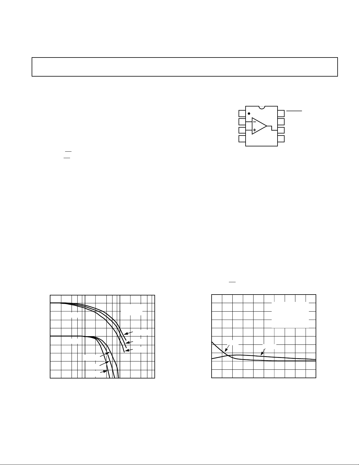
GAIN
PHASE
GAIN = +2
R
F
= 715Ω
R
L
= 150Ω
f
C
= 3.58MHz
100 IRE
MODULATED RAMP
SUPPLY VOLTAGE – ± Volts
DIFFERENTIAL GAIN – %
DIFFERENTIAL PHASE – Degrees
a
FEATURES
High Speed
80 MHz Bandwidth (3 dB, G = +1)
75 MHz Bandwidth (3 dB, G = +2)
1000 V/ms Slew Rate
50 ns Settling Time to 0.1% (V
Ideal for Video Applications
30 MHz Bandwidth (0.1 dB, G = +2)
0.02% Differential Gain
0.048 Differential Phase
Low Noise
2.9 nV/√
13 pA/√
Hz Input Voltage Noise
Hz Inverting Input Current Noise
Low Power
8.0 mA Supply Current max
2.1 mA Supply Current (Power-Down Mode)
High Performance Disable Function
Turn-Off Time 100 ns
Break Before Make Guaranteed
Input to Output Isolation of 64 dB (OFF State)
Flexible Operation
Specified for 65 V and 615 V Operation
62.9 V Output Swing Into a 150 V Load (V
APPLICATIONS
Professional Video Cameras
Multimedia Systems
NTSC, PAL & SECAM Compatible Systems
Video Line Driver
ADC/DAC Buffer
DC Restoration Circuits
= 10 V Step)
O
= 65 V)
S
Video Op Amp with Disable
AD810
CONNECTION DIAGRAM
8-Pin Plastic Mini-DIP (N), SOIC (R)
and Cerdip (Q) Packages
OFFSET
PRODUCT DESCRIPTION
The AD810 is a composite and HDTV compatible, current
feedback, video operational amplifier, ideal for use in systems
such as multimedia, digital tape recorders and video cameras.
The 0.1 dB flatness specification at bandwidth of 30 MHz
(G = +2) and the differential gain and phase of 0.02% and
0.04° (NTSC) make the AD810 ideal for any broadcast quality
video system. All these specifications are under load conditions
of 150 Ω (one 75 Ω back terminated cable).
The AD810 is ideal for power sensitive applications such as
video cameras, offering a low power supply current of 8.0 mA
max. The disable feature reduces the power supply current to
only 2.1 mA, while the amplifier is not in use, to conserve
power. Furthermore the AD810 is specified over a power supply
range of ±5 V to ±15 V.
The AD810 works well as an ADC or DAC buffer in video
systems due to its unity gain bandwidth of 80 MHz. Because the
AD810 is a transimpedance amplifier, this bandwidth can be
maintained over a wide range of gains while featuring a low
noise of 2.9 nV/√
NULL
–IN
+IN
–V
1
AD810
2
3
4
S
TOP VIEW
8
7
6
5
DISABLE
+V
S
OUTPUT
OFFSET
NULL
Hz for wide dynamic range applications.
REV. A
Information furnished by Analog Devices is believed to be accurate and
reliable. However, no responsibility is assumed by Analog Devices for its
use, nor for any infringements of patents or other rights of third parties
which may result from its use. No license is granted by implication or
otherwise under any patent or patent rights of Analog Devices.
GAIN = +2
R
= 150Ω
PHASE
1
0
–1
–2
–3
–4
CLOSED-LOOP GAIN – dB
–5
1 1000
Closed-Loop Gain and Phase vs. Frequency, G = +2,
= 150, RF = 715
R
L
GAIN
VS = ±15V
±2.5V
10 100
FREQUENCY – MHz
Ω
±5V
L
VS = ±15V
±5V
±2.5V
0
–45
–90
–135
–180
–225
PHASE SHIFT – Degrees
–270
Differential Gain and Phase vs. Supply Voltage
One Technology Way, P.O. Box 9106, Norwood, MA 02062-9106, U.S.A.
Tel: 617/329-4700 Fax: 617/326-8703
Page 2

AD810–SPECIFICA TIONS
(@ TA = +258C and VS = 615 V dc, RL = 150 V unless otherwise noted)
1
Parameter Conditions V
AD810A AD810S
S
Min Typ Max Min Typ Max Units
DYNAMIC PERFORMANCE
3 dB Bandwidth (G = +2) R
(G = +2) R
(G = +1) R
(G = +10) R
0.1 dB Bandwidth (G = +2) R
(G = +2) R
Full Power Bandwidth V
Slew Rate
2
= 20 V p-p,
O
= 400 Ω±15 V 16 16 MHz
R
L
RL = 150 Ω±5 V 350 350 V/µs
= 400 Ω±15 V 1000 1000 V/µs
R
L
= 715 ±5 V 4050 4050 MHz
FB
= 715 ±15 V 5575 5575 MHz
FB
= 1000 ±15 V 4080 4080 MHz
FB
= 270 ±15 V 5065 5065 MHz
FB
= 715 ±5 V 1322 1322 MHz
FB
= 715 ±15 V 1530 1530 MHz
FB
Settling Time to 0.1% 10 V Step, G = –1 ±15 V 50 50 ns
Settling Time to 0.01% 10 V Step, G = –1 ±15 V 125 125 ns
Differential Gain f = 3.58 MHz ±15 V 0.02 0.05 0.02 0.05 %
f - 3.58 MHz ±5 V 0.04 0.07 0.04 0.07 %
Differential Phase f = 3.58 MHz ±15 V 0.04 0.07 0.04 0.07 Degrees
f = 3.58 MHz ±5 V 0.045 0.08 0.045 0.08 Degrees
Total Harmonic Distortion f = 10 MHz, V
= 2 V p-p
O
RL = 400 Ω, G = +2 ±15 V –61 –61 dBc
INPUT OFFSET VOLTAGE ±5 V, ±15 V 1.5 6 1.5 6 mV
T
MIN–TMAX
±5 V, ±15 V 2 7.5 4 15 mV
Offset Voltage Drift 715µV/°C
INPUT BIAS CURRENT
–Input T
+Input T
OPEN-LOOP T
MIN–TMAX
MIN–TMAX
MIN–TMAX
±5 V, ±15 V 0.7 5 0.8 5 µA
±5 V, ±15 V 2 7.5 2 10 µA
TRANSRESISTANCE VO = ±10 V, RL = 400 Ω±15 V 1.0 3.5 1.0 3.5 MΩ
VO = ±2.5 V, RL = 100 Ω±5 V 0.3 1.2 0.2 1.0 MΩ
OPEN-LOOP T
MIN–TMAX
DC VOLTAGE GAIN VO = ±10 V, RL = 400 Ω±15 V 86 100 80 100 dB
VO = ±2.5 V, RL = 100 Ω±5 V 7688 7288 dB
COMMON-MODE REJECTION T
V
OS
±Input Current T
MIN–TMAX
VCM = ±12 V ±15 V 5664 5664 dB
= ±2.5 V ±5 V 5260 5060 dB
V
CM
MIN–TMAX
±5 V, ±15 V 0.1 0.4 0.1 0.4 µA/V
POWER SUPPLY REJECTION ±4.5 V to ±18 V
V
OS
±Input Current T
T
MIN–TMAX
MIN–TMAX
65 72 60 72 dB
0.05 0.3 0.05 0.3 µA/V
INPUT VOLTAGE NOISE f = 1 kHz ±5 V, ±15 V 2.9 2.9 nV/√Hz
INPUT CURRENT NOISE –I
, f = 1 kHz ±5 V, ±15 V 13 13 pA/√Hz
IN
+IIN, f = 1 kHz ±5 V, ±15 V 1.5 1.5 pA/√Hz
INPUT COMMON-MODE ±5 V ±2.5 ±3.0 ±2.5 ±3V
VOLTAGE RANGE ±15 V ±12 ±13 ±12 ±13 V
OUTPUT CHARACTERISTICS
Output Voltage Swing
3
RL = 150 Ω, T
= 400 Ω±15 V ±12.5 ±12.9 ±12.5 ±12.9 V
R
L
= 400 Ω, T
R
L
MIN–TMAX
MIN–TMAX
±5 V ±2.5 ±2.9 ±2.5 ±2.9 V
±15 V ±12 ±12 V
Short-Circuit Current ±15 V 150 150 mA
Output Current T
MIN–TMAX
±5 V, ±15 V 4060 3060 mA
OUTPUT RESISTANCE Open Loop (5 MHz) 15 15 Ω
INPUT CHARACTERISTICS
Input Resistance +Input ±15 V 2.5 10 2.5 10 MΩ
–Input ±15 V 40 40 Ω
Input Capacitance +Input ±15 V 2 2 pF
DISABLE CHARACTERISTICS
4
OFF Isolation f = 5 MHz, See Figure 43 64 64 dB
OFF Output Impedance See Figure 43 (RF + RG)i13 pF (RF+ RG)i13 pF
–2–
REV. A
Page 3
AD810
1
Parameter Conditions V
Turn On Time
Turn Off Time Z
5
Z
= Low, See Figure 54 170 170 ns
OUT
= High 100 100 ns
OUT
AD810A AD810S
S
Min Typ Max Min Typ Max Units
Disable Pin Current Disable Pin = 0 V ±5 V 5075 5075µA
±15 V 290 400 290 400 µA
Min Disable Pin Current to
Disable T
MIN–TMAX
±5 V, ±15 V 30 30 µA
POWER SUPPLY
Operating Range +25°C to T
T
MIN
MAX
±2.5 ±18 ±2.5 ±18 V
±3.0 ±18 ±3.5 ±18 V
Quiescent Current ±5 V 6.7 7.5 6.7 7.5 mA
±15 V 6.8 8.0 6.8 8.0 mA
T
MIN–TMAX
±5 V, ±15 V 8.3 10.0 9 11.0 mA
Power-Down Current ±5 V 1.8 2.3 1.8 2.3 mA
±15 V 2.1 2.8 2.1 2.8 mA
NOTES
1
See Analog Devices Military Data Sheet for 883B Specifications.
2
Slew rate measurement is based on 10% to 90% rise time with the amplifier configured for a gain of –10.
3
Voltage Swing is defined as useful operating range, not the saturation range.
4
Disable guaranteed break before make.
5
Turn On Time is defined with ±5 V supplies using complementary o utput CMOS to drive the disable pin.
Specifications subject to change without notice.
ABSOLUTE MAXIMUM RATINGS
Supply Voltage . . . . . . . . . . . . . . . . . . . . . . . . . . . . . . . .±18 V
Internal Power Dissipation
2
. . . . . . . Observe Derating Curves
Output Short Circuit Duration . . . . Observe Derating Curves
Common-Mode Input Voltage . . . . . . . . . . . . . . . . . . . . . .±V
Differential Input Voltage . . . . . . . . . . . . . . . . . . . . . . . .±6 V
Storage Temperature Range
Plastic DIP . . . . . . . . . . . . . . . . . . . . . . . . –65°C to +125°C
Cerdip . . . . . . . . . . . . . . . . . . . . . . . . . . . –65°C to +150°C
Small Outline IC . . . . . . . . . . . . . . . . . . . –65°C to +125°C
Operating Temperature Range
AD810A . . . . . . . . . . . . . . . . . . . . . . . . . . . –40°C to +85°C
AD810S . . . . . . . . . . . . . . . . . . . . . . . . . . –55°C to +125°C
Lead Temperature Range (Soldering 60 sec) . . . . . . . +300°C
NOTES
1
Stresses above those listed under “Absolute Maximum Ratings” may cause
permanent damage to the device. This is a stress rating only and functional
operation of the device at these or any other conditions above those indicated in the
operational section of this specification is not implied. Exposure to absolute
maximum raring conditions for extended periods may affect device reliability.
2
8-Pin Plastic Package: θJA = 90°C/Watt; 8-Pin Cerdip Package: θJA = 110°C/Watt;
8-Pin SOIC Package: θJA = 150°C/Watt.
ESD SUSCEPTIBILITY
ESD (electrostatic discharge) sensitive device. Electrostatic
charges as high as 4000 volts, which readily accumulate on the
human body and on test equipment, can discharge without
detection. Although the AD810 features ESD protection
circuitry, permanent damage may still occur on these devices if
they are subjected to high energy electrostatic discharges.
Therefore, proper ESD precautions are recommended to avoid
any performance degradation or loss of functionality.
ORDERING GUIDE
Temperature Package Package
Model Range Description Option
AD810AN –40°C to +85°C 8-Pin Plastic DIP N-8
AD810AR –40°C to +85°C 8-Pin Plastic SOIC R-8
AD810AR-REEL –40°C to +85°C 8-Pin Plastic SOIC R-8
1
MAXIMUM POWER DISSIPATION
The maximum power that can be safely dissipated by the
AD810 is limited by the associated rise in junction temperature.
For the plastic packages, the maximum safe junction temperature is 145°C. For the cerdip package, the maximum junction
S
temperature is 175°C. If these maximums are exceeded momentarily, proper circuit operation will be restored as soon as the die
temperature is reduced. Leaving the device in the “overheated”
condition for an extended period can result in device burnout.
To ensure proper operation, it is important to observe the
derating curves.
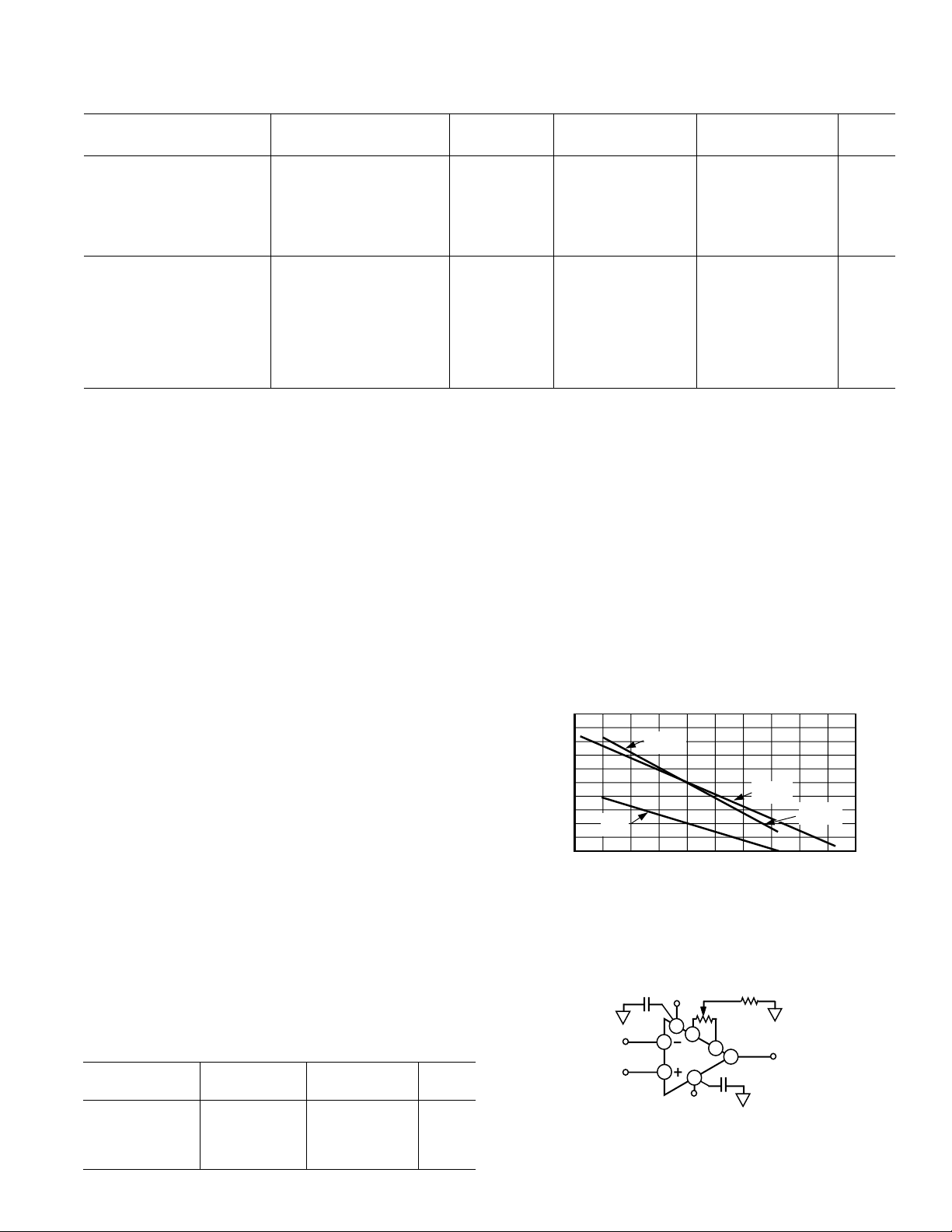
2.4
2.2
2.0
1.8
1.6
1.4
1.2
1.0
TOTAL POWER
0.8
DISSIPATION – Watts
0.6
0.4
–40
–60
8-PIN
MINI-DIP
8-PIN
SOIC
–20
AMBIENT TEMPERATURE –
8-PIN
CERDIP
°C
8-PIN
MINI-DIP
120100806040200
140
Maximum Power Dissipation vs. Temperature
While the AD810 is internally short circuit protected, this may
not be sufficient to guarantee that the maximum junction
temperature is not exceeded under all conditions.
0.1µF
+V
7
2
AD810
3
S
SEE TEXT
10kΩ
1
5
6
0.1µF
4
–V
S
Offset Null Configuration
5962-9313201MPA –55°C to +125°C 8-Pin Cerdip Q-8
REV. A
–3–
Page 4
AD810
10
4
140
7
5
–40
6
–60
9
8
120806040 100200–20
SUPPLY CURRENT – mA
JUNCTION TEMPERATURE – °C
VS = ±15V
VS = ±5V
–Typical Characteristics
20
15
NO LOAD
10
RL = 150Ω
5
MAGNITUDE OF THE OUTPUT VOLTAGE – ±Volts
0
020
51510
SUPPLY VOLTAGE – ±Volts
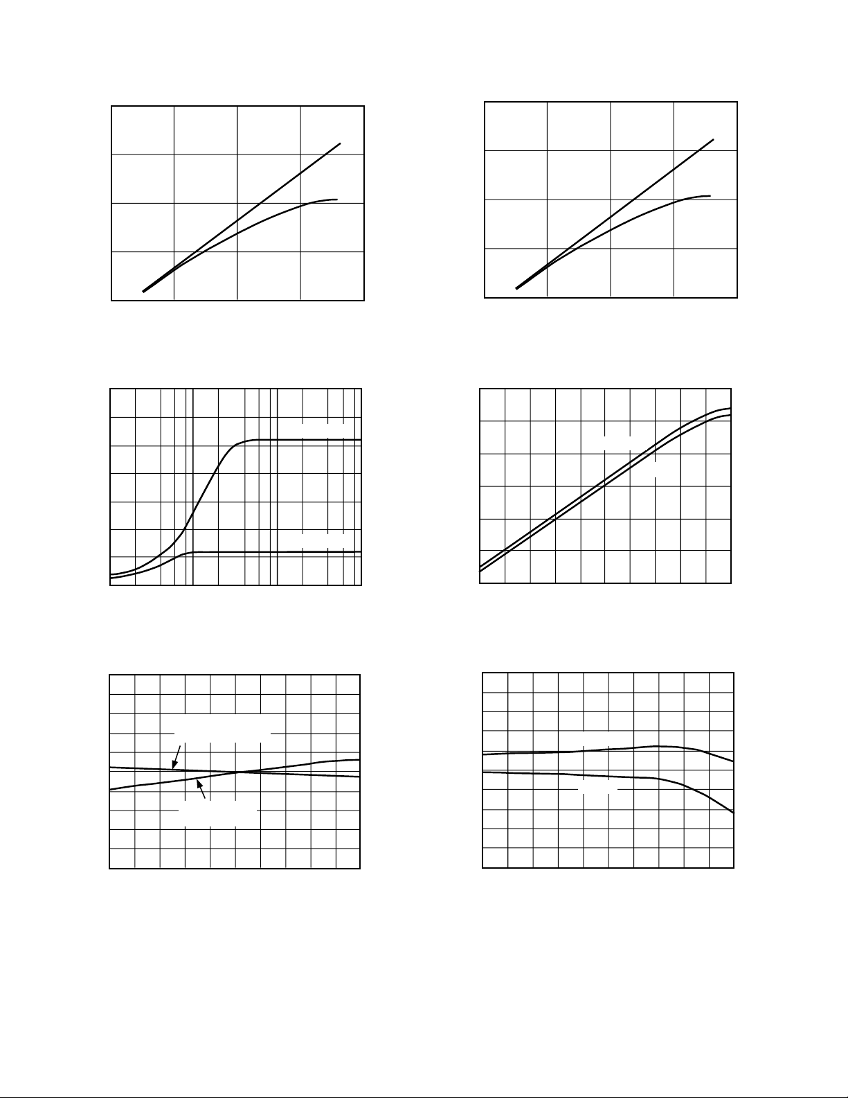
Figure 1. Input Common-Mode Voltage Range vs.
20
15
10
5
MAGNITUDE OF THE OUTPUT VOLTAGE – ±Volts
0
020
Figure 2. Output Voltage Swing vs. Supply
Supply Voltage
35
30
25
20
15
±15V SUPPLY
NO LOAD
RL = 150Ω
51510
SUPPLY VOLTAGE – ±Volts
10
OUTPUT VOLTAGE – Volts p-p
5
0
10 100 10k1k
LOAD RESISTANCE – Ohms
Figure 3. Output Voltage Swing vs. Load Resistance
10
8
6
4
2
0
–2
–4
INPUT BIAS CURRENT – µA
–6
–8
–10
Figure 5. Input Bias Current vs. Temperature
NONINVERTING INPUT
= ±5V, ±15V
V
S
INVERTING INPUT
V
= ±5V, ±15V
S
–20
0
JUNCTION TEMPERATURE – °C
±5V SUPPLY
Figure 4. Supply Current vs. Junction Temperature
10
8
6
4
2
0
–2
–4
INPUT OFFSET VOLTAGE – mV
–6
–8
–10
140–40–60 12010080604020
–40–60
VS = ±5V
VS = ±15V
JUNCTION TEMPERATURE – °C
140
120100806040200–20
Figure 6. Input Offset Voltage vs. Junction Temperature
–4–
REV. A
Page 5
Typical Characteristics–
100k
10k
1k
100
100k 1M 10M 100M
OUTPUT RESISTANCE – Ω
FREQUENCY – Hz
1M
100
10
1
100
10
1
10 100 1k 10k 100k
INVERTING INPUT
CURRENT NOISE
VOLTAGE NOISE
FREQUENCY – Hz
V
S
= ±5V TO ±15V
NONINVERTING INPUT
CURRENT NOISE
CURRENT NOISE – pA/ Hz
VOLTAGE NOISE – nV/ Hz
AD810
250
200
VS = ±15V
150
100
SHORT CIRCUIT CURRENT – mA
VS = ±5V
50
–60 +140
–40
JUNCTION TEMPERATURE – °C
+100 +120+80+60+40+200–20
Figure 7. Short Circuit Current vs. Temperature
10.0
VS = ±5V
VS = ±15V
1.0
0.1
GAIN = 2
= 715Ω
R
F
120
100
80
60
OUTPUT CURRENT – mA
40
20
–40
–60
JUNCTION TEMPERATURE – °C
VS = 5V
VS = 15V
±
±
+140
+120+100+80+60+40+200–20
Figure 8. Linear Output Current vs. Temperature
CLOSED-LOOP OUTPUT RESISTANCE – Ω
0.01
10k
100k 100M10M1M
FREQUENCY – Hz
Figure 9. Closed-Loop Output Resistance vs. Frequency
30
VS = ±15V
25
±
OUTPUT LEVEL FOR 3% THD
20
15
10
OUTPUT VOLTAGE – Volts p-p
5
0
Figure 11. Large Signal Frequency Response
= 400Ω
R
L
VS = ±5V
100k 1M 100M10M
FREQUENCY – Hz
Figure 10. Output Resistance vs. Frequency,
Disabled State
Figure 12. Input Voltage and Current Noise vs. Frequency
REV. A
–5–
Page 6

AD810
80
40
100k 100M10M1M10k
20
60
50
30
10
70
POWER SUPPLY REJECTION – dB
FREQUENCY – Hz
CURVES ARE FOR WORST CASE
CONDITION WHERE ONE SUPPLY
IS VARIED WHILE THE OTHER IS
HELD CONSTANT
R
F
= 715Ω
A
V
= +2
VS = ±15V
VS = ±5V
1200
200
2
400
800
600
1000
181614121086
4
SLEW RATE – V/µs
SUPPLY VOLTAGE – ±Volts
RL = 400Ω
GAIN = –10
GAIN = +10
GAIN = +2
–Typical Characteristics
100
90
80
70
60
50
40
COMMON-MODE REJECTION – dB
30
20
10k
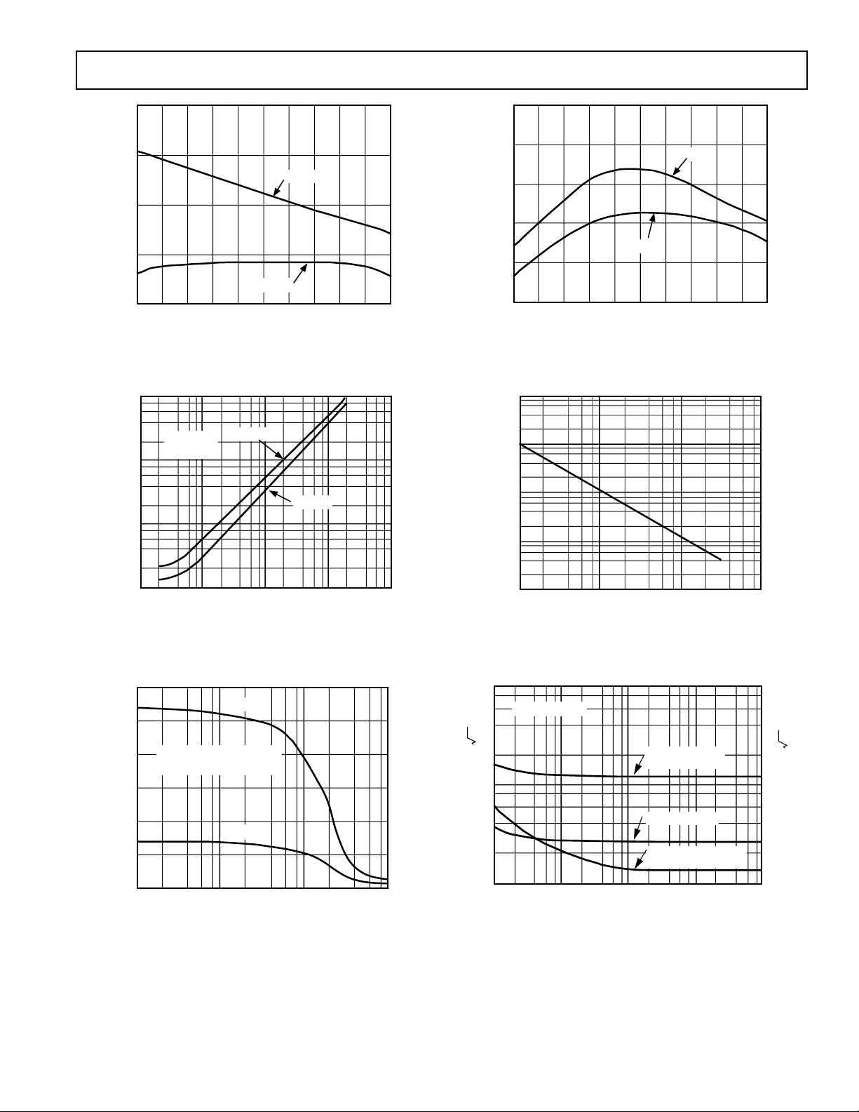
Figure 13. Common-Mode Rejection vs. Frequency
–40
–60
–80
–100
HARMONIC DISTORTION – dBc
2nd
3rd
–120
100 1k 10M1M100k10k
Figure 15. Harmonic Distortion vs. Frequency (RL = 100 Ω)
10
8
6
4
2
0
–2
–4
–6
OUTPUT SWING FROM ±V TO 0V
–8
–10
0
20
Figure 17. Output Swing and Error vs. Settling Time
100k 100M10M1M
VO = 2V p-p
= 100Ω
R
L
GAIN = +2
2nd HARMONIC
3rd HARMONIC
0.1%
0.1%
FREQUENCY – Hz
VS = ±5V
FREQUENCY – Hz
0.01%
SETTLING TIME – ns
V
S
0.01%
RF = RG = 1kΩ
= 400Ω
R
L
= ±15V
Figure 14. Power Supply Rejection vs. Frequency
–40
±15V SUPPLIES
–60
GAIN = +2
RL = 400Ω
–80
2nd HARMONIC
–100
3rd HARMONIC
HARMONIC DISTORTION – dBc
–120
2nd
3rd
–140
100 1k 10M1M100k10k
V
= 20V p-p
OUT
FREQUENCY – Hz
V
OUT
= 2V p-p
Figure 16. Harmonic Distortion vs. Frequency (RL = 400 Ω)
180160140120100806040
200
Figure 18. Slew Rate vs. Supply Voltage
–6–
REV. A
Page 7

1V
1V
0%
10
20nS
90
100
V
IN
V
O
200
60
20
40
120
80
100
140
160
180
–3dB BANDWIDTH – MHz
21816141210864
SUPPLY VOLTAGE – ±Volts
PEAKING 1dB
PEAKING 0.1dB
RF = 750Ω
RF = 1kΩ
RF = 1.5kΩ
G = +1
R
L
= 1kΩ
V
O
= 250mV p-p
≤
≤
V
IN
HP8130
PULSE
GENERATOR
Typical Characteristics, Noninverting Connection–
R
F
+V
S
0.1µF
R
G
7
AD810
323
4
0.1µF
50Ω
–V
S
6
V
TO
O
TEKTRONIX
P6201 FET
PROBE
R
L
V
O
AD810
Figure 21. Closed-Loop Gain and Phase vs. Frequency,
G= +1. R
REV. A
Figure 19. Noninverting Amplifier Connection
GAIN = +1
R
= 150Ω
RF = 1.5kΩ
L
VS = ±15V
±5V
±2.5V
PEAKING 1dB
PEAKING 0.1 dB
≤
≤
PHASE
1
0
–1
–2
–3
–4
CLOSED-LOOP GAIN – dB
–5
GAIN
VS = ±15V
±5V
±2.5V
1 1000
= 1 kΩ for ±15 V, 910 Ω for ±5 V and ±2.5 V
F
110
100
90
80
70
60
50
40
–3dB BANDWIDTH – MHz
30
20
Figure 23. Bandwidth vs. Supply Voltage,
Gain = +1, R
10 100
FREQUENCY – MHz
G = +1
R
= 150Ω
L
V
= 250mV p-p
O
21816141210864
= 150
L
RF = 750Ω
RF = 1kΩ
SUPPLY VOLTAGE – ±Volts
Ω
0
–45
–90
–135
–180
–225
PHASE SHIFT – Degrees
–270
Figure 20. Small Signal Pulse Response, Gain = +1,
= 1 kΩ, RL = 150 Ω, VS = ±15 V
R
F
GAIN = +1
R
= 1kΩ
PHASE
1
0
–1
–2
–3
–4
CLOSED-LOOP GAIN – dB
–5
GAIN
VS = ±15V
±5V
±2.5V
1 1000
10 100
FREQUENCY – MHz
L
VS = ±15V
±5V
±2.5V
Figure 22. Closed-Loop Gain and Phase vs. Frequency,
G= +1, R
= 1 kΩ for ±15 V, 910 Ω for ±5 V and ±2.5 V
F
Figure 24. –3 dB Bandwidth vs. Supply Voltage
= 1 k
G = +1, R
Ω
L
–7–
0
–45
–90
–135
–180
–225
PHASE SHIFT – Degrees
–270
Page 8

AD810
90
100
0%
10V
1V
10
50nS
V
IN
V
O
20
15
10 100
19
18
17
16
21
1
1000
0
–45
–90
–135
–180
–225
–270
CLOSED-LOOP GAIN – dB
PHASE SHIFT– Degrees
FREQUENCY – MHz
GAIN = +10
R
F
= 270Ω
R
L
= 1kΩ
VS = ±15V
±5V
±2.5V
VS = ±15V
±5V
±2.5V
PHASE
GAIN
40
20
2
30
70
50
60
80
90
100
1816141210864
–3dB BANDWIDTH – MHz
SUPPLY VOLTAGE – ±Volts
PEAKING 0.5dB
PEAKING 0.1dB
RF = 232Ω
RF = 442Ω
RF = 1kΩ
≤
≤
G = +10
RL = 1kΩ
V
O
= 250m V p-p
–Typical Characteristics, Noninverting Connection
100mV
100
V
IN
90
V
O
10
0%
1V
20nS
Figure 25. Small Signal Pulse Response, Gain = +10,
= 442 Ω, RL = 150 Ω, VS = ±15 V
R
F
PHASE
21
20
19
18
17
16
CLOSED-LOOP GAIN – dB
15
GAIN
VS = ±15V
1
±5V
±2.5V
10 100
FREQUENCY – MHz
GAIN = +10
R
= 270Ω
F
= 150Ω
R
L
VS = ±15V
±5V
±2.5V
0
–45
–90
–135
–180
–225
–270
1000
Figure 26. Large Signal Pulse Response, Gain = +10,
= 442 Ω, RL = 400 Ω, VS = ±15 V
R
F
PHASE SHIFT – Degrees
Figure 27. Closed-Loop Gain and Phase vs. Frequency,
G = +10, R
Figure 29. –3 dB Bandwidth vs. Supply Voltage,
Gain = +10, R
= 150
G = +10
= 150Ω
R
L
V
= 250mV p-p
O
2
Ω
L
100
90
80
70
60
50
–3dB BANDWIDTH – MHz
40
30
20
= 150
L
PEAKING 0.5dB
RF = 232Ω
PEAKING 0.1dB
RF = 442Ω
RF = 1kΩ
SUPPLY VOLTAGE – ±Volts
Ω
≤
≤
1816141210864
Figure 28. Closed-Loop Gain and Phase vs. Frequency,
G = +10, R
= 1 k
L
Ω
Figure 30. –3 dB Bandwidth vs. Supply Voltage,
Gain = +10, R
= 1 k
L
Ω
–8–
REV. A
Page 9

Typical Characteristics, Inverting Connection–
180
135
90
45
0
–45
–90
0
–5
10 100
–1
–2
–3
–4
1
1 1000
GAIN = –1
R
L
= 1kΩ
VS = ±15V
±5V
±2.5V
VS = ±15V
±5V
±2.5V
FREQUENCY – MHz
CLOSED-LOOP GAIN – dB
PHASE
GAIN
PHASE SHIFT – Degrees
60
20
2
40
120
80
100
140
160
180
1816141210864
–3dB BANDWIDTH – MHz
SUPPLY VOLTAGE – ±Volts
PEAKING 1.0dB
PEAKING 0.1dB
G = –1
R
L
= 1kΩ
V
O
= 250mV p-p
RF = 500Ω
RF = 649Ω
RF = 1kΩ
≤
≤
AD810
R
F
+V
S
V
IN
HP8130
PULSE
GENERATOR
0.1µF
R
G
7
AD810
323
4
0.1µF
–V
S
6
V
TO
O
TEKTRONIX
P6201 FET
PROBE
R
L
Figure 31. Inverting Amplifier Connection
GAIN = –1
= 150Ω
R
PHASE
1
0
–1
–2
–3
–4
CLOSED-LOOP GAIN – dB
–5
1
GAIN
VS = ±15V
±5V
±2.5V
10 100
FREQUENCY – MHz
L
VS = ±15V
±5V
±2.5V
V
1000
1V
100
V
90
IN
V
O
O
10
0%
20nS
1V
Figure 32. Small Signal Pulse Response, Gain = –1,
= 681 Ω, RL = 150 Ω, VS = ±5 V
R
F
180
135
90
45
0
–45
PHASE SHIFT – Degrees
–90
Figure 33. Closed-Loop Gain and Phase vs. Frequency
G = –1, R
and
REV. A
= 150 Ω, RF = 681 Ω for ±15 V, 620 Ω for ±5 V
L
±
2.5 V
G = –1
100
R
= 150
L
90
V
= 250mV p-p
O
80
70
60
50
40
–3dB BANDWIDTH – MHz
30
20
2
Figure 35. –3 dB Bandwidth vs. Supply Voltage,
Gain = –1, R
RF = 500Ω
RF = 681Ω
RF = 1kΩ
SUPPLY VOLTAGE – ±Volts
= 150
L
Ω
Figure 34. Closed-Loop Gain and Phase vs. Frequency,
G = –1, R
±
5 V and ±2.5 V
PEAKING 1.0dB
≤
PEAKING 0.1dB
≤
1816141210864
–9–
= 1 kΩ, RF = 681 Ω for VS = ±15 V, 620 Ω for
L
Figure 36. –3 dB Bandwidth vs. Supply Voltage,
Gain = –1, R
= 1 k
L
Ω
Page 10

AD810
90
0%
10V
1V
10
50nS
100
V
IN
V
O
–Typical Characteristics, Inverting Connection
100mV
100
V
90
IN
V
O
10
0%
20nS
1V
Figure 37. Small Signal Pulse Response, Gain = –10,
R
= 442 Ω, RL = 150 Ω, VS = ±15 V
F
180
PHASE
21
20
19
GAIN
18
17
16
CLOSED-LOOP GAIN – dB
15
1
VS = ±15V
GAIN = –10
= 249Ω
R
F
R
= 150Ω
L
VS = ±15V
±5V
±2.5V
±5V
±2.5V
10 100 1000
FREQUENCY – MHz
135
90
45
0
–45
–90
Figure 39. Closed-Loop Gain and Phase vs. Frequency,
= 150
G = –10, R
L
Ω
Figure 38. Large Signal Pulse Response, Gain = –10,
= 442 Ω, RL = 400 Ω, VS = ±15 V
R
F
PHASE SHIFT – Degrees
CLOSED-LOOP GAIN – dB
Figure 40. Closed-Loop Gain and Phase vs. Frequency,
G = –10, R
GAIN = –10
= 249Ω
R
PHASE
21
20
19
GAIN
18
17
16
15
1
= 1 k
L
VS = ±15V
±5V
±2.5V
10 100 1000
FREQUENCY – MHz
Ω
R
F
= 1kΩ
L
VS = ±15V
±5V
±2.5V
180
135
90
45
0
–45
PHASE SHIFT – Degrees
–90
100
G = –10
90
80
70
60
50
–3dB BANDWIDTH – MHz
40
30
20
Figure 41. –3 dB Bandwidth vs. Supply Voltage, G = –10,
R
= 150
L
Ω
= 150Ω
R
L
V
= 250mV p- p
O
21816141210864
RF = 249Ω
RF = 750Ω
SUPPLY VOLTAGE – ±Volts
NO PEAKING
RF = 442Ω
–10–
100
G = –10
90
= 1kΩ
R
L
V
= 250mV p- p
O
80
70
60
50
–3dB BANDWIDTH – MHz
40
30
20
2
RF = 249Ω
RF = 442Ω
RF = 750Ω
SUPPLY VOLTAGE – ±Volts
NO PEAKING
1816141210864
Figure 42. –3 dB Bandwidth vs. Supply Voltage, G = –10,
R
= 1 k
Ω
L
REV. A
Page 11

Applications–
AD810
GENERAL DESIGN CONSIDERATIONS
The AD810 is a current feedback amplifier optimized for use in
high performance video and data acquisition systems. Since it
uses a current feedback architecture, its closed-loop bandwidth
depends on the value of the feedback resistor. Table I below
contains recommended resistor values for some useful closedloop gains and supply voltages. As you can see in the table, the
closed-loop bandwidth is not a strong function of gain, as it
would be for a voltage feedback amp. The recommended
resistor values will result in maximum bandwidths with less than
0.1 dB of peaking in the gain vs. frequency response.
The –3 dB bandwidth is also somewhat dependent on the power
supply voltage. Lowering the supplies increases the values of
internal capacitances, reducing the bandwidth. To compensate
for this, smaller values of feedback resistor are sometimes used
at lower supply voltages. The characteristic curves illustrate that
bandwidths of over 100 MHz on 30 V total and over 50 MHz
on 5 V total supplies can be achieved.
Table I. –3 dB Bandwidth vs. Closed-Loop Gain and
Resistance Values (R
= 150 V)
L
VS = 615 V
Closed-Loop –3 dB BW
Gain R
FB
R
G
(MHz)
+1 1 kΩ 80
+2 715 Ω 715 Ω 75
+10 270 Ω 30 Ω 65
–1 681 Ω 681 Ω 70
–10 249 Ω 24.9 Ω 65
VS = 65 V
Closed-Loop –3 dB BW
Gain R
FB
R
G
(MHz)
+1 910 Ω 50
+2 715 Ω 715 Ω 50
+10 270 Ω 30 Ω 50
–1 620 Ω 620 Ω 55
–10 249 Ω 24.9 Ω 50
ACHIEVING VERY FLAT GAIN RESPONSE AT
HIGH FREQUENCY
Achieving and maintaining gain flatness of better than 0.1 dB
above 10 MHz is not difficult if the recommended resistor
values are used. The following issues should be considered to
ensure consistently excellent results.
CHOICE OF FEEDBACK AND GAIN RESISTOR
Because the 3 dB bandwidth depends on the feedback resistor,
the fine scale flatness will, to some extent, vary with feedback
resistor tolerance. It is recommended that resistors with a 1%
tolerance be used if it is desired to maintain exceptional flatness
over a wide range of production lots.
PRINTED CIRCUIT BOARD LAYOUT
As with all wideband amplifiers, PC board parasitics can affect
the overall closed-loop performance. Most important are stray
capacitances at the output and inverting input nodes. (An added
capacitance of 2 pF between the inverting input and ground will
add about 0.2 dB of peaking in the gain of 2 response, and
increase the bandwidth to 105 MHz.) A space (3/16" is plenty)
should be left around the signal lines to minimize coupling.
Also, signal lines connecting the feedback and gain resistors
should be short enough so that their associated inductance does
not cause high frequency gain errors. Line lengths less than 1/4"
are recommended.
QUALITY OF COAX CABLE
Optimum flatness when driving a coax cable is possible only
when the driven cable is terminated at each end with a resistor
matching its characteristic impedance. If coax were ideal, then
the resulting flatness would not be affected by the length of the
cable. While outstanding results can be achieved using
inexpensive cables, some variation in flatness due to varying
cable lengths is to be expected.
POWER SUPPLY BYPASSING
Adequate power supply bypassing can be critical when
optimizing the performance of a high frequency circuit.
Inductance in the power supply leads can contribute to resonant
circuits that produce peaking in the amplifier's response. In
addition, if large current transients must be delivered to the
load, then bypass capacitors (typically greater than 1 µF) will be
required to provide the best settling time and lowest distortion.
Although the recommended 0.1 µF power supply bypass
capacitors will be sufficient in most applications, more elaborate
bypassing (such as using two paralleled capacitors) may be
required in some cases.
POWER SUPPLY OPERATING RANGE
The AD810 will operate with supplies from ± 18 V down to
about ±2.5 V. On ±2.5 V the low distortion output voltage
swing will be better than 1 V peak to peak. Single supply
operation can be realized with excellent results by arranging for
the input common-mode voltage to be biased at the supply
midpoint.
OFFSET NULLING
A 10 kΩ pot connected between Pins 1 and 5, with its wiper
connected to V+, can be used to trim out the inverting input
current (with about ±20 µA of range). For closed-loop gains
above about 5, this may not be sufficient to trim the output
offset voltage to zero. Tie the pot's wiper to ground through a
large value resistor (50 kΩ for ± 5 V supplies, 150 kΩ for ±15 V
supplies) to trim the output to zero at high closed-loop gains.
REV. A
–11–
Page 12

AD810
2k1k 4k3k
1
10
100
1000
LOAD CAPACITANCE – pF
FEEDBACK RESISTOR – Ω
0
VS = ±15V
GAIN = +2
R
L
= 1kΩ
VS = ±5V
90
100
0%
5V
5V 100nS
V
IN
V
OUT
CAPACITIVE LOADS
When used with the appropriate feedback resistor, the AD810
can drive capacitive loads exceeding 1000 pF directly without
oscillation. By using the curves in Figure 45 to chose the resistor
value, less than 1 dB of peaking can easily be achieved without
sacrificing much bandwidth. Note that the curves were
generated for the case of a 10 kΩ load resistor, for smaller load
resistances, the peaking will be less than indicated by Figure 45.
Another method of compensating for large load capacitances is
to insert a resistor in series with the loop output as shown in
Figure 43. In most cases, less than 50 Ω is all that is needed to
achieve an extremely flat gain response.
Figures 44 to 46 illustrate the outstanding performance that can
be achieved when driving a 1000 pF capacitor.
R
F
0.1µF
+V
S
R
G
V
IN
323
R
T
7
AD810
4
–V
S
1.0µF
1.0µF
0.1µF
6
RS (OPTIONAL)
C
L
V
O
R
L
Figure 45. Max Load Capacitance for Less than 1 dB of
Peaking vs. Feedback Resistor
Figure 43. Circuit Options for Driving a Large
Capacitive Load
9
6
3
0
–3
–6
CLOSED-LOOP GAIN – dB
–9
1 10 100
Figure 44. Performance Comparison of Two Methods for
Driving a Large Capacitive Load
RF = 4.5kΩ
R
FREQUENCY – MHz
G = +2
V
= ±15V
S
R
= 10kΩ
L
C
= 1000pF
L
RF = 750Ω
R
= 11Ω
= 0
S
S
Figure 46. AD810 Driving a 1000 pF Load,
Gain = +2, R
= 750 Ω, RS = 11 Ω, RL = 10 k
F
Ω
DISABLE MODE
By pulling the voltage on Pin 8 to common (0 V), the AD810
can be put into a disabled state. In this condition, the supply
current drops to less than 2.8 mA, the output becomes a high
impedance, and there is a high level of isolation from input to
output. In the case of a line driver for example, the output
impedance will be about the same as for a 1.5 kΩ resistor (the
feedback plus gain resistors) in parallel with a 13 pF capacitor
(due to the output) and the input to output isolation will be
better than 65 dB at 1 MHz.
Leaving the disable pin disconnected (floating) will leave the
AD810 operational in the enabled state.
In cases where the amplifier is driving a high impedance load,
the input to output isolation will decrease significantly if the
input signal is greater than about 1.2 V peak to peak. The
isolation can be restored back to the 65 dB level by adding a
dummy load (say 150 Ω) at the amplifier output. This will
attenuate the feedthrough signal. (This is not an issue for
multiplexer applications where the outputs of multiple AD810s
are tied together as long as at least one channel is in the ON
state.) The input impedance of the disable pin is about 35 kΩ in
parallel with a few pF. When grounded, about 50 µA flows out
–12–
REV. A
Page 13

AD810
of the disable the disable pin for ± 5 V supplies. If driven by
complementary output CMOS logic (such as the 74HC04), the
disable time (until the output goes high impedance) is about
100 ns and the enable time (to low impedance output) is about
170 ns on ±5 V supplies. The enable time can be extended to
about 750 ns by using open drain logic such as the 74HC05.
When operated on ±15 V supplies, the AD810 disable pin may
be driven by open drain logic such as the 74C906. In this case,
adding a 10 kΩ pull-up resistor from the disable pin to the plus
supply will decrease the enable time to about 150 ns. If there is
a nonzero voltage present on the amplifier's output at the time it
is switched to the disabled state, some additional decay time will
be required for the output voltage to relax to zero. The total
time for the output to go to zero will generally be about 250 ns
and is somewhat dependent on the load impedance.
OPERATION AS A VIDEO LINE DRIVER
The AD810 is designed to offer outstanding performance at
closed-loop gains of one or greater. At a gain of 2, the AD810
makes an excellent video line driver. The low differential gain
and phase errors and wide –0.1 dB bandwidth are nearly
independent of supply voltage and load (as seen in Figures 49
and 50).
323
715Ω
+V
S
7
AD810
4
–V
S
0.1µF
0.1µF
75Ω
CABLE
75Ω
6
75Ω
V
OUT
715Ω
75Ω
CABLE
V
IN
75Ω
Figure 47. A Video Line Driver Operating at a Gain of +2
GAIN = +2
R
= 150Ω
PHASE
1
0
–1
–2
–3
–4
CLOSED-LOOP GAIN – dB
–5
1 1000
GAIN
VS = ±15V
±5V
±2.5V
10 100
FREQUENCY – MHz
L
VS = ±15V
±5V
±2.5V
0
–45
–90
–135
–180
–225
PHASE SHIFT – Degrees
–270
0.10
0.09
0.08
0.07
0.06
0.05
0.04
DIFFERENTIAL GAIN – %
0.03
0.02
0.01
0
GAIN
6
5
GAIN = +2
= 715Ω
R
F
= 150Ω
R
L
= 3.58MHz
f
C
100 IRE
MODULATED RAMP
PHASE
SUPPLY VOLTAGE – ± Volts
0.20
0.18
0.16
0.14
0.12
0.10
0.08
0.06
0.04
DIFFERENTIAL PHASE – Degrees
0.02
0
15
1413121110987
Figure 49. Differential Gain and Phase vs. Supply Voltage
+0.1
0
–0.1
+0.1
0
NORMALIZED GAIN – dB
–0.1
100k
RL = 150Ω
±2.5
RL= 1k
1M 100M10M
FREQUENCY – Hz
±15V
±5V
±15V
±5V
±2.5
Figure 50. Fine-Scale Gain (Normalized) vs. Frequency
for Various Supply Voltages, Gain = +2, R
110
G = +2
100
= 150Ω
R
L
90
V
= 250mV p-p
O
80
70
60
50
40
–3dB BANDWIDTH – MHz
30
20
2
RF = 500
SUPPLY VOLTAGE - ±Volts
PEAKING 1.0dB
RF = 750
RF = 1k
= 715
F
≤
≤
PEAKING 0.1dB
1816141210864
Ω
Figure 48. Closed-Loop Gain and Phase vs. Frequency,
G = +2, R
= 150, RF = 715
L
Ω
REV. A
–13–
Figure 51. –3 dB Bandwidth vs. Supply Voltage,
Gain = +2, R
= 150
L
Ω
Page 14

AD810
AD810
7
323
0.1µF
+5V
6
VINA
750Ω
–5V
4
0.1µF
8
V
SW
V
OUT
75Ω
75Ω
CABLE
74HC04
AD810
7
323
0.1µF
+5V
6
VINB
–5V
4
0.1µF
8
75Ω
750Ω
750Ω 750Ω
75Ω
75Ω
–0.5
–3.0
1 10 100
–1.0
–1.5
–2.0
–2.5
0
0.5
0
–45
–90
–135
–180
–225
–270
PHASE
GAIN
CLOSED-LOOP GAIN – dB
PHASE SHIFT – Degrees
FREQUENCY – MHz
VS = ±5V
2:1 VIDEO MULTIPLEXER
The outputs of two AD810s can be wired together to form a
2:1 mux without degrading the flatness of the gain response.
Figure 54 shows a recommended configuration which results in
–0.1 dB bandwidth of 20 MHz and OFF channel isolation of
77 dB at 10 MHz on ±5 V supplies. The time to switch between
channels is about 0.75 µs when the disable pins are driven by
open drain output logic. Adding pull-up resistors to the logic
outputs or using complementary output logic (such as the
74HC04) reduces the switching time to about 180 ns. The
switching time is only slightly affected by the signal level.
500mV 500nS
100
90
10
0%
5V
Figure 54. A Fast Switching 2:1 Video Mux
Figure 52. Channel Switching Time for the 2:1 Mux
–40
–50
–60
–70
FEEDTHROUGH – dB
–80
–90
1 10 100
Figure 53. 2:1 Mux OFF Channel Feedthrough vs.
Frequency
FREQUENCY – MHz
–14–
Figure 55. 2:1 Mux ON Channel Gain and Phase vs.
Frequency
REV. A
Page 15

N:1 MULTIPLEXER
AD810
75Ω
7
2
3
0.1µF
+V
S
6
1kΩ
–V
S
4
0.1µF
8
SELECT A
AD810
7
2
3
0.1µF
+V
S
6
–V
S
4
0.1µF
8
SELECT D
AD810
7
2
3
0.1µF
+V
S
6
–V
S
4
0.1µF
8
SELECT C
AD810
7
2
3
0.1µF
+V
S
6
–V
S
4
0.1µF
8
SELECT B
33Ω
V
OUT
R
L
C
L
VIN, A
V
IN
, B
V
IN
, C
V
IN
, D
75Ω
1kΩ
33Ω
75Ω
1kΩ
33Ω
75Ω
1kΩ
33Ω
A multiplexer of arbitrary size can be formed by combining the
desired number of AD810s together with the appropriate
selection logic. The schematic in Figure 58 shows a
recommendation for a 4:1 mux which may be useful for driving
a high impedance such as the input to a video A/D converter
(such as the AD773). The output series resistors effectively
compensate for the combined output capacitance of the OFF
channels plus the input capacitance of the A/D while
maintaining wide bandwidth. In the case illustrated, the –0.1 dB
bandwidth is about 20 MHz with no peaking. Switching time
and OFF channel isolation (for the 4:1 mux) are about 250 ns
and 60 dB at 10 MHz, respectively.
AD810
PHASE
0.5
0
–0.5
–1.0
–1.5
–2.0
–2.5
CLOSED-LOOP GAIN – dB
–3.0
Figure 56. 4:1 Mux ON Channel Gain and Phase vs.
Frequency
Figure 57. 4:1 Mux OFF Channel Feedthrough vs.
Frequency
REV. A
VS = ±15V
RL = 10kΩ
C
= 10pF
L
1 10 100
–30
–40
–50
FEEDTHROUGH – dB
–60
–70
1 10 100
FREQUENCY – MHz
GAIN
FREQUENCY – MHz
0
–45
–90
–135
–180
PHASE SHIFT – Degrees
–225
–15–
Figure 58. A 4:1 Multiplexer Driving a High Impedance
Page 16

AD810
OUTLINE DIMENSIONS
Dimensions shown in inches and (mm).
Plastic Mini-DIP (N) Package
PIN 1
0.165 ±0.01
(4.19 ±0.25)
0.125
(3.18)
MIN
0.005 (0.13) MIN
PIN 1
0.200
(5.08)
MAX
0.200 (5.08)
0.125 (3.18)
8
1
0.018
±0.003
(0.46 ±0.08)
8
1
0.023 (0.58)
0.014 (0.36)
5
0.25
(6.35)
4
0.39 (9.91) MAX
0.10
(2.54)
BSC
0.033
(0.84)
NOM
0.035 ±0.01
(0.89 ±0.25)
0.18 ±0.03
(4.57 ±0.76)
SEATING
PLANE
Cerdip (Q) Package
0.055 (1.40) MAX
5
0.310 (7.87)
0.220 (5.59)
4
0.405 (10.29) MAX
0.100
(2.54)
BSC
0.070 (1.78)
0.030 (0.76)
0.060 (1.52)
0.015 (0.38)
SEATING
PLANE
(7.87)
0.150
(3.81)
MIN
0.31
0.30 (7.62)
REF
0.011 ±0.003
(0.28 ±0.08)
15
°
0
°
0.320 (8.13)
0.290 (7.37)
0.015 (0.38)
0.008 (0.20)
15
°
0
°
C1737–24–10/92
8-Pin SOIC (R) Package
0.150 (3.81)
PIN 1
8
1
0.050
(1.27)
BSC
0.244 (6.20)
0.228 (5.79)
0.010 (0.25)
0.004 (0.10)
All brand or product names mentioned are trademarks or registered trademarks of their respective holders.
0.197 (5.01)
0.189 (4.80)
0.019 (0.48)
0.014 (0.36)
5
4
0.157 (3.99)
0.150 (3.81)
0.102 (2.59)
0.094 (2.39)
0.098 (0.2482)
0.075 (0.1905)
0.020 (0.051) x 45
CHAMF
8
°
0
°
10
0
°
0.190 (4.82)
0.170 (4.32)
°
°
0.030 (0.76)
0.018 (0.46)
0.090
(2.29)
PRINTED IN U.S.A.
–16–
REV. A
 Loading...