

Page 1
Ultralow Distortion, High Speed
FEATURES
Ultralow noise: 0.95 nV/√Hz, 2.6 pA/√Hz
Ultralow distortion
nd
harmonic RL = 1 kΩ , G = +2
2
−92 dB @ 10 MHz
rd
3
harmonic RL = 1 kΩ , G = +2
−105 dB @ 10 MHz
High speed
GBWP: 3.8 GHz
–3 dB bandwidth:
700 MHz (G = +2)
550 MHz (G = +10)
Slew rate:
475 V/µs (G = +2)
1350 V/µs (G = +10)
New pinout
Custom external compensation, gain range –1, +2 to +10
Supply current: 15 mA
Offset voltage: 0.5 mV max
Wide supply voltage range: 5 V to 12 V
GENERAL DESCRIPTION
The AD8099 is an ultralow noise (0.95 nV/√Hz) and distortion
(–92 dBc @10 MHz) voltage feedback op amp, the combination
of which make it ideal for 16- and 18-bit systems. The AD8099
features a new, highly linear, low noise input stage that increases
the full power bandwidth (FPBW) at low gains with high slew
rates. ADI’s proprietary next generation XFCB process enables
such high performance amplifiers with relatively low power.
The AD8099 features external compensation, which lets the
user set the gain bandwidth product. External compensation
allows gains from +2 to +10 with minimal trade-off in bandwidth. The AD8099 also features an extremely high slew rate of
1350 V/µs, giving the designer flexibility to use the entire
dynamic range without trading off bandwidth or distortion.
The AD8099 settles to 0.1% in 18 ns and recovers from
overdrive in 50 ns.
The AD8099 drives 100 Ω loads at breakthrough performance
levels with only 15 mA of supply current. With the wide supply
voltage range (5 V to 12 V), low offset voltage (0.1 mV typ),
wide bandwidth (700 MHz for G = +2), and a GBWP up to
3.8 GHz, the AD8099 is designed to work in a wide variety of
applications.
0.95 nV/√Hz Voltage Noise Op Amp
AD8099
APPLICATIONS
Pre-amplifiers
Receivers
Instrumentation
Filters
IF and baseband amplifiers
A-to-D drivers
DAC buffers
Optical electronics
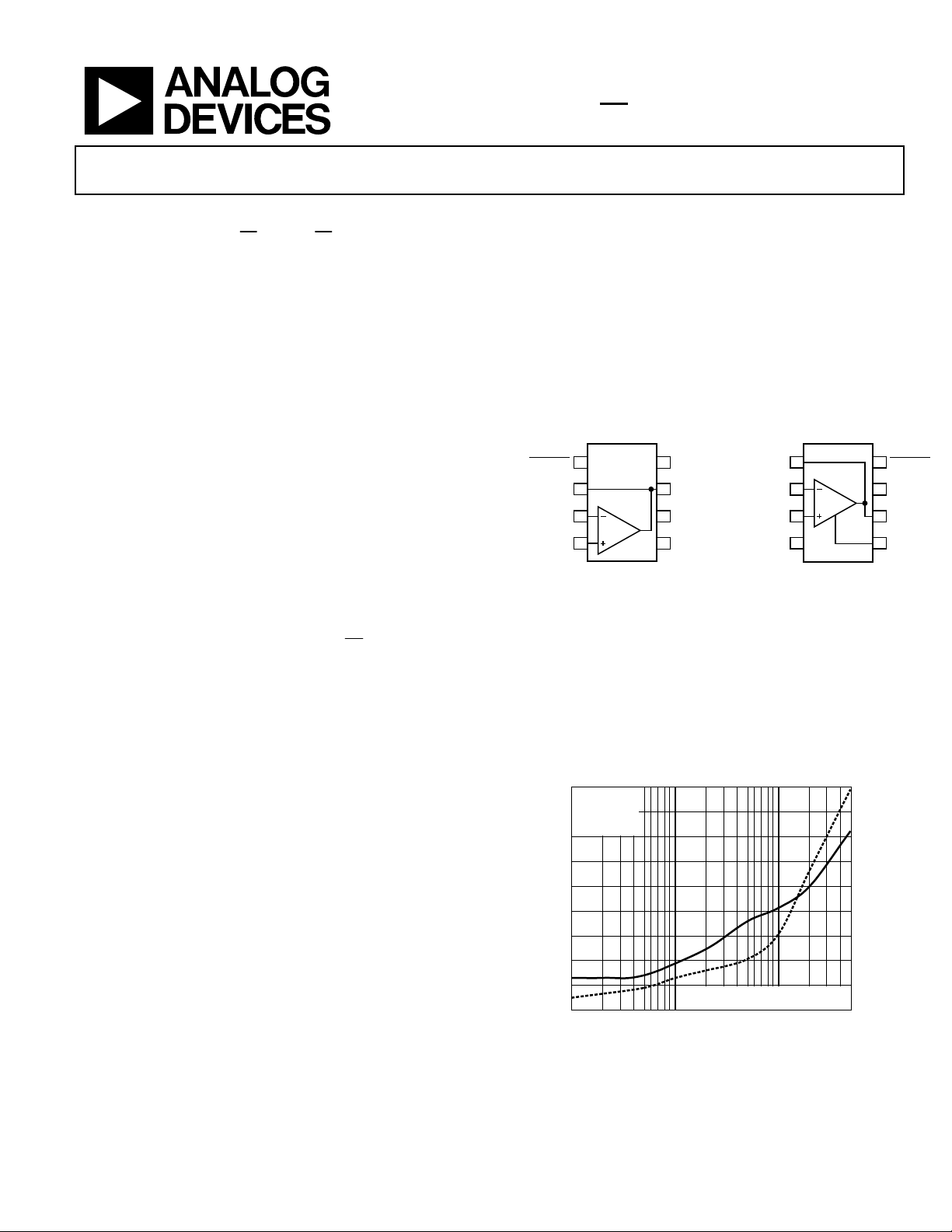
CONNECTION DIAGRAMS
–V
–IN
+IN
1
2
3
4
S
DISABLE
FEEDBACK
–IN
+IN
1
2
3
4
8
+V
S
7
V
OUT
6
C
C
5
–V
S
FEEDBACK
04511-0-001
Figure 1. 8-Lead CSP (CP-8) Figure 2. 8-Lead SOIC-ED (RD-8)
The AD8099 is available in a 3 mm × 3 mm lead frame chip
scale package (LFCSP) with a new pinout that is specifically
optimized for high performance, high speed amplifiers. The
new LFCSP package and pinout enable the breakthrough
performance that previously was not achievable with amplifiers.
The AD8099 is rated to work over the extended industrial
temperature range, −40°C to +125°C.
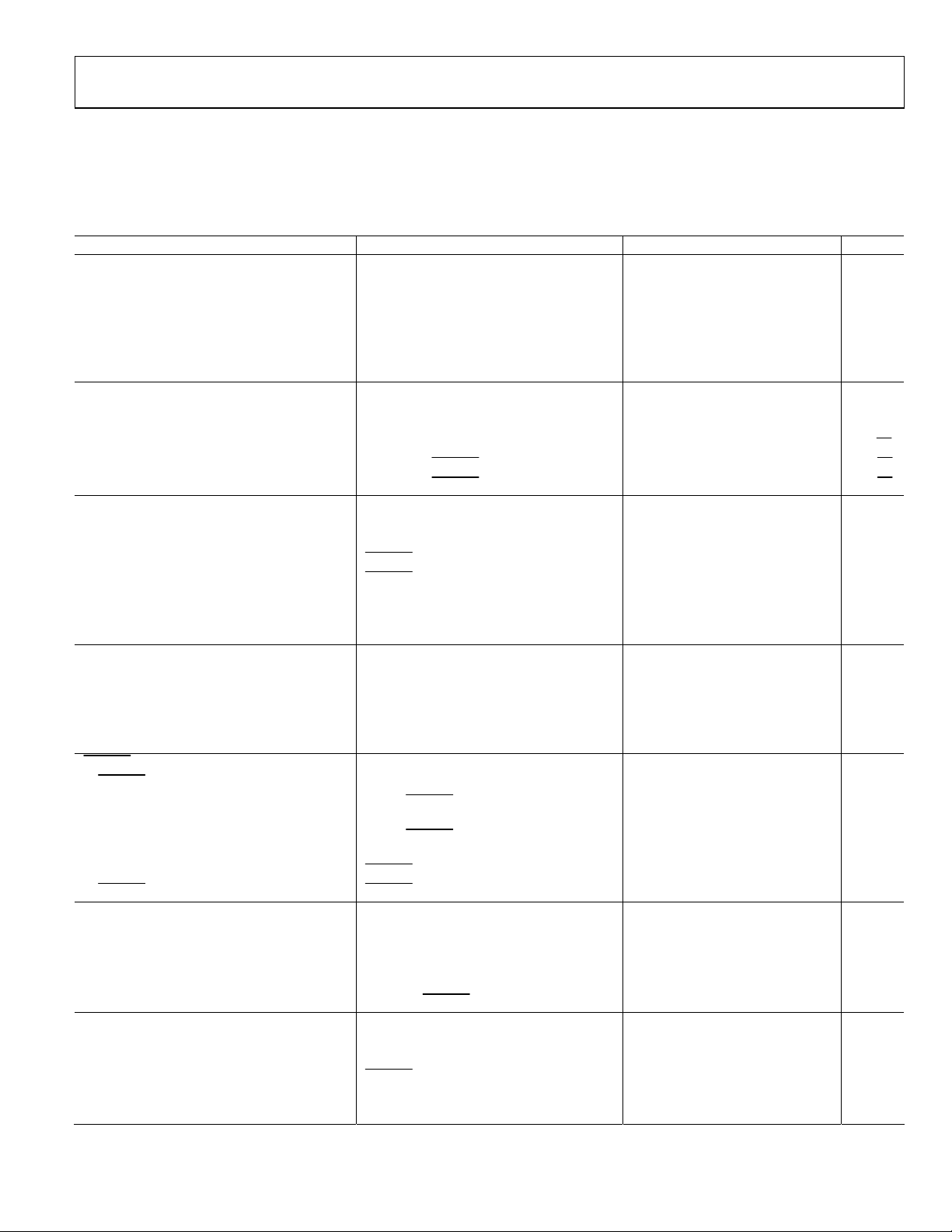
–40
G = +2
= 2V p-p
V
OUT
–50
V
= ±5V
S
R
= 1kΩ
L
–60
–70
–80
–90
–100
–110
HARMONIC DISTORTION (dBc)
–120
–130
0.1 1.0 10.0
Figure 3 . Harmonic Distortion vs. Frequency and Gain (SOIC)
SOLID LINE – SECOND HARMONIC
DOTTED LINE – THIRD HARMONIC
FREQUENCY (MHz)
8
DISABLE
7
+V
6
V
5
C
04511-A-013
S
OUT
C
04511-0-002
Rev. B
Information furnished by Analog Devices is believed to be accurate and reliable.
However, no responsibility is assumed by Analog Devices for its use, nor for any
infringements of patents or other rights of third parties that may result from its use.
Specifications subject to change without notice. No license is granted by implication
or otherwise under any patent or patent rights of Analog Devices. Trademarks and
registered trademarks are the property of their respective owners.
One Technology Way, P.O. Box 9106, Norwood, MA 02062-9106, U.S.A.
Tel: 781.329.4700
Fax: 781.326.8703 © 2004 Analog Devices, Inc. All rights reserved.
www.analog.com
Page 2

AD8099
TABLE OF CONTENTS
Specifications..................................................................................... 3
Specifications with ±5 V Supply................................................. 3
Specifications with +5 V Supply................................................. 4
Absolute Maximum Ratings............................................................ 5
Maximum Power Dissipation .....................................................5
ESD Caution.................................................................................. 5
Typical Performance Characteristics............................................. 6
Theory of Operation ...................................................................... 15
Applications..................................................................................... 16
Using the AD8099...................................................................... 16
Circuit Components...................................................................16
REVISION HISTORY
6/04—Data Sheet changed from REV. A to REV. B
Change to General Description...................................................... 1
Changes to Maximum Power Dissipation section ...................... 5
Changes to Applications section .................................................. 16
Changes to Table 7.......................................................................... 24
Changes to Ordering Guide.......................................................... 26
1/04—Data Sheet changed from REV. 0 to REV. A
Recommended Values ............................................................... 17
Circuit Configurations .............................................................. 17
Performance vs. Component values........................................ 19
Total Output Noise Calculations and Design......................... 20
Input Bias Current and DC Offset ........................................... 21
DISABLE
16-Bit ADC Driver..................................................................... 22
Circuit Considerations .............................................................. 23
Design Tools and Technical Support....................................... 23
Outline Dimensions .......................................................................25
Ordering Guide............................................................................... 26
Pin and Input Bias Cancellation............................. 21
Inserted new Figure 3................................................................... 1
Changes to Specifications............................................................ 3
Inserted new Figures 22 to 34..................................................... 8
Inserted new Figures 51 to 55................................................... 14
Changes to Theory of Operation section ................................16
Changes to Circuit Components section................................. 17
Changes to Table 4...................................................................... 18
Changes to Figure 60.................................................................. 18
Changes to Total Output Noise Calculations and
Design section........................................................................ 21
Changes to Figure 60.................................................................. 22
Changes to Figure 62.................................................................. 23
Changes to 16-Bit ADC Driver section................................... 23
Changes to Table 6...................................................................... 23
Additions to PCB Layout section ............................................. 23
11/03—Revision 0: Initial Version
Rev. B | Page 2 of 28
Page 3
AD8099
SPECIFICATIONS
SPECIFICATIONS WITH ±5 V SUPPLY
TA = 25°C, G = +2, RL = 1 kΩ to ground, unless otherwise noted. Refer to Figure 60 through Figure 66 for component values and
gain configurations .
Table 1.
Parameter Conditions Min Typ Max Unit
DYNAMIC PERFORMANCE
–3 dB Bandwidth G = +5, V
G = +5, V
Bandwidth for 0.1 dB Flatness (SOIC/CSP) G = +2, V
Slew Rate G = +10, V
G = +2, V
Settling Time to 0.1% G = +2, V
NOISE/DISTORTION PERFORMANCE
Harmonic Distortion (dBc) HD2/HD3 fC = 500 kHz, V
f
= 10 MHz, V
C
Input Voltage Noise f = 100 kHz 0.95
Input Current Noise
f = 100 kHz,
f = 100 kHz,
DC PERFORMANCE
Input Offset Voltage 0.1 0.5 mV
Input Offset Voltage Drift 2.3 µV/°C
Input Bias Current
DISABLE
DISABLE
Input Bias Current Drift 3 nA/°C
Input Bias Offset Current 0.06 1 µA
Open-Loop Gain 82 85 dB
INPUT CHARACTERISTICS
Input Resistance Differential mode 4 kΩ
Common mode 10 MΩ
Input Capacitance 2 pF
Input Common-Mode Voltage Range –3.7 to +3.7 V
Common-Mode Rejection Ratio VCM = ±2.5 V 98 105 dB
DISABLE
PIN
DISABLE
Input Voltage
Turn-Off Time
Turn-On Tim e
Enable Pin Leakage Current
DISABLE
Pin Leakage Current
Output disabled <2.4 V
50% of
= 0.5 V, G = +2
V
IN
50% of
= 0.5 V, G = +2
V
IN
DISABLE
DISABLE
OUTPUT CHARACTERISTICS
Output Overdrive Recovery Time (Rise/Fall) V
= -2.5 V to 2.5 V, G =+2 30/50 ns
IN
Output Voltage Swing RL = 100 Ω –3.4 to +3.5 –3.6 to +3.7 V
R
= 1 kΩ –3.7 to +3.7 –3.8 to +3.8 V
L
Short-Circuit Current Sinking and sourcing 131/178 mA
Off Isolation
f = 1 MHz,
POWER SUPPLY
Operating Range ±5 ±6 V
Quiescent Current 15 16 mA
Quiescent Current (Disabled)
DISABLE
Positive Power Supply Rejection Ratio +VS = 4 V to 6 V, –VS = –5 V (input referred) 85 91 dB
Negative Power Supply Rejection Ratio +VS = 5 V, –VS = –6 V to –4 V (input referred) 86 94 dB
= 0.2 V p-p 450 510 MHz
OUT
= 2 V p-p 205 235 MHz
OUT
= 0.2 V p-p 34/25 MHz
OUT
= 6 V Step 1120 1350 V/µs
OUT
= 2 V Step 435 470 V/µs
OUT
= 2 V Step 18 ns
OUT
= 2 V p-p, G = +10 –102/–111 dBc
OUT
= 2 V p-p, G = +10 –84/–92 dBc
OUT
DISABLE
DISABLE
pin floating
pin = +V
DISABLE
to < 10% of final V
pin floating
pin = +V
S
S
,
OUT
2.6
5.2
–6 –13 µA
–0.1 –2 µA
105 ns
DISABLE
=+5 V
= –5 V
DISABLE
= Low
to < 10% of final V
= low
OUT
,
39 ns
17 21 µA
35 44 µA
–61 dB
1.7 2 mA
Hz
nV/√
pA/√Hz
Hz
pA/√
Rev. B | Page 3 of 28
Page 4
AD8099
SPECIFICATIONS WITH +5 V SUPPLY
VS = 5 V @ TA = 25°C, G = +2, RL = 1 kΩ to midsupply, unless otherwise noted. Refer to Figure 60 through Figure 66 for component
values and gain configurations .
Table 2.
Parameter Conditions Min Typ Max Unit
DYNAMIC PERFORMANCE
–3 dB Bandwidth G = +5, V
G = +5, V
Bandwidth for 0.1 dB Flatness (SOIC/CSP) G = +2, V
Slew Rate G = +10, V
G = +2, V
Settling Time to 0.1% G = +2, V
NOISE/DISTORTION PERFORMANCE
Harmonic Distortion (dBc) HD2/HD3 fC = 500 kHz, V
f
= 10 MHz, V
C
Input Voltage Noise f = 100 kHz 0.95
Input Current Noise
f = 100 kHz,
f = 100 kHz,
DC PERFORMANCE
Input Offset Voltage 0.1 0.5 mV
Input Offset Voltage Drift 2.5 µV/°C
Input Bias Current
DISABLE
DISABLE
Input Bias Offset Current 0.05 1 µA
Input Bias Offset Current Drift 2.4 nA/°C
Open-Loop Gain V
OUT
INPUT CHARACTERISTICS
Input Resistance Differential mode 4 kΩ
Common mode 10 MΩ
Input Capacitance 2 pF
Input Common-Mode Voltage Range 1.3 to 3.7 V
Common-Mode Rejection Ratio VCM = 2 V to 3 V 88 105 dB
DISABLE
PIN
DISABLE
Input Voltage
Turn-Off Time
Turn-On Tim e
Enable Pin Leakage Current
DISABLE
Pin Leakage Current
Output disabled <2.4 V
50% of
= 0.5 V, G = +2
V
IN
50% of
= 0.5 V, G = +2
V
IN
DISABLE
DISABLE
OUTPUT CHARACTERISTICS
Overdrive Recovery Time (Rise/Fall) VIN = 0 to 2.5 V, G = +2 50/70 ns
Output Voltage Swing RL = 100 Ω 1.5 to 3.5 1.2 to 3.8 V
R
= 1 kΩ 1.2 to 3.8 1.2 to 3.8 V
L
Short-Circuit Current Sinking and Sourcing 60/80 mA
Off Isolation
f = 1 MHz,
POWER SUPPLY
Operating Range ±5 ±6 V
Quiescent Current 14.5 15.4 mA
Quiescent Current (Disabled)
DISABLE
Positive Power Supply Rejection Ratio +VS = 4.5 V to 5.5 V, –VS = 0 V (input referred) 84 89 dB
Negative Power Supply Rejection Ratio +VS =5 V, -VS= –0.5 V to +0.5 V (input referred) 84 90 dB
= 0.2 V p-p 415 440 MHz
OUT
= 2 V p-p 165 210 MHz
OUT
= 0.2 V p-p 33/23 MHz
OUT
= 2 V Step 630 715 V/µs
OUT
= 2 V Step 340 365 V/µs
OUT
= 2 V Step 18 ns
OUT
= 1 V p-p, G = +10 –82/–94 dBc
OUT
= 1 V p-p, G = +10 –80/–75 dBc
OUT
nV/√
DISABLE
DISABLE
pin floating
pin = +V
S
pin floating
pin = +V
S
2.6
5.2
pA/√Hz
pA/√
–6.2 –13 µA
–0.2 –2 µA
= 1 V to 4 V 76 81 dB
DISABLE
DISABLE
= 5 V
= 0 V
DISABLE
= Low
to <10% of Final V
to <10% of Final V
= Low
OUT
OUT
,
,
105 ns
61 ns
16 21 µA
33 44 µA
–61 dB
1.4 1.7 mA
Hz
Hz
Rev. B | Page 4 of 28
Page 5
AD8099
(
)
(
ABSOLUTE MAXIMUM RATINGS
Table 3.
Parameter Rating
Supply Voltage 12.6 V
Power Dissipation See Figure 4
Differential Input Voltage ±1.8 V
Differential Input Current ±10mA
Storage Temperature –65°C to +125°C
Operating Temperature Range –40°C to +125°C
Lead Temperature Range (Soldering 10 sec) 300°C
Junction Temperature 150°C
Stresses above those listed under Absolute Maximum Ratings
may cause permanent damage to the device. This is a stress
rating only; functional operation of the device at these or any
other conditions above those indicated in the operational
section of this specification is not implied. Exposure to absolute
maximum rating conditions for extended periods may affect
device reliability.
The difference between the total drive power and the load
power is the drive power dissipated in the package.
PD = Quiescent Power + (Total Drive Power – Load Power)
⎛
V
()
D
⎜
IVP
SS
⎜
⎝
2
⎞
V
OUTS
⎟
×+×=
⎟
R
L
⎠
RMS output voltages should be considered. If
V
–, as in single-supply operation, then the total drive power is
S
V
× I
. If the rms signal levels are indeterminate, consider the
S
OUT
V
worst case, when
()
D
In single-supply operation with
is
V
= VS/2.
OUT
= VS/4 for RL to midsupply:
OUT
2
)
4
/V
S
+×=
IVP
SS
R
L
R
L
2
V
OUT
–
R
L
R
is referenced to
L
referenced to VS–, worst case
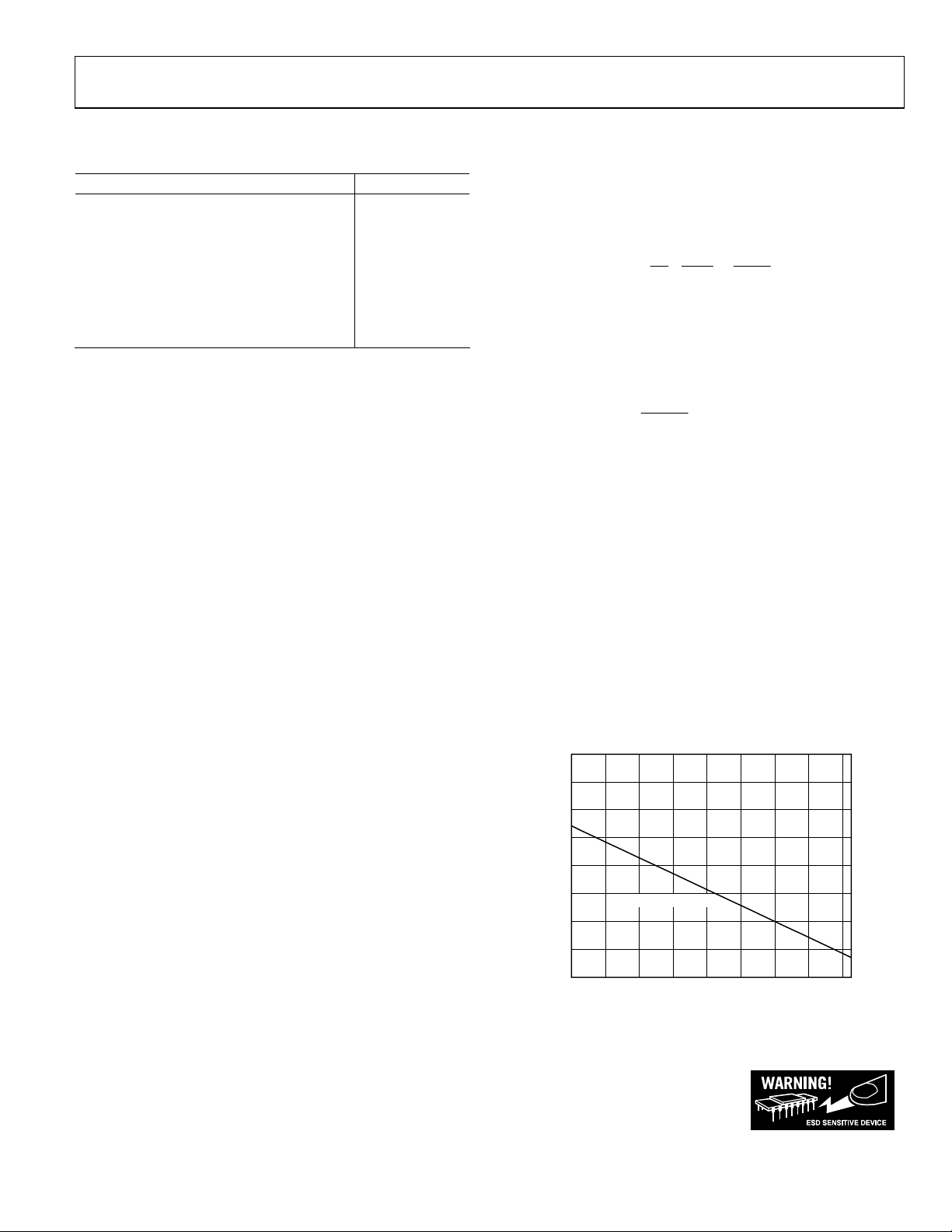
MAXIMUM POWER DISSIPATION
The maximum safe power dissipation in the AD8099 package is
limited by the associated rise in junction temperature (TJ) on
the die. The plastic encapsulating the die will locally reach the
junction temperature. At approximately 150°C, which is the
glass transition temperature, the plastic will change its
properties. Even temporarily exceeding this temperature limit
may change the stresses that the package exerts on the die,
permanently shifting the parametric performance of the
AD8099. Exceeding a junction temperature of 150°C for an
extended period can result in changes in silicon devices,
potentially causing failure.
× I
OUT
),
JA
).
The still-air thermal properties of the package and PCB (θ
the ambient temperature (T
the package (P
) determine the junction temperature of the die.
D
), and the total power dissipated in
A
The junction temperature can be calculated as
θPTT ×+=
J
The power dissipated in the package (
D
A
JA
P
) is the sum of the
D
quiescent power dissipation and the power dissipated in the
package due to the load drive for all outputs. The quiescent
V
power is the voltage between the supply pins (
I
quiescent current (
midsupply, the total drive power is
). Assuming the load (RL) is referenced to
S
V
/2 × I
S
dissipated in the package and some in the load (
) times the
S
, some of which is
OUT
V
OUT
Airflow will increase heat dissipation, effectively reducing θ
.
JA
Also, more metal directly in contact with the package leads
from metal traces, through holes, ground, and power planes will
reduce the θ
. Soldering the exposed paddle to the ground
JA
plane significantly reduces the overall thermal resistance of the
package. Care must be taken to minimize parasitic capacitances at the input leads of high speed op amps, as discussed in
the PCB Layout section.
Figure 4 shows the maximum safe power dissipation in the
package versus the ambient temperature for the exposed paddle
(e-pad) SOIC-8 (70°C/W), and CSP (70°C/W), packages on a
JEDEC standard 4-layer board. θ
4.0
3.5
3.0
2.5
2.0
1.5
1.0
0.5
MAXIMUM POWER DISSIPATION (Watts)
0.0
LFCSP AND SOIC
AMBIENT TEMPERATURE (°C)
Figure 4. Maximum Power Dissipation
values are approximations.
JA
120–40 –20 0 20 40 60 80 100
04511-0-115
ESD CAUTION
ESD (electrostatic discharge) sensitive device. Electrostatic charges as high as 4000 V readily accumulate on
the human body and test equipment and can discharge without detection. Although this product features
proprietary ESD protection circuitry, permanent damage may occur on devices subjected to high energy
electrostatic discharges. Therefore, proper ESD precautions are recommended to avoid performance
degradation or loss of functionality.
Rev. B | Page 5 of 28
Page 6
AD8099
TYPICAL PERFORMANCE CHARACTERISTICS
Default Conditions: VS = ±5 V, TA = 25°C, RL = 1 kΩ tied to ground unless otherwise noted. Refer to Figure 63 through Figure 66 for
component values and gain configurations.
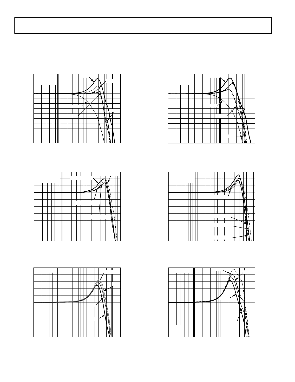
4
3
2
1
0
–1
–2
–3
–4
–5
–6
–7
–8
NORMALIZED CLOSED-LOOP GAIN (dB)
–9
–10
1
V
V
R
OUT
= ±5V
S
LOAD
= 0.2V p-p
= 1kΩ
10 100 1000
FREQUENCY (MHz)
G = +2
G = +5
G = +20
G = +10
G = –1
Figure 5. Small Signal Frequency Response for Various Gains (SOIC)
04511-0-074
4
3
2
1
0
–1
–2
–3
–4
–5
–6
–7
–8
NORMALIZED CLOSED-LOOP GAIN (dB)
–9
–10
1
V
V
R
OUT
S
LOAD
= 0.2V p-p
= ±5V
= 1kΩ
10 100 1000
G = +2
G = +20
G = –1
FREQUENCY (MHz)
G = +5
G = +10
Figure 8. Small Signal Frequency Response for Various Gains (CSP)
04511-0-073
17
G = +5
V
= ±5V
S
16
V
= 0.2V p-p
OUT
15
14
13
12
11
10
CLOSED-LOOP GAIN (dB)
9
8
7
1
RL = 100Ω, CSP
RL = 1kΩ, SOIC
10 100 1000
FREQUENCY (MHz)
RL = 1kΩ, CSP
RL = 100Ω, SOIC
04511-0-076
Figure 6. Small Signal Frequency Response for Various Load Resistors
11
V
= 0.2V p-p
OUT
10
9
8
7
6
5
4
CLOSED-LOOP GAIN (dB)
3
G = +2
2
= ±5V
V
S
R
= 1kΩ
L
1
FREQUENCY (MHz)
+25°C
+125°C
+85°C
–40°C
10001 10 100
04511-0-098
Figure 7. Small Signal Frequency Response for Various Temperatures (SOIC)
17
G = +5
R
= 1kΩ
L
16
V
= 0.2V p-p
OUT
15
14
13
12
11
10
CLOSED-LOOP GAIN (dB)
9
8
7
1
VS = ±5V, SOIC
VS = ±2.5V, CSP
VS = ±5V, CSP
VS = ±2.5V, SOIC
10 100 1000
FREQUENCY (MHz)
04511-0-077
Figure 9. Small Signal Frequency Response for Various Supply Voltages
11
V
= 0.2V p-p
OUT
10
9
8
7
6
5
4
CLOSED-LOOP GAIN (dB)
3
G = +2
2
V
= ±5V
S
= 1kΩ
R
L
1
FREQUENCY (MHz)
+125°C
–40°C
+25°C
+85°C
10001 10 100
04511-0-097
Figure 10. Small Signal Frequency Response for Various Temperatures (CSP)
Rev. B | Page 6 of 28
Page 7
AD8099
20
G = +5
VS = ±5V
19
18
17
16
15
14
13
12
CLOSED-LOOP GAIN (dB)
11
10
9
1
10 100 1000
FREQUENCY (MHz)
5pF, CSP
1pF, SOIC
1pF, CSP
5pF, SOIC
Figure 11. Small Signal Frequency Response for Various Capacitive Loads
1
0
–1
–2
–3
–4
–5
–6
–7
–8
VS = ±5V
V
= 2V p-p
–9
NORMALIZED CLOSED-LOOP GAIN (dB)
OUT
= 1k
LOAD
Ω
R
–10
1 10 100 1000
G = +2
G = +20
G = +5
FREQUENCY (MHz)
G = +10
04511-0-104
04511-0-011
90
80
70
60
50
40
30
20
OPEN-LOOP GAIN (dB)
10
VS = ±5V
0
= 1kΩ
R
L
UNCOMPENSATED
–10
0.001 0.01 0.1 1.0 10 100 1000
PHASE
FREQUENCY (MHz)
Figu nse
re 14. Open Loop Frequency Respo
MAGNITUDE
2
1
0
–1
–2
–3
–4
–5
–6
–7
VS = ±5V
= 2V p-p
V
–8
NORMALIZED CLOSED-LOOP GAIN (dB)
OUT
= 1k
LOAD
Ω
R
–9
1 10 100 1000
G = +2
G = +20
G = +5
FREQUENCY (MHz)
G = +10
–30
–45
–60
–75
–90
–105
–120
–135
–150
–165
–180
OPEN-LOOP PHASE (Degrees)
04511-0-012
04511-0-080
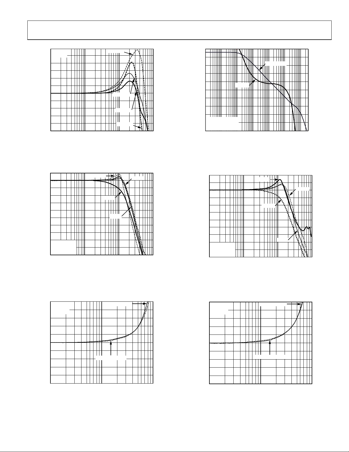
Figure 12. Large Signal Frequency Response for Various Gains (SOIC)
6.5
VS = ±5V
G = +2
6.4
= 150
Ω
R
L
6.3
6.2
6.1
6.0
5.9
5.8
CLOSED-LOOP GAIN (dB)
5.7
5.6
5.5
1
FREQUENCY (MHz)
V
= 1.4V p-p
OUT
V
= 200mV p-p
OUT
10 100
Figure 13. 0.1 dB latness (SOIC) F
04511-0-009
Rev. B | Page 7 of 28
Figure 15. Large Signal Frequency Response for Various Gains (CSP)
6.5
VS = ±5V
G = +2
6.4
= 150
Ω
R
L
6.3
6.2
6.1
6.0
5.9
5.8
CLOSED-LOOP GAIN (dB)
5.7
5.6
5.5
1
V
= 1.4V p-p
OUT
V
= 200mV p-p
OUT
10 100
FREQUENCY (MHz)
Figure 16. 0.1 d Flatness (CSP) B
04511-0-008
Page 8
AD8099
15
14
13
12
11
10
9
8
CLOSED-LOOP GAIN (dB)
7
G = +5
6
VS = ±5V
= 2V p-p
V
OUT
5
1
Figure 17. Large Sign us Load Resistances
RL = 100Ω, CSP
RL = 100Ω, SOIC
RL = 1kΩ, SOIC
10 100 1000
FREQUENCY (MHz)
al Frequency Response for Vario
100.0
10.0
RL = 1kΩ, CSP
04511-0-078
15
14
13
12
11
10
9
8
CLOSED-LOOP GAIN (dB)
7
G = +5
6
R
= 1k
Ω
L
V
= 2V p-p
OUT
5
1
Figu es
re 20. Large Signal Frequency Response for Various Supply Voltag
VS = ±2.5V, CSP
VS = ±5V, SOIC
VS = ±2.5V, SOIC
10 100 1000
FREQUENCY (MHz)
VS = ±5V, CSP
–10
G = +2
R
= 1kΩ
L
–20
V
= ±5V
S
V
= 0V
DIS
–30
04511-0-079
1.0
0.1
INPUT IMPEDANCE (kΩ)
0.01
VS = ±5V
G = +2
0.001
1
10 100 1000
Figure 18. Input Impedance vs. Frequency
100
10
)
Ω
1
0.1
OUTPUT IMPEDANCE (
VS = ±5V
0.01
Figure 19. Output Impedance . Frequency for Various Gains vs
FREQUENCY (MHz)
G = +2
FREQUENCY (MHz)
G = +5
G = +10
1000.1 1 10 1000
04511-0-105
04511-0-100
–40
–50
–60
OFF ISOLATION (dB)
–70
–80
–90
0.1
CSP
1 10 100 1000
FREQUENCY (MHz)
Figure 21. Off Isolation vs. Frequency
–50
G = +5
= 2V p-p
V
OUT
V
= ±5V
S
–60
= 100Ω
R
L
–70
–80
–90
–100
HARMONIC DISTORTION (dBc)
–110
–120
0.1 1.0 10.0
SOIC
SOLID LINES – SECOND HARMONICS
SOLID LINES – SECOND HARMONICS
DOTTED LINE – THIRD HARMONICS
FREQUENCY (MHz)
Figure 22. Harmonic D tion vs. Frequency istor
SOIC
CSP
04511-0-094
RMONICSDOTTED LINES– THIRD HA
04511-A-008
Rev. B | Page 8 of 28
Page 9
AD8099
–50
–60
–70
G = +5
V
OUT
V
= ±5V
S
R
= 1kΩ
L
= 2V p-p
–50
–60
–70
G = +5
V
OUT
V
= ±5V
S
R
= 1kΩ
L
= 2V p-p
–80
–90
–100
–110
HARMONIC DISTORTION (dBc)
–120
–130
0.1 1.0 10.0
Fig C)
ure 23. Harmonic Distortion vs. Frequency (SOI
SOLID LINE – SECOND HARMONIC
DOTTED LINE – THIRD HARMONIC
FREQUENCY (MHz)
–40
G = +2
V
= 2V p-p
OUT
–50
V
= ±5V
S
R
= 1kΩ
L
–60
–70
–80
–90
–100
–110
HARMONIC DISTORTION (dBc)
–120
–130
0.1 1.0 10.0
Figure 24. Harmonic Disto tion vs. Frequency (SOIC)
SOLID LINES – SECOND HARMONICS
SOLID LINE – SECOND HARMONIC
DOTTED LINE – THIRD HARMONICS
FREQUENCY (MHz)
r
–40
G = –1
= 2V p-p
V
OUT
–50
V
= ±5V
S
R
= 1kΩ
L
–60
–70
–80
–90
–100
–110
HARMONIC DISTORTION (dBc)
–120
–130
0.1 1.0 10.0
SOLID LINE – SECOND HARMONIC
DOTTED LINE – THIRD HARMONIC
FREQUENCY (MHz)
Figure 25. Harmonic Disto tion vs. Frequency (SOIC) r
–80
–90
–100
–110
HARMONIC DISTORTION (dBc)
–120
–130
0.1 1.0 10.0
04511-A-009
SOLID LINE – SECOND HARMONIC
DOTTED LINE – THIRD HARMONIC
FREQUENCY (MHz)
04511-A-012
Figure 26. Harmonic Distortion vs. Frequency (CSP)
–40
G = +2
V
= 2V p-p
OUT
–50
V
= ±5V
S
R
= 1kΩ
L
–60
–70
–80
–90
–100
–110
HARMONIC DISTORTION (dBc)
–120
CDOTTED LINE – THIRD HARMONI
04511-A-010
–130
0.1 1.0 10.0
SOLID LINE – SECOND HARMONIC
DOTTED LINE – THIRD HARMONIC
FREQUENCY (MHz)
04511-A-013
Figure 27. Harmonic Distortion vs. Frequency (CSP)
–40
G = –1
= 2V p-p
V
OUT
–50
V
= ±5V
S
R
= 1kΩ
L
–60
–70
–80
–90
–100
–110
HARMONIC DISTORTION (dBc)
–120
–130
04511-A-011
0.1 1.0 10.0
SOLID LINE – SECOND HARMONIC
DOTTED LINE – THIRD HARMONIC
FREQUENCY (MHz)
04511-A-014
Figure 28. Harmonic Distortion vs. Frequency (CSP)
Rev. B | Page 9 of 28
Page 10

AD8099
–50
G = +10
RL = 1kΩ
–60
–70
VS = ±2.5V
V
= 1V p-p
OUT
–50
–60
–70
G = +10
RL = 1kΩ
VS = ±2.5V
V
= 1V p-p
OUT
–80
–90
–100
HARMONIC DISTORTION (dBc)
–110
SOLID LINES – SECOND HARMONICS
–120
0.1 1.0 10.0
Figure 29. ge (SOIC)
Harmonic Distortion vs. Frequency and Supply Volta
DOTTED LINES – THIRD HARMONICS
FREQUENCY (MHz)
VS = ±5V
V
= 2V p-p
OUT
–40
G = +5
V
= ±5V
S
f = 10MHz
–50
R
= 100Ω
L
–60
–70
–80
–90
HARMONIC DISTORTION (dBc)
–100
SOLID LINE – SECOND HARMONIC
–110
DOTTED LINE – THIRD HARMONIC
7123456
OUTPUT AMPLITUDE (V p-p)
Figure 30. Harmonic Distortion vs. Output Amplitude (SOIC)
–40
G = +5
= ±5V
V
S
–50
f = 10MHz
R
= 1kΩ
L
–60
–80
–90
–100
HARMONIC DISTORTION (dBc)
–110
SOLID LINES – SECOND HARMONICS
SOLID LINES – SECOND HARMONICS
DOTTED LINE – THIRD HARMONICS
–120
0.1 1.0 10.0
04511-A-015
DOTTED LINES – THIRD HARMONICS
FREQUENCY (MHz)
VS = ±5V
V
= 2V p-p
OUT
04511-A-018
Figur CSP) e 32. Harmonic Distortion vs. Frequency for Various Supplies (
–40
G = +5
V
= ±5V
S
f = 10MHz
–50
R
= 100Ω
L
–60
–70
–80
–90
HARMONIC DISTORTION (dBc)
–100
SOLID LINE – SECOND HARMONIC
–110
04511-A-016
DOTTED LINE – THIRD HARMONIC
OUTPUT AMPLITUDE (V p-p)
7123456
04511-A-019
Figure 33. Harmonic Distortion vs. Output Amplitude (CSP)
–40
G = +5
= ±5V
V
S
–50
f = 10MHz
R
= 1kΩ
L
–60
–70
–80
–90
–100
HARMONIC DISTORTION (dBc)
–110
–120
SOLID LINE – SECOND HARMONIC
DOTTED LINE – THIRD HARMONIC
OUTPUT AMPLITUDE (V p-p)
Figure 31. Harmonic Distortion vs. Output Amplitude (SOIC)
7123456
04511-A-017
Rev. B | Page 10 of 28
–70
–80
–90
–100
HARMONIC DISTORTION (dBc)
–110
–120
SOLID LINE – SECOND HARMONIC
DOTTED LINE – THIRD HARMONIC
OUTPUT AMPLITUDE (V p-p)
Figure 34. Harmonic Distortion vs. Output Amplitude (CSP)
7123456
04511-A-021
Page 11

AD8099
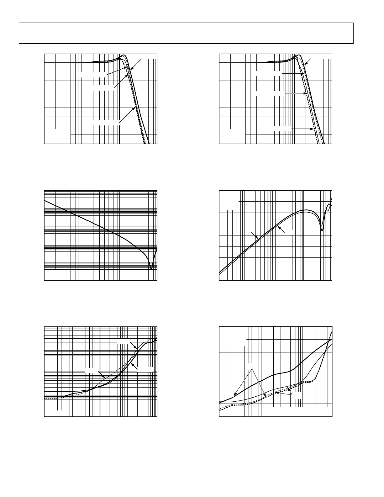
0.20
0.15
10pF, 20Ω R
SNUB
0.20
0.15
10pF, 20Ω R
SNUB
0.10
0.05
0
–0.05
OUTPUT VOLTAGE (V)
–0.10
–0.15
–0.20
Figur oads
e 35. Small Signal Transient Response for Various Capacitive L
G = +5
= ±5V
V
S
R
= 1kΩ
L
0510
1pF
R
SNUB
CLR
L
15 20 25 30 35 40 45 50
TIME (ns)
(SOIC)
0.15
0.10
0.05
0
–0.05
OUTPUT VOLTAGE (V)
–0.10
G = +10
R
= 1kΩ
L
–0.15
010
VS = ±5.0V
AND ±2.5V, CSP
VS = ±5.0V
AND ±2.5V, SOIC
20 30 40 50
TIME (ns)
t ResponFigure 36. Small Signal Transien se for Various Supply Voltages
OUTPUT VOLTAGE(V)
5
4
3
2
1
0
–1
–2
–3
–4
–5
RL = 100Ω
INPUT × 2
RL = 1kΩ
10000 100 200 300 400 500 600 700 800 900
TIME (ns)
04511-0-095
04511-0-107
04511-A-017
0.10
0.05
0
–0.05
OUTPUT VOLTAGE (V)
–0.10
–0.15
–0.20
0510
G = +5
= ±5V
V
S
R
= 1kΩ
L
1pF
R
SNUB
CLR
L
15 20 25 30 35 40 45 50
TIME (ns)
Figure 38. Small Signal Transient Response for Various Capacitive Loads
(CSP)
0.20
0.15
0.10
0.05
0
–0.05
OUTPUT VOLTAGE (V)
–0.10
RL = 1kΩ, 100Ω
–0.15
V
= 200mV p-p
OUT
G = +5
–0.20
010
VS = ±2.5V
CSP
VS = ±5.0V
SOIC
VS = ±2.5V
20 30 40 50
TIME (ns)
SOIC
VS = ±5.0V
CSP
Figure 39. Small Signal Transient Response for Various Supply Voltages
3.5
TURN OFF
INPUT
3.0
2.5
2.0
1.5
1.0
OUTPUT VOLTAGE (V)
0.5
TURN ON
0
–0.5
TIME (ns)
TURN ON
INPUT
VS = ±5V
TURN OFF
G = 2
2000 50 100 150
04511-0-096
04511-0-102
04511-0-010
Figure 37. Output Overdrive Rec very for Various Resistive Loads
o
Figure 40. Disable/Enable Switching Speed
Rev. B | Page 11 of 28
Page 12

AD8099
1.5
1.0
0.5
VS = ±2.5V
1.5
1.0
0.5
0.3%
OUTPUT
0.2%
INPUT
0.1%
0
–0.5
OUTPUT VOLTAGE (V)
–1.0
G = +10
= 1kΩ
R
L
–1.5
010
Figure 41. L ltage (CSP)
arge Signal Transient Response vs. Supply Vo
VS = ±5.0V
20 30 40 50
TIME (ns)
1.5
1.0
0.5
0
–0.5
OUTPUT VOLTAGE (V)
–1.0
G = +10
= 1kΩ
R
L
–1.5
010
VS = ±5.0V
VS = ±2.5V
20 30 40 50
TIME (ns)
F ) igure 42. Large Signal Frequency Response vs. Supply Voltage (SOIC
1.5
1.0
0.5
VS = ±5V
VS = ±2.5V
04511-0-106
04511-0-118
0
–0.5
OUTPUT/INPUT VOLTAGE (V)
–1.0
–1.5
0 5 10 15 20 25 30 35 40
Figu )
re 44. Short Term Settling Time (CSP
TIME (ns)
1.5
OUTPUT
1.0
0.5
0
–0.5
OUTPUT/INPUT VOLTAGE (V)
–1.0
–1.5
0 5 10 15 20 25 30 35 40
TIME (ns)
Figure 45. Short Term Settling Time (SOIC)
1.5
1.0
0.5
OUTPUT
INPUT
ERROR
INPUT
ERROR
G = +2
R
LOAD
V
= ±5V
s
G = +2
R
LOAD
V
= ±5V
s
= 1kΩ
= 1kΩ
G = +2
V
= ±5V
S
45
45
0%
–0.1%
–0.2%
–0.3%
0.3%
0.2%
0.1%
0%
–0.1%
–0.2%
–0.3%
0.30%
0.20%
0.10%
04511-0-052
04511-0-051
0
–0.5
OUTPUT VOLTAGE (V)
–1.0
RL = 1kΩ, 100Ω
G = +5
–1.5
010
Fig d
ure 43. Large Signal Transient Response for Various Supply Voltages an
Load Resistance (SOIC and CSP)
20 30 40 50
TIME (ns)
s
04511-0-101
Rev. B | Page 12 of 28
0
ERROR
–0.5
OUTPUT/INPUT VOLTAGE (V)
–1.0
–1.5
0 50 100 150 200 250 300 350 400 450
TIME (µs)
Figure 46. Long Term Settling Time
500
0%
–0.10%
–0.20%
–0.30%
04511-0-050
Page 13

AD8099
–20
G = +2
= 1kΩ
R
L
–30
–40
–50
–60
–70
–80
–90
COMMON-MODE REJECTION (dB)
–100
–110
FREQUENCY (MHz)
Figure 4 uen cy
7. Common-Mode Rej ection vs. Freq
1000
10000.1 1.0 10 100
04511-0-113
POWER SUPPLY REJECTION (dB)
0
G = +5
= 1kΩ
R
L
–10
–20
–30
–40
–50
–60
–70
–80
–90
–100
NEGATIVE
FREQUENCY (MHz)
Fi gure 50. Power Supply Rejection vs. Frequency
1000
POSITIVE
10000.01 0.10 1.0 10 100
04511-0-114
100
10
INPUT CURRENT NOISE (pA Hz)
1
1 10 100 1k 10k 100k 1M 10M 100M 1G
Figure 48. Input Current Noise v . Frequency (
1000
10
1
INPUT VOLTAGE NOISE (nV Hz)
0.1
1 10 100 1k 10k 100k 1M 10M 100M 1G
FREQUENCY (Hz)
s
FREQUENCY (Hz)
DISABLE
Figure 49. Input Voltage No ise vs. Frequency
= Open)
04511-0-004
04511-0-005
100
10
INPUT CURRENT NOISE (pA Hz)
1
1 10 100 1k 10k 100k 1M 10M 100M 1G
Figure 51. Input Current Noise vs. Frequency (
FREQUENCY (Hz)
DISABLE
120
100
80
60
COUNT
40
20
0
–300
–200 0–100 100 200
V
OFFSET
(µV)
Figure 52. Input Offset Voltage Distribution
= +VS)
VS = ±5V
N = 1,200
X
X = –70µV
σ
= 80µV
04511-0-003
04511-0-075
Rev. B | Page 13 of 28
Page 14

AD8099
400
20
V)
µ
OFFSET VOLTAGE (
300
200
100
–100
–200
0
VS = ±5V
TEMPERATURE (C)
VS =5V
F igure 53. Input Offset Voltage vs. Temperature
–5.4
IB+, VS = ±5V
IB+, VS =5V
A)
µ
BIAS CURRENT (
–5.6
–5.8
IB–, VS = ±5V
–6.0
–6.2
–6.4
–6.6
TEMPERATURE (C)
Figure 54. Input Bias Current vs. Temperature (
1.24
IB–, VS =5V
DISABLE
125–40 –25 –10 5 20 35 50 65 80 95 110
125–40 –25 –10 5 20 35 50 65 80 95 110
Pin Floating)
18
16
14
12
SUPPLY CURRENT (mA)
10
8
04511-A-003
VS = ±5V
VS =5V
TEMPERATURE (C)
125–40 –25 –10 5 20 35 50 65 80 95 110
04511-A-006
Figure 56. Supply Current vs. Temperature
1.0
0.8
0.6
0.4
A)
µ
0.2
IB–, VS = ±5V
0
–0.2
–0.4
BIAS CURRENT (
–0.6
–0.8
–1.0
04511-A-004
Figure 57. Input Bias Current vs. Temperature (
IB+, VS = ±5V
IB–, VS =5V
TEMPERATURE (C)
IB+, VS =5V
DISABLE
125–40 –25 –10 5 20 35 50 65 80 95 110
Pin = +VS)
04511-A-007
–VS +V
1.22
VS = ±5V
1.20
1.18
–VS +V
1.16
1.14
OUTPUT SATURATION VOLTAGE (V)
1.12
OUT
VS =5V
OUT
+VS–V
+VS–V
TEMPERATURE (C)
Figure 55. Output Saturation Voltage vs. Temperature
OUT
OUT
125–40–25–10–5203550658095110
04511-A-005
Rev. B | Page 14 of 28
Page 15

AD8099
THEORY OF OPERATION
The AD8099 is a voltage feedback op amp that employs a new
highly linear low noise input stage. With this input stage, the
AD8099 can achieve better than 90 dB distortion for a 2 V p-p,
10 MHz output signal with an input referred voltage noise of
less than 1 nV/√
. This noise level and distortion
Hz
performance has been previously achievable only with fully
uncompensated amplifiers. The AD8099 achieves this level of
performance for gains as low as +2. This new input stage also
triples the achievable slew rate for comparably compensated 1
nV/√
amplifiers.
Hz
The simplified AD8099 topology is shown in Figure 58. The
amplifier is a single gain stage with a unity gain output buffer
fabricated in Analog Devices’ extra fast complimentary bipolar
process (XFCB). The AD8099 has 85 dB of open-loop gain and
maintains precision specifications such as CMRR, PSRR, VOS,
and ∆V
/∆T to levels that are normally associated with
OS
topologies having two or more gain stages.
R1 R
Figure 58. AD8099 Topology
BUFFERgm
C
C
V
OUT
L
04511-0-060
The AD8099 can be externally compensated down to a gain of 2
through the use of an RC network. Above gains of 15, no external compensation network is required. To realize the full gain
bandwidth product of the AD8099, no PCB trace should be
connected to or within close proximity of the external compensation pin for the lowest possible capacitance.
External compensation allows the user to optimize the closedloop response for minimal peaking while increasing the gain
bandwidth product in higher gains, lowering distortion errors
that are normally more prominent with internally compensated
parts in higher gains. For a fixed gain bandwidth, wideband
distortion products would normally increase by 6 dB going
from a closed-loop gain of 2 to 4. Increasing the gain bandwidth
product of the AD8099 eliminates this effect with increasing
closed-loop gain.
The AD8099 is available in both a SOIC and an LFCSP, each of
which has a thermal pad for lower operating temperature. To
help avoid this pad in board layout, both packages have an extra
output pin on the opposite side of the package for ease in connecting a feedback network to the inputs. The secondary output
pin also isolates the interaction of any capacitive load on the
output and self-inductance of the package and bond wire from
the feedback loop. While using the secondary output for feedback, inductance in the primary output will now help to isolate
capacitive loads from the output impedance of the amplifier.
Since the SOIC has greater inductance in its output, the SOIC
will drive capacitive loads better than the LFCSP. Using the
primary output for feedback with both packages will result in
the LFCSP driving capacitive load better than the SOIC.
The LFCSP and SOIC pinouts are identical, except for the
rotation of all pins counterclockwise by one pin on the LFCSP.
This isolates the inputs from the negative power supply pin,
removing a mutually inductive coupling that is most prominent
while driving heavy loads. For this reason, the LFCSP second
harmonic, while driving a heavy load, is significantly better
than that of the SOIC.
A three-state input pin is provided on the AD8099 for a high
impedance power-down and an optional input bias current
cancellation circuit. The high impedance output allows several
AD8099s to drive the same ADC or output line time interleaved. Pulling the
DISABLE
pin low activates the high
impedance state. See Table 5 for threshold levels. When the
DISABLE
With the
pin is left floating, the AD8099 operates normally.
DISABLE
pin pulled within 0.7 V of the positive
supply, an optional input bias current cancellation circuit is
turned on, which lowers the input bias current to less than 200
nA. In this mode, the user can drive the AD8099 with a high dc
source impedance and still maintain minimal output referred
offset without having to use impedance matching techniques. In
addition, the AD8099 can be ac-coupled while setting the bias
point on the input with a high dc impedance network. The
input bias current cancellation circuit will double the input
referred current noise, but this effect is minimal as long as
wideband impedance is kept low (see Figure 48 and Figure 51).
A pair of internally connected diodes limits the differential
voltage between the noninverting input and the inverting input
of the AD8099. Each set of diodes has two series diodes, which
are connected in anti-parallel. This limits the differential
voltage between the inputs to approximately ±1.8 V. All of the
AD8099 pins are ESD protected with voltage limiting diodes
connected between both rails. The protection diodes can handle
5 mA of steady state current. Currents should be limited to 5
mA or less through the use of a series limiting resistor.
Rev. B | Page 15 of 28
Page 16

AD8099
APPLICATIONS
USING THE AD8099
The AD8099 offers unrivaled noise and distortion performance
in low signal gain configurations. In low gain configurations
(less than15), the AD8099 requires external compensation. The
amount of gain and performance needed will determine the
compensation network.
Understanding the subtleties of the AD8099 gives the user
insight on how to exact its peak performance. Use the
component values and circuit configurations shown in the
Applications section as starting points for designs. Specific
circuit applications will dictate the final configuration and value
of your components.
CIRCUIT COMPONENTS
The circuit components are referenced in Figure 59, the
recommended noninverting circuit schematic for the AD8099.
See Table 4 for typical component values and performance data.
C
F
+V
S
C2
10µF
R
F
R
G
2
R
V
IN
Figure 59. Wideband Noninverting Gain Configuration (SOIC)
RF and R
G
S
R1
DISABLE
—The feedback resistor and the gain set resistor
AD8099
3
8
C5
0.1µF
C4
10µF
determine the noise gain of the amplifier; typical R
range from 250 Ω to 499 Ω.
C3
0.1µF
1
7
6
5
4
R
C
C
C
–V
S
V
OUT
C1
04511-0-061
values
F
C
—Creates a zero in the loop response to compensate the pole
F
created by the input capacitance (including stray capacitance)
and the feedback resistor R
. CF helps reduce high frequency
F
peaking and ringing in the closed-loop response. Typical range
is 0.5 pF to 1.5 pF for evaluation circuits used here.
R1—This resistor terminates the input of the amplifier to the
source resistance of the signal source, typically 50 Ω. (This is
application specific and not always required.)
R
—Many high speed amplifiers in low gain configurations
S
require that the input stage be terminated into a nominal
impedance to maintain stability. The value of R
should be kept
S
to 50 Ω or lower to maintain low noise performance. At higher
gains, R
may be reduced or even eliminated. Typical range is
S
0 Ω to 50 Ω.
C
—The compensation capacitor decreases the open-loop gain
C
at higher frequencies where the phase is degrading. By decreasing the open-loop gain here, the phase margin is increased and
the amplifier is stabilized. Typical range is 0 pF to 5 pF. The
value of C
is gain dependent.
C
RC—The series lead inductance of the package and the com-
pensation capacitance (CC) forms a series resonant circuit. RC
dampens this resonance and prevents oscillations. The
recommended value of R
is 50 Ω for a closed-loop gain of 2.
C
This resistor introduces a zero in the open-loop response and
must be kept low so that this zero occurs at a higher frequency.
The purpose of the compensation network is to decrease the
open-loop gain. If the resistance becomes too large, the gain will
be reduced to the resistor value, and not necessarily to 0 Ω,
which is what a single capacitor would do over frequency.
Typical value range is 0 Ω to 50 Ω.
C1—To lower the impedance of R
R
. C1 is not required, but greatly reduces peaking at low
C
, C1 is placed in parallel with
C
closed-loop gains. The typical value range is 0 pF to 2 pF.
C2 and C3—Bypass capacitors are connected between both
supplies for optimum distortion and PSRR performance. These
capacitors should be placed as close as possible to the supply
pins of the amplifier. For
C3, C5, a 0508 case size should be
used. The 0508 case size offers reduced inductance and better
frequency response.
C4 and C2—Electrolytic bypass capacitors.
Rev. B | Page 16 of 28
Page 17

AD8099
V
V
RECOMMENDED VALUES
Table 4. Recommended Values and AD8099 Performance
Feedback
Network Values
Gain Package
R
FRGRSCFRC
−1, 2 SOIC 250 250 50 1.5 50 4 1.5 440/700 515 0.3/3.1 2.1 4
2 CSP 250 250 50 0.5 50 5 2 700 475 3.2 2.1 4
−1 CSP 250 250 50 1.0 50 5 2 420 475 0.8 2.1 4
5 CSP/SOIC 499 124 20 0.5 50 1 0 510 735 1.4 4.9 8.6
10 CSP/SOIC 499 54 0 0 0 0.5 0 550 1350 0.8 9.6 13.3
20 CSP/SOIC 499 26 0 0 0 0 0 160 1450 0 19 23.3
CIRCUIT CONFIGURATIONS
Figure 60 through Figure 66 show typical schematics for the
AD8099 in various gain configurations. Table 4 data was
collected using the schematics shown in Figure 60 through
Figure 66. Resistor R1, as shown in Figure 60 through Figure 66,
C
F
1.5pF
250Ω
R
G
IN
R1
50Ω
250Ω
R
S
50Ω
DISABLE
R
F
1
2
AD8099
3
8
C5
0.1µF
C4
10µF
+V
7
4
Compensation
Network Values
S
C2
10µF
C3
0.1µF
6
5
R
C
50Ω
C
C
4pF
C1
1.5pF
−3 dB SS
Bandwidth
C
C1
C
(MHz)
Slew Rate
(V/µs)
Peaking
(dB)
Output Noise
(AD8099 Only)
(nV/√
Hz
)
Total Output Noise
Including Resistors
(nV/√Hz)
is the test equipment termination resistor. R1 is not required for
normal operation, but is shown in the schematics for
completeness.
C
F
1pF
+V
S
C2
10µF
C3
0.1µF
2
8
7
6
5
R
C
C1
50Ω
2pF
C
C
5pF
RL
1kΩ
V
OUT
R
1kΩ
R
F
250Ω
R
G
R1
50Ω
250Ω
R
S
50Ω
DISABLE
3
AD8099
4
1
C5
0.1µF
C4
10µF
V
IN
V
OUT
L
–V
S
Figure 60. Amplifier Configuration for SOIC Package, Gain = –1
C
F
1.5pF
250Ω
R
G
250Ω
R
S
IN
50Ω
R1
50Ω
DISABLE
R
F
2
AD8099
3
8
C5
0.1µF
C4
10µF
+V
S
C2
10µF
C3
0.1µF
1
7
6
5
4
C1
R
C
1.5pF
50Ω
C
C
4pF
–V
S
R
1kΩ
V
OUT
L
Figure 61. Amplifier Configuration for SOIC Package, Gain = +2
04511-0-116
04511-0-054
Rev. B | Page 17 of 28
–V
S
Figure 62. Amplifier Configuration for CSP Package, Gain =–1
C
F
0.5pF
250Ω
R
G
250Ω
R
S
V
IN
50Ω
R1
50Ω
DISABLE
R
F
2
3
AD8099
4
1
C5
0.1µF
C4
10µF
+V
S
C2
10µF
C3
0.1µF
8
7
6
5
C1
R
C
2pF
50Ω
C
C
5pF
–V
S
R
1kΩ
V
OUT
L
Figure 63. Amplifier Configuration for CSP Package, Gain = +2
04511-0-108
04511-0-053
Page 18

AD8099
V
V
V
C
F
0.5pF
499Ω
R
G
124Ω
R
S
20Ω
IN
R1
50Ω
DISABLE
Figure 64. Amplifier Configuration for CSP and SOIC Package, Gain = +5
499Ω
R
G
54Ω
IN
R1
50Ω
DISABLE
R
F
FB
–
AD8099
+
D
C5
0.1µF
C4
10µF
R
F
FB
–
AD8099
+
D
C5
0.1µF
C4
10µF
+V
S
C2
10µF
C3
0.1µF
+V
V
O
C
C
–V
R
C
50Ω
C
C
1pF
–V
S
R
1kΩ
V
OUT
L
+V
S
C2
10µF
C3
0.1µF
+V
V
O
C
C
–V
C
C
0.5pF
R
1kΩ
V
OUT
L
04511-0-055
+V
S
C2
R
F
499Ω
R
G
26Ω
–
AD8099
IN
R1
50Ω
DISABLE
+
0.1µF
C5
C4
10µF
D
10µF
C3
0.1µF
FB
+V
V
O
C
C
–V
–V
S
R
1kΩ
V
OUT
L
04511-0-057
Figure 66. Amplifier Configuration for CSP and SOIC Packages, Gain = +20
–V
S
04511-0-056
Figure 65. Amplifier Configuration for CSP and SOIC Packages, Gain = +10
Rev. B | Page 18 of 28
Page 19

AD8099
T
V
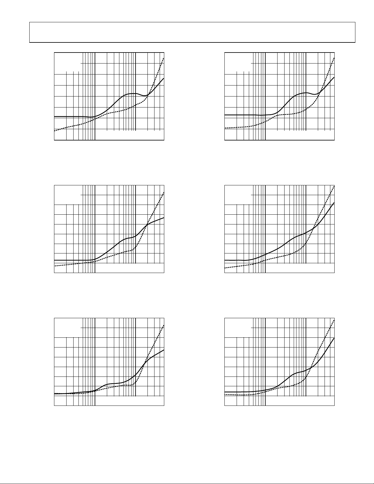
PERFORMANCE VS. COMPONENT VALUES
The influence that each component has on the AD8099
frequency response can be seen in Figure 67 and Figure 68. In
Figure 67 and Figure 68, all component values are held
constant, except for the individual component shown, which is
varied. For example, in the R
components are held constant except R
0 Ω to 50 Ω.; and clearly indicates that R
on peaking and bandwidth of the AD8099.
IN
R1
SOIC PINOUT SHOWN
10
VS = ±5V
G = +2
9
R
= 1kΩ
LOAD
SOIC PACKAGE
8
7
6
5
4
3
2
CLOSED-LOOP GAIN (dB)
1
0
–1
1 10 100 1000
performance plot of Figure 68, all
S
, which is varied from
S
has a major influence
S
C
F
+V
S
C2
10µF
R
R
G
R
S
DISABLE
F
2
AD8099
3
8
C5
0.1µF
C4
10µF
FREQUENCY (MHz)
C3
0.1µF
1
7
6
5
4
R
C
C
C
–V
S
CC = 5pF
Figure 67. Frequency Response for Various Values of C1, C
C1
V
04511-0-117
CC = 3pF
CC = 4pF
OU
3000
04511-0-024
9
8
7
6
5
4
3
2
1
CLOSED-LOOP GAIN (dB)
VS = ±5V
0
G = +2
–1
R
= 1kΩ
LOAD
SOIC PACKAGE
–2
1 10 100 1000
10
VS = ±5V
G = +2
9
= 1k
R
LOAD
SOIC PACKAGE
8
7
6
5
4
3
2
CLOSED-LOOP GAIN (dB)
1
0
–1
1
FREQUENCY (MHz)
Ω
10 100 1000
FREQUENCY (MHz)
, R
C
C
C1 = 1.5pF
RC = 20
RC = 35
C1 = 2pF
Ω
Ω
C1 = 0pF
RC = 50
3000
Ω
3000
04511-0-020
04511-0-030
Rev. B | Page 19 of 28
Page 20

AD8099
T
V
CLOSED-LOOP GAIN (dB)
CLOSED-LOOP GAIN (dB)
10
9
8
7
6
5
4
3
2
1
VS = ±5V
G = +2
0
R
LOAD
SOIC PACKAGE
–1
1
12
11
10
9
8
7
6
5
4
3
VS = ±5V
2
G = +2
1
R
LOAD
SOIC PACKAGE
0
1
RF = RG = 300
RF = RG = 250
= 1k
Ω
10 100 1000
FREQUENCY (MHz)
= 1kΩ
10 100 1000
FREQUENCY (MHz)
RF = RG = 200
3000
04511-0-032
RS = 0
RS = 50
RS = 20
10000
04511-0-034
10
9
8
7
6
5
4
3
2
CLOSED-LOOP GAIN (dB)
1
V = ±5V
S
G = +2
0
R
LOAD
SOIC PACKAGE
–1
1
IN
SOIC PINOUT SHOWN
Figure 68. Frequency Response for Various Values of R
= 1kΩ
R1
DISABLE
10
R
G
R
S
, CF, R
F
CF = 0.5pF
CF = 1pF
CF = 1.5pF
FREQUENCY (MHz)
C
R
2
3
0.1µF
S
100 1000 3000
F
+V
S
F
1
7
AD8099
10µF
5
4
8
C5
C4
–V
S
C2
10µF
C3
0.1µF
6
R
C
C
C
04511-0-058
V
OU
C1
04511-0-117
TOTAL OUTPUT NOISE CALCULATIONS AND DESIGN
To analyze the noise performance of an amplifier circuit, the
individual noise sources must be identified. Then determine if
the source has a significant contribution to overall noise performance of the amplifier. To simplify the noise calculations, we
will work with noise spectral densities, rather than actual
voltages to leave bandwidth out of the expressions (noise
spectral density, which is generally expressed in nV/√
equivalent to the noise in a 1 Hz bandwidth).
The noise model shown in Figure 69 has six individual noise
sources: the Johnson noise of the three resistors, the op amp
voltage noise, and the current noise in each input of the
amplifier. Each noise source has its own contribution to the
, is
Hz
Rev. B | Page 20 of 28
noise at the output. Noise is generally specified RTI (referred to
input), but it is often simpler to calculate the noise referred to
the output (RTO) and then divide by the noise gain to obtain
the RTI noise.
All resistors have a Johnson noise of √
–23
Boltzmann’s Constant (1.38 × 10
J/K), T is the absolute
(4kBTR)
, where k is
temperature in Kelvin, B is the bandwidth in Hz, and R is the
resistance in ohms. A simple relationship, which is easy to
remember, is that a 50 Ω resistor generates a Johnson noise of
1 nV√
at 25°C. The AD8099 amplifier has roughly the same
Hz
equivalent noise as a 50 Ω resistor.
Page 21

AD8099
V
N, R1
B
4kTR1
V
N, R3
A
4kTR3
RTI NOISE =
RTO NOISE = NG × RTI NOISE
I
R1
R3
I
N–
N+
2
V
N
+
I
N+
V
N, R2
4kTR2
V
N
+ 4kTR3 + 4kTR1
2
R32 + I
R1 × R2
2
N–
R1 + R2 R1 + R2
R2
"B" TO OUTPUT
R2
R1 + R2
GAIN FROM
"A" TO OUTPUT
NOISE GAIN =
V
OUT
GAIN FROM
2
2
+ 4kTR2
NG = 1 +
=–
R1
=
R2
R1
R2
R1
2
04511-0-070
Figure 69. Op Amp Noise Analysis Model
In applications where noise sensitivity is critical, care must be
taken not to introduce other significant noise sources to the
amplifier. Each resistor is a noise source. Attention to the
following areas is critical to maintain low noise performance:
design, layout, and component selection. A summary of noise
performance for the amplifier and associated resistors can be
seen in Table 4.
INPUT BIAS CURRENT AND DC OFFSET
In high noise gain configurations, the effects of output offset
voltage can be significant, even with low input bias currents and
input offset voltages. Figure 70 shows a comprehensive offset
voltage model, which can be used to determine the referred to
output (RTO) offset voltage of the amplifier or referred to input
(RTI) offset voltage.
R2
I
B
R1
A
R3
B–
V
OS
I
B+
GAIN FROM
"A" TO OUTPUT
NOISE GAIN =
NG = 1 +
V
OUT
GAIN FROM
"B" TO OUTPUT
=–
=
R2
R1
R2
R1
For RTO calculations, the input offset voltage and the voltage
generated by the bias current flowing through R3 are multiplied
by the noise gain of the amplifier. The voltage generated by I
B–
through R2 is summed together with the previous offset
voltages to arrive at a final output offset voltage. The offset
voltage can also be referred to the input (RTI) by dividing the
calculated output offset voltage by the noise gain.
As seen in Figure 70 if I
and IB– are the same and R3 equals the
B+
parallel combination of R1 and R2, then the RTI offset voltage
can be reduced to only V
This is a common method used to
OS.
reduce output offset voltage. Keeping resistances low helps to
minimize offset error voltage and keeps the voltage noise low.
DISABLE
The AD8099
PIN AND INPUT BIAS CANCELLATION
DISABLE
pin performs three functions; enable,
disable, and reduction of the input bias current. When the
DISABLE
pin is brought to within 0.7 V of the positive supply,
the input bias current is reduced by an approximate factor of 60.
However, the input current noise doubles to 5.2 pA/√
5 outlines the
Table 5.
DISABLE
DISABLE
pin functionality.
Pin Truth Table
Hz
. Table
Supply Voltage ±5 V +5 V
Disable –5 to +2.4 0 to 2.4
Enable Open Open
Low Input Bias Current 4.3 to 5 4.3 to 5
OFFSET (RTO) = VOS 1 +R2 + IB+× R3 1 +R2– IB–× R2
OFFSET (RTI) = VOS + IB+× R3 – I
FOR BIAS CURRENT CANCELLATION:
OFFSET (RTI) = VOS IF IB+ = IB– AND R3 =
R1 R1
R1 × R2
B–
R1 + R2
R1 + R2
R1 × R2
Figure 70. Op Amp Total Offset Voltage Model
04511-0-071
Rev. B | Page 21 of 28
Page 22

AD8099
+V
S
C1
10µF
C2
0.1µF
C1
2pF
R7
15Ω
7
6
5
4
R
C
50Ω
C
C
9pF
–V
S
V
IN
+2.5V
R1
590ΩR2590Ω
R
G
150Ω
R
S
50Ω
DISABLE
R
F
150Ω
2
AD8099
3
C4
10µF
C5
0.1µF
1
8
Figure 71. ADC Driver
16-BIT ADC DRIVER
Ultralow noise and distortion performance make the AD8099
an ideal ADC driver. Even though the AD8099 is not unity gain
stable, it can be configured to produce a net gain of +1
amplifier, as shown in Figure 71. This is achieved by combining
a gain of +2 and a gain of –1 for a net gain of +1. The input
range of the ADC is 0 V to 2.5 V.
Table 6 shows the performance data of the AD8099 and the
Analog Devices
AD7667 a 1 MSPS 16-bit ADC.
REF
1µF
C6
2.7nF
DVDD
47µF
AVDD
0.1µF
AGND AVDD DGND DVDD
REF
0.1µF
AD7667
REFGND
IN
INGND
04511-0-072
Table 6. ADC Driver Performance, fC = 20 kHz,
= 2.24 V p-p
V
OUT
Parameter Measurement (dB)
Second Harmonic Distortion –111.4
Third Harmonic Distortion –103.2
THD –101.4
SFDR 102.2
SNR 88.1
Rev. B | Page 22 of 28
Page 23

AD8099
CIRCUIT CONSIDERATIONS
Optimizing the performance of the AD8099 requires attention
to detail in layout and signal routing of the board. Power supply
bypassing, parasitic capacitance, and component selection all
contribute to the overall performance of the amplifier. The
AD8099 features an exposed paddle on the backs of both the
CSP and SOIC packages. The exposed paddle provides a low
thermal resistive path to the ground plane. For best
performance, solder the exposed paddle to the ground plane.
PCB Layout
The compensation network is determined by the amplifier gain
requirements. For lower gains, the layout and component
placement are more critical. For higher gains, there are fewer
compensation components, which results in a less complex
layout. With diligent consideration to layout, grounding, and
component placement, the AD8099 evaluation boards have
been optimized for peak performance. These are the same
evaluation boards that are available to customers; see Table 7 for
ordering information. The noninverting evaluation board artwork for SOIC and CSP layouts are shown in Figure 72 and
Figure 73. Incorporating the layout information shown in
Figure 72 and Figure 73 into new designs is highly recommended and helps to ensure optimal circuit performance. The
concepts of layout, grounding, and component placement,
llustrated in Figure 72 and Figure 73,also apply to inverting
configurations. For scale, the boards are 2” × 2”.
Parasitics
The area surrounding the compensation pin is very sensitive to
parasitic capacitance. To realize the full gain bandwidth product
of the AD8099, there should be no trace connected to or within
close proximity of the external compensation pin for the lowest
possible capacitance. When compensation is required, the
traces to the compensation pin, the negative supply, and the
interconnect between components (i.e. C
59) should be made as wide as possible to minimize inductance.
All ground and power planes under the pins of the AD8099
should be cleared of copper to prevent parasitic capacitance
between the input and output pins to ground. A single mounting pad on a SOIC footprint can add as much as 0.2 pF of
capacitance to ground as a result of not clearing the ground or
power plane under the AD8099 pins. Parasitic capacitance can
cause peaking and instability, and should be minimized to
ensure proper operation.
The new pinout of the AD8099 reduces the distance between
the output and the inverting input of the amplifier. This helps to
minimize the parasitic inductance and capacitance of the
feedback path, which, in turn, reduces ringing and second
harmonic distortion.
, C1, and RC in Figure
C
Grounding
When possible, ground and power planes should be used.
Ground and power planes reduce the resistance and inductance
of the power supply feeds and ground returns. If multiple planes
are used, they should be “stitched” together with multiple vias.
The returns for the input, output terminations, bypass
capacitors, and R
should all be kept as close to the AD8099 as
G
possible. Ground vias should be placed at the very end of the
component mounting pad to provide a solid ground return. The
output load ground and the bypass capacitor grounds should be
returned to a common point on the ground plane to minimize
parasitic inductance and improve distortion performance. The
AD8099 packages feature an exposed paddle. For optimum
performance, solder this paddle to ground. For more
information on PCB layout and design considerations, refer to
section 7-2 of the 2002 Analog Devices Op Amp Applications
book.
Power Supply Bypassing
The AD8099 power supply bypassing has been optimized for
each gain configuration as shown in Figure 60 through
Figure 66 in the Circuit Configurations section. The values
shown should be used when possible. Bypassing is critical for
stability, frequency response, distortion, and PSRR
performance. The 0.1 µF capacitors shown in Figure 60 through
Figure 66 should be as close to the supply pins of the AD8099 as
possible and the electrolytic capacitors beside them.
Component Selection
Smaller components less than 1206 SMT case size, offer smaller
mounting pads, which have less parasitics and allow for a more
compact layout. It is critical for optimum performance that high
quality, tight tolerance (where critical), and low drift components be used. For example, tight tolerance and low drift is
critical in the selection of the feedback capacitor used in
Figure 60. The feedback compensation capacitor in Figure 60 is
1.5pF. This capacitor should be specified with NPO material.
NPO material typically has a ±30 ppm/°C change over –55°C to
+125°C temperature range. For a 100°C change, this would
result in a 4.5 fF change in capacitance, compared to an X7R
material, which would result in a 0.23 pF change, a 15% change
from the nominal value. This could introduce excessive
peaking, as shown in Figure 68, C
vs. Frequency Response.
F
DESIGN TOOLS AND TECHNICAL SUPPORT
Analog Devices is committed to the design process by providing
technical support and online design tools. ADI offers technical
support via free evaluation boards, sample ICs, SPICE models,
interactive evaluation tools, application notes, phone and email
support—all available at
www.analog.com.
Rev. B | Page 23 of 28
Page 24

AD8099
Figure 72. SOIC Evaluation Board Artwork
04511-A-001
04511-A-001
Figure 73. CSP Evaluation Board Artwork
Evaluation Boards
There are four different evaluation boards available, as shown in Table 7, and an Application Note, AN-720, that explains the use of the
evaluation boards.
Table 7. Evaluation Board Selection Guide
Package Type
Board Configuration
CSP SOIC
Inverting EVAL-ADOPAMP-1CSP-I EVAL-ADOPAMP-1R-IN
Noninverting EVAL-ADOPAMP-1CSP-N EVAL-ADOPAMP-1R-NI
Rev. B | Page 24 of 28
Page 25

AD8099
Y
OUTLINE DIMENSIONS
4.00 (0.157)
3.90 (0.154)
3.80 (0.150)
5.00 (0.197)
4.90 (0.193)
4.80 (0.189)
85
TOP VIEW
41
6.20 (0.244)
6.00 (0.236)
5.80 (0.228)
BOTTOM VIEW
(PINS UP)
2.29 (0.092)
2.29 (0.092)
1.27 (0.05)
BSC
0.25 (0.0098)
0.10 (0.0039)
COPLANARIT
0.10
CONTROLLING DIMENSIONS ARE IN MILLIMETERS; INCH DIMENSIONS
(IN PARENTHESES) ARE ROUNDED-OFF MILLIMETER EQUIVALENTS FOR
REFERENCE ONLY AND ARE NOT APPROPRIATE FOR USE IN DESIGN
SEATING
PLANE
COMPLIANT TO JEDEC STANDARDS MS-012
1.75 (0.069)
1.35 (0.053)
0.51 (0.020)
0.31 (0.012)
0.25 (0.0098)
0.17 (0.0068)
0.50 (0.020)
0.25 (0.010)
8°
1.27 (0.050)
0°
0.40 (0.016)
Figure 74. 8-Lead Standard Small Outline Package [SOIC-ED]
(RD-8-1)
0.50
0.40
PIN 1
INDICATOR
0.90
0.85
0.80
SEATING
PLANE
12° MAX
3.00
BSC SQ
TOP
VIEW
0.30
0.23
0.18
0.80 MAX
0.65TYP
2.75
BSC SQ
0.20 REF
0.05 MAX
0.02 NOM
0.45
0.50
BSC
0.60 MAX
0.25
MIN
8
5
BOTTOM
VIEW
0.30
4
1
1.60
1.45
1.30
Figure 75. 8-Lead Plastic Surface-Mount Package [CSP]
(CP-8)
Dimensions shown in millimeters
1.50
REF
× 45°
PIN 1
INDICATOR
1.90
1.75
1.60
Rev. B | Page 25 of 28
Page 26

AD8099
ORDERING GUIDE
Model Minimum Ordering Quantity Temperature Range Package Description Branding Package Option
AD8099ARD 1 –40°C to +125°C 8-Lead SOIC-ED RD-8-1
AD8099ARD-REEL 2,500 –40°C to +125°C 8-Lead SOIC-ED RD-8-1
AD8099ARD-REEL7 1,000 –40°C to +125°C 8-Lead SOIC-ED RD-8-1
AD8099ARDZ
AD8099ARDZ-REEL1 2,500 –40°C to +125°C 8-Lead SOIC-ED RD-8-1
AD8099ARDZ-REEL71 1,000 –40°C to +125°C 8-Lead SOIC-ED RD-8-1
AD8099ACP-R2 250 –40°C to +125°C 8-Lead CSP HDB CP-8
AD8099ACP-REEL 5,000 –40°C to +125°C 8-Lead CSP HDB CP-8
AD8099ACP-REEL7 1,500 –40°C to +125°C 8-Lead CSP HDB CP-8
AD8099ACPZ-R21 250 –40°C to +125°C 8-Lead CSP HDB CP-8
AD8099ACPZ-REEL1 5,000 –40°C to +125°C 8-Lead CSP HDB CP-8
AD8099ACPZ-REEL71 1,500 –40°C to +125°C 8-Lead CSP HDB CP-8
1
1 –40°C to +125°C 8-Lead SOIC-ED RD-8-1
1
Z = Pb free
Rev. B | Page 26 of 28
Page 27

AD8099
NOTES
Rev. B | Page 27 of 28
Page 28

AD8099
NOTES
© 2004 Analog Devices, Inc. All rights reserved. Trademarks and
registered trademarks are the property of their respective owners.
D04511–0–6/04(B)
Rev. B | Page 28 of 28
 Loading...