

Datasheet AD8072JR, AD8072JN, AD8072ARM-REEL7, AD8072ARM-REEL, AD8072ARM Datasheet (Analog Devices)
...Page 1
Low Cost, Dual/Triple
(
)
TOP VIEW
(Not to Scale)
14
13
12
11
10
9
8
1
2
3
4
5
6
7
NC = NO CONNECT
NC
NC
+V
S
+IN1
–IN1
OUT1
OUT2
–IN2
+IN2
–V
S
+IN3
–IN3
OUT3
NC
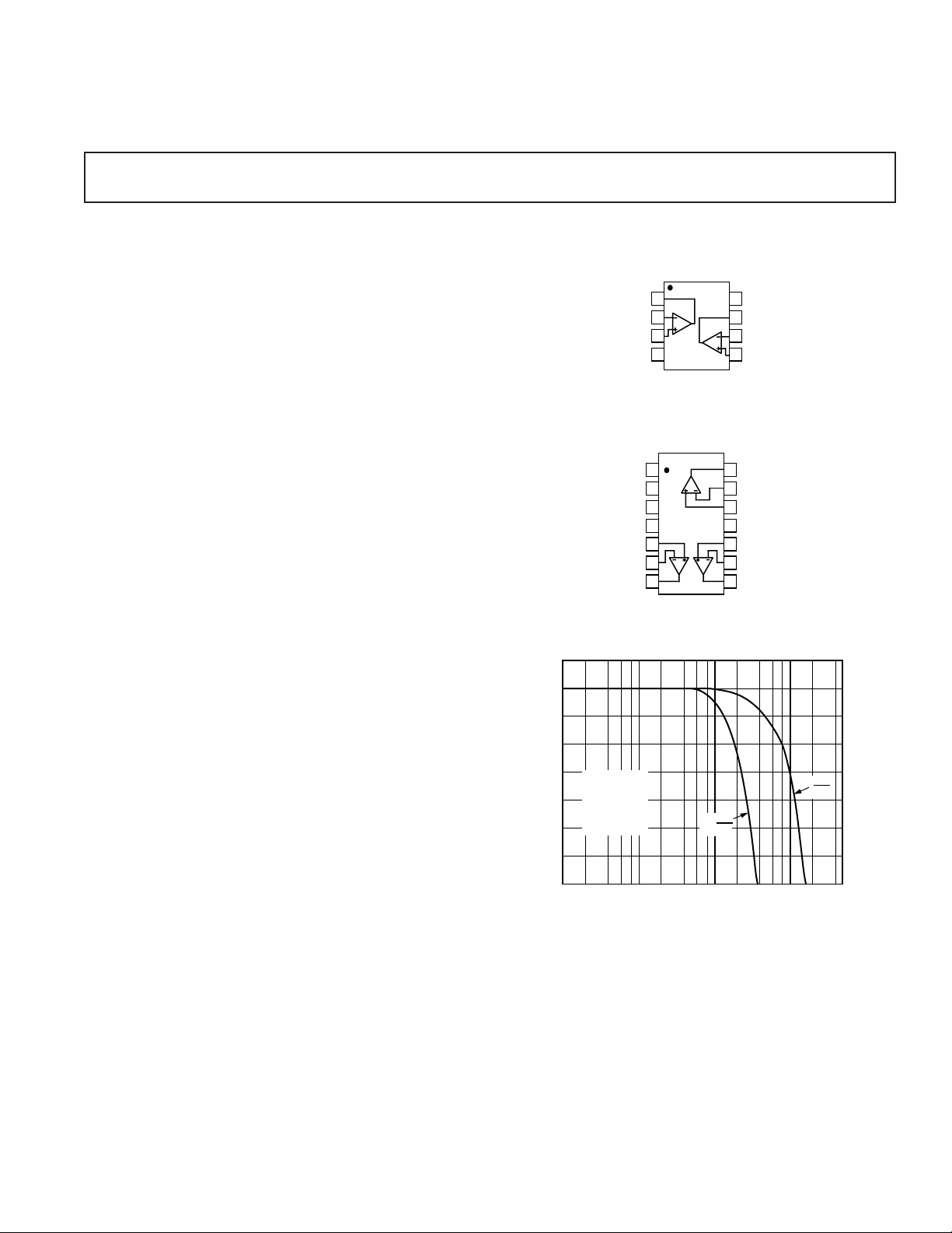
AD8073
FREQUENCY – MHz
6.1
GAIN FLATNESS – dB
6.0
5.3
0.1 500110100
5.9
5.8
5.4
5.7
5.6
5.5
6
5
4
3
2
1
0
VS = ⴞ5V
V
O
= 2V p-p
RF = RG = 1k⍀
RL = 150⍀
A
V
= ⴙ2
CLOSED-LOOP GAIN – dB
7
–1
0.1 dB
DIV
1 dB
DIV
a
FEATURES
Very Low Cost
Good Video Specifications (R
Gain Flatness of 0.1 dB to 10 MHz
0.05% Differential Gain Error
0.1ⴗ Differential Phase Error
Low Power
3.5 mA/Amplifier Supply Current
Operates on Single 5 V to 12 V Supply
High Speed
100 MHz, –3 dB Bandwidth (G = +2)
500 V/s Slew Rate
Fast Settling Time of 25 ns (0.1%)
Easy to Use
30 mA Output Current
Output Swing to 1.3 V of Rails on Single 5 V Supply
APPLICATIONS
Video Line Driver
Computer Video Plug-In Boards
RGB or S-Video Amplifier in Component Systems
= 150 ⍀)
L
Video Amplifiers
AD8072/AD8073
PIN CONFIGURATIONS
8-Lead Plastic (N), SOIC (R), and SOIC (RM) Packages
1
OUT1
2
–IN1
3
+IN1
–V
4
S
AD8072
TOP VIEW
Not to Scale
14-Lead Plastic (N), and SOIC (R) Packages
8
7
6
5
+V
S
OUT2
–IN2
+IN2
PRODUCT DESCRIPTION
The AD8072 (dual) and AD8073 (triple) are low cost, current
feedback amplifiers intended for high volume, cost sensitive
applications. In addition to being low cost, these amplifiers
deliver solid video performance into a 150 Ω load while consuming
only 3.5 mA per amplifier of supply current. Furthermore, the
AD8073 is three amplifiers in a single 14-lead narrow-body
SOIC package. This makes it ideal for applications where small
size is essential. Each amplifier’s inputs and output are accessible providing added gain setting flexibility.
These devices provide 30 mA of output current per amplifier,
and are optimized for driving one back terminated video load
(150 Ω) each. These current feedback amplifiers feature gain
flatness of 0.1 dB to 10 MHz while offering differential gain and
phase error of 0.05% and 0.1°. This makes the AD8072 and
AD8073 ideal for business and consumer video electronics.
Both will operate from a single 5 V to 12 V power supply. The
outputs of each amplifier swing to within 1.3 volts of either supply rail to accommodate video signals on a single 5 V supply.
The high bandwidth of 100 MHz, 500 V/µs of slew rate, along
with settling to 0.1% in 25 ns, make the AD8072 and AD8073
useful in many general purpose, high speed applications where a
single 5 V or dual power supplies up to ±6 V are needed. The
AD8072 is available in 8-lead plastic DIP, SOIC, and µSOIC
packages while the AD8073 is available in 14-lead plastic DIP and
SOIC packages. Both operate over the commercial temperature
range of 0°C to 70°C. Additionally, the AD8072ARM operates
over the industrial temperature range of –40°C to +85°C.
REV. D
Information furnished by Analog Devices is believed to be accurate and
reliable. However, no responsibility is assumed by Analog Devices for its
use, nor for any infringements of patents or other rights of third parties that
may result from its use. No license is granted by implication or otherwise
under any patent or patent rights of Analog Devices.
Figure 1. Large Signal Frequency Response
One Technology Way, P.O. Box 9106, Norwood, MA 02062-9106, U.S.A.
Tel: 781/329-4700 www.analog.com
Fax: 781/326-8703 © Analog Devices, Inc., 2002
Page 2

AD8072/AD8073–SPECIFICATIONS
ELECTRICAL CHARACTERISTICS
(@ TA = 25ⴗC, VS = ⴞ5 V, RL = 150 ⍀, unless otherwise noted.)
AD8072/AD8073
Parameter Conditions Min Typ Max Unit
DYNAMIC PERFORMANCE R
= 1 kΩ
F
–3 dB Bandwidth, Small Signal No Peaking, G = +2 80 100 MHz
0.1 dB Bandwidth, Small Signal No Peaking, G = +2 8 10 MHz
Slew Rate V
= 4 V Step 500 V/µs
O
Settling Time to 0.1% VO = 2 V Step 25 ns
DISTORTION/NOISE PERFORMANCE R
= 1 kΩ
F
Differential Gain f = 3.58 MHz, G = +2 0.05 0.15 %
Differential Phase f = 3.58 MHz, G = +2 0.1 0.3 Degrees
Crosstalk f = 5 MHz 60 dB
Input Voltage Noise f = 10 kHz 3 nV/√Hz
Input Current Noise f = 10 kHz (±IIN) 6 pA/√Hz
DC PERFORMANCE
Transimpedance 0.3 MΩ
Input Offset Voltage 2 6 mV
T
MIN
to T
MAX
8mV
Offset Drift 11 µV/°C
Input Bias Current (±)412µA
Input Bias Current Drift (±)12nA/°C
INPUT CHARACTERISTICS
–Input Resistance 120 Ω
+Input Resistance 1 MΩ
Input Capacitance 1.6 pF
Common-Mode Rejection Ratio V
= –3.8 V to +3.8 V 56 dB
CM
Input Common-Mode Voltage Range ±3.8 V
OUTPUT CHARACTERISTICS
+Output Voltage Swing 3 3.3 V
–Output Voltage Swing 2.25 3 V
Output Current R
= 10 Ω 30 mA
L
Short Circuit Current 80 mA
POWER SUPPLY
Operating Range ±2.5 to ± 6V
Power Supply Rejection Ratio V
= ±4 V to ±6 V 70 dB
S
Quiescent Current per Amplifier 3.5 5 mA
OPERATING TEMPERATURE RANGE 0 70 °C
Specifications subject to change without notice.
–2–
REV. D
Page 3

AD8072/AD8073
ELECTRICAL CHARACTERISTICS
(@ TA = 25ⴗC, VS = 5 V, RL = 150 ⍀ to 2.5 V, unless otherwise noted.)
AD8072/AD8073
Parameter Conditions Min Typ Max Unit
DYNAMIC PERFORMANCE R
= 1 kΩ
F
–3 dB Bandwidth, Small Signal No Peaking, G = +2 78 100 MHz
0.1 dB Bandwidth, Small Signal No Peaking, G = +2 7.8 10 MHz
Slew Rate V
= 2 V Step 350 V/µs
O
Settling Time to 0.1% VO = 2 V Step 25 ns
DISTORTION/NOISE PERFORMANCE R
Differential Gain f = 3.58 MHz, G = +2, R
Differential Phase f = 3.58 MHz, G = +2, R
= 1 kΩ
F
to 1.5 V 0.1 %
L
to 1.5 V 0.1 Degrees
L
Crosstalk f = 5 MHz 60 dB
Input Voltage Noise f = 10 kHz 3 nV/√Hz
Input Current Noise f = 10 kHz (±IIN) 6 pA/√Hz
DC PERFORMANCE
Transimpedance 0.25 MΩ
Input Offset Voltage 1.5 4 mV
T
MIN
to T
MAX
6mV
Offset Drift 9 µV/°C
Input Bias Current (±) 310µA
Input Bias Current Drift (±)10nA/°C
INPUT CHARACTERISTICS
–Input Resistance 120 Ω
+Input Resistance 1MΩ
Input Capacitance 1.6 pF
Common-Mode Rejection Ratio V
= 1.2 V to 3.8 V 54 dB
CM
Input Common-Mode Voltage Range 1.2 to 3.8 V
OUTPUT CHARACTERISTICS
Output Voltage Swing RL = 150 Ω 1.5 to 3.5 1.3 to 3.7 V
Output Voltage Swing R
Output Current R
= 1 kΩ T
L
= 10 Ω 20 mA
L
MIN
to T
MAX
1.3 to 3.7 1.1 to 3.9 V
Short Circuit Current 60 mA
POWER SUPPLY
Operating Range ±2.5 to ± 6V
Power Supply Rejection Ratio V
= 4 V to 6 V 64 dB
S
Quiescent Current per Amplifier 3 4.5 mA
OPERATING TEMPERATURE RANGE 0 70 °C
Specifications subject to change without notice.
REV. D
–3–
Page 4
AD8072/AD8073
WARNING!
ESD SENSITIVE DEVICE
ABSOLUTE MAXIMUM RATINGS
Supply Voltage . . . . . . . . . . . . . . . . . . . . . . . . . . . . . . . .13.2 V
Internal Power Dissipation
2
1
AD8072 8-Lead Plastic (N) . . . . . . . . . . . . . . . . . . 1.3 Watts
AD8072 8-Lead Small Outline (SO-8) . . . . . . . . . 0.9 Watts
AD8072 8-Lead µSOIC (RM) . . . . . . . . . . . . . . . . 0.6 Watts
AD8073 14-Lead Plastic (N) . . . . . . . . . . . . . . . . . 1.6 Watts
AD8073 14-Lead Small Outline (R) . . . . . . . . . . . 1.0 Watts
Input Voltage (Common Mode) . . . . . . . . . . . . . . . . . . . . ± V
S
Differential Input Voltage . . . . . . . . . . . . . . . . . . . . . ±1.25 V
Output Short Circuit Duration . . . . . . . . . . . . . . . . . . . . . . . .
. . . . . . . . . . . . . . . . . . . . . . Observe Power Derating Curves
Storage Temperature Range
N, R, RM Packages . . . . . . . . . . . . . . . . . . –65°C to +125°C
Lead Temperature Range (Soldering 10 sec) . . . . . . . . . 300°C
NOTES
1
Stresses above those listed under Absolute Maximum Ratings may cause perma-
nent damage to the device. This is a stress rating only; functional operation of the
device at these or any other conditions above those indicated in the operational
section of this specification is not implied. Exposure to absolute maximum rating
conditions for extended periods may affect device reliability.
2
Specification is for device in free air:
8-Lead Plastic Package: θJA = 90°C/W
8-Lead SOIC Package: θJA = 140°C/W
8-Lead µSOIC Package: θJA = 214°C/W
14-Lead Plastic Package: θJA = 75°C/W
14-Lead SOIC Package: θJA = 120°C/W
ORDERING GUIDE
Model Range Description Option
*AD8072ARM –40°C to +85°C 8-Lead µSOIC RM-8
*AD8072ARM-REEL –40°C to +85°C 13" Reel 8-Lead µSOIC RM-8
*AD8072ARM-REEL7 –40°C to +85°C 7" Reel 8-Lead µSOIC RM-8
AD8072JN 0°C to 70°C 8-Lead Plastic DIP N-8
AD8072JR 0°C to 70°C 8-Lead SOIC SO-8
AD8072JR-REEL 0°C to 70°C 13" Reel 8-Lead SOIC SO-8
AD8072JR-REEL7 0°C to 70°C 7" Reel 8-Lead SOIC SO-8
AD8073JN 0°C to 70°C 14-Lead Plastic DIP N-14
AD8073JR 0°C to 70°C 14-Lead Narrow SOIC R-14
AD8073JR-REEL 0°C to 70°C 13" Reel 14-Lead SOIC R-14
AD8073JR-REEL7 0°C to 70°C 7" Reel 14-Lead SOIC R-14
*Brand Code: HLA
Temperature Package Package
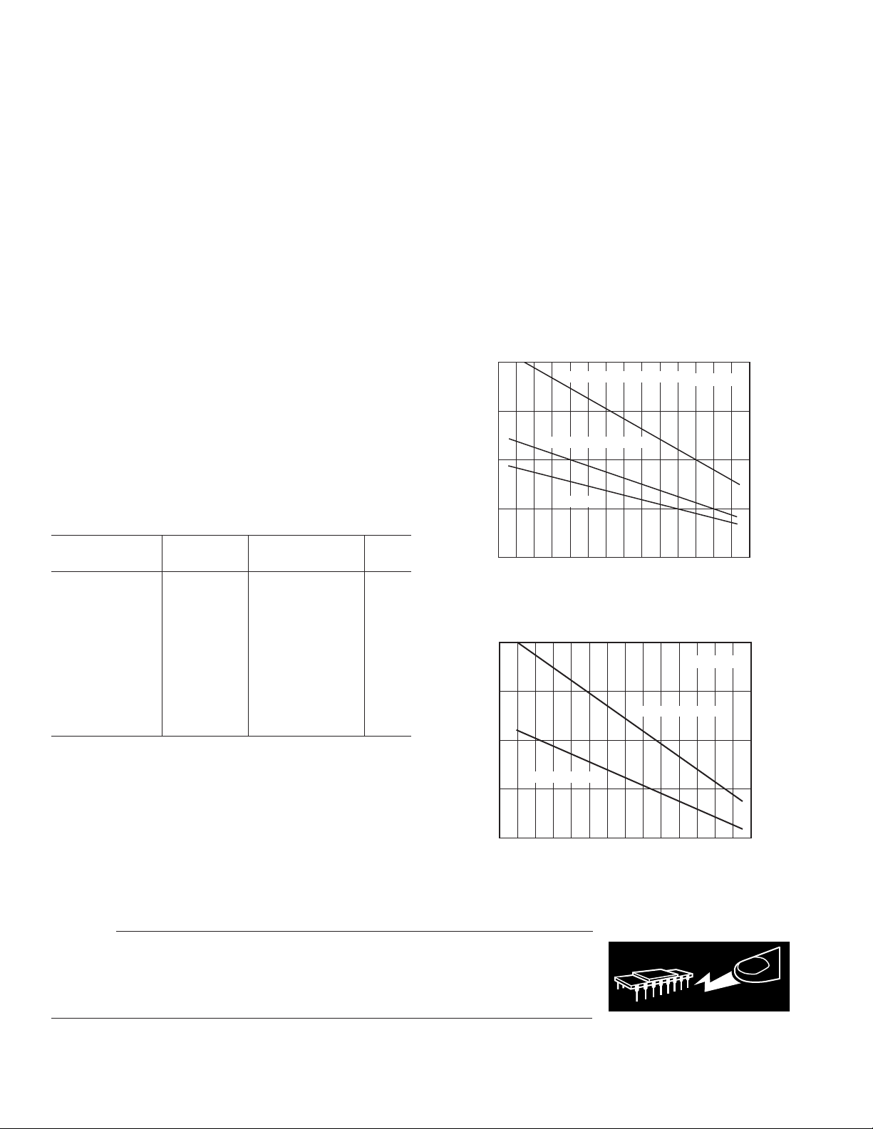
MAXIMUM POWER DISSIPATION
The maximum power that can be safely dissipated by the AD8072
and AD8073 is limited by the associated rise in junction temperature. The maximum safe junction temperature for plastic
encapsulated devices is determined by the glass transition temperature of the plastic, approximately 150°C. Exceeding this
limit temporarily may cause a shift in parametric performance
due to a change in the stresses exerted on the die by the package.
Exceeding a junction temperature of 175°C for an extended
period can result in device failure.
While the AD8072 and AD8073 are internally short circuit protected, this may not be sufficient to guarantee that the maximum
junction temperature (150°C) is not exceeded under all conditions. To ensure proper operation, it is necessary to observe the
maximum power derating curves shown in Figures 2 and 3.
2.0
8-LEAD MINI-DIP PACKAGE
1.5
8-LEAD SOIC PACKAGE
1.0
0.5
MAXIMUM POWER DISSIPATION – W
0
–50 90–40 –30 –20 –10 0 1020 30 5060708040
SOIC
AMBIENT TEMPERATURE – ⴗC
TJ = 150ⴗC
Figure 2. AD8072 Maximum Power Dissipation vs.
Temperature
2.5
TJ = 150ⴗC
2.0
14-LEAD DIP PACKAGE
1.5
14-LEAD SOIC
1.0
MAXIMUM POWER DISSIPATION – W
0.5
–30 –20 –100 1020 304050 60 80
–50 90–40
Figure 3. AD8073 Maximum Power Dissipation vs.
Temperature
CAUTION
ESD (electrostatic discharge) sensitive device. Electrostatic charges as high as 4000 V readily
accumulate on the human body and test equipment and can discharge without detection.
Although the AD8072/AD8073 feature proprietary ESD protection circuitry, permanent damage
may occur on devices subjected to high-energy electrostatic discharges. Therefore, proper ESD
precautions are recommended to avoid performance degradation or loss of functionality.
–4–
AMBIENT TEMPERATURE – ⴗC
70
REV. D
Page 5

0.00 0.03 0.07 0.08 0.08 0.08 0.09 0.08 0.08 0.07 0.06
DIFFERENTIAL GAIN – %
MIN = 0.00 MAX = 0.09 p-p/MAX = 0.09
0.12
0.10
0.08
0.06
0.04
0.02
0.00
–0.02
V
S
= 5V, RF = 1k⍀, RL = 150⍀ TO 1.5V, AV = 2
0.00 0.05 0.09 0.10 0.09 0.08 0.06 0.06 0.05 0.04 0.02
1
ST2ND3RD4TH5TH
6
TH
7TH8TH9TH10TH11
TH
MODULATING RAMP LEVEL – IRE
DIFFERENTIAL PHASE – deg
MIN = 0.00 MAX = 0.10 p-p = 0.10
0.12
0.10
0.08
0.06
0.04
0.02
0.00
–0.02
V
S
= 5V, RF = 1k⍀, RL = 150⍀ TO 1.5V, AV = 2
Typical Performance Characteristics–
AD8072/AD8073
7
6
5
4
3
VS = 5V
2
R
= 1k⍀
F
R
= 150⍀ TO 2.5V
1
CLOSED-LOOP GAIN – dB
0
0.1
0.1 10001.0 10 100
L
A
= 2
V
V
= 100mV p-p
IN
FREQUENCY – MHz
0ⴗC
70ⴗC
25ⴗC
TPC 1. Frequency Response Over Temperature; VS = 5 V
7
6
5
4
6.1
6.0
5.9
5.8
VS = ⴞ5V
= 1k⍀
R
F
= 150⍀
R
L
A
= 2
V
VIN = 100mV p-p
0.1 5001.0 10 100
GAIN FLATNESS – dB
5.7
5.6
5.5
5.4
5.3
70ⴗC
FREQUENCY – MHz
0ⴗC, 25ⴗC
TPC 4. 0.1 dB Flatness vs. Frequency Over Temperature;
V
= ±5 V
S
3
VS = ⴞ5V
2
1
CLOSED-LOOP GAIN – dB
0
0.1
0.1 10001.0 10 100
= 1k⍀
R
F
= 150⍀
R
L
A
= 2
V
V
= 100mV p-p
IN
FREQUENCY – MHz
TPC 2. Frequency Response Over Temperature; VS = ±5 V
6.1
6.0
5.9
5.8
5.7
VS = 5V
R
= 1k⍀
F
R
= 150⍀ TO 2.5V
L
5.6
A
= 2
V
GAIN FLATNESS – dB
V
= 100mV p-p
IN
5.5
REV. D
5.4
5.3
0.1 5001.0 10 100
FREQUENCY – MHz
TPC 3. 0.1 dB Flatness vs. Frequency Over Temperature;
V
= 5 V
S
70ⴗC
70ⴗC
0ⴗC, 25ⴗC
25ⴗC
0ⴗC
–5–
TPC 5. Differential Gain and Phase, VS = 5 V
0.00 0.00 0.00 –0.00 0.00 –0.01 –0.01 –0.02 –0.03 –0.03 –0.03
0.00
VS = ⴞ5V
–0.01
R
= 1k⍀
–0.02
–0.03
DIFFERENTIAL GAIN – %
–0.02
–0.04
–0.06
–0.08
–0.10
–0.12
DIFFERENTIAL PHASE – deg
F
= 150⍀
R
L
A
= 2
V
0.00 0.00 –0.00 –0.02 –0.03 –0.05 –0.07 –0.08 –0.10 –0.10 –0.10
0.02
0.00
V
= ⴞ5V
S
R
= 1k⍀
F
= 150⍀
R
L
A
= 2
V
1
ST2ND3RD4TH5TH
MIN = –0.03 MAX = 0.00 p-p/MAX = 0.03
MIN = –0.10 MAX = 0.00 p-p = 0.10
6
TH
MODULATING RAMP LEVEL – IRE
7TH8TH9TH10TH11
TPC 6. Differential Gain and Phase, VS = ±5 V
TH
Page 6

AD8072/AD8073
0
–10
SOIC PACKAGE
DRIVE AMP 2
–20
RECEIVE AMPS 1, 3 AD8073
RECEIVE AMP 1 AD8072
–30
= 5V, ⴞ5V
V
S
= 1k⍀, RL = 150⍀
R
F
–40
= 2
A
V
= 1V p-p
V
IN
–50
–60
CROSSTALK – dB
–70
–80
–90
–100
0.1 5001.0 10 100
FREQUENCY – MHz
AMP 2 OUTPUT
TPC 7. Crosstalk vs. Frequency
–40
VS = ⴞ5V
= 1k⍀
R
F
–50
= 150⍀
R
L
A
= 2
V
V
= 2V p-p
OUT
–60
–70
–80
DISTORTION – dBc
–90
–100
0.1 1
FREQUENCY – MHz
3RD
HARMONIC
HARMONIC
2ND
TPC 8. Distortion vs. Frequency; VS = ±5 V
1G
0
–20
–40
–60
–80
–100
–120
–140
–160
–180
DEGREES
100k
– ⍀
Z
T
1M
10k
100
OHMS (⍀)
DEGREES
1k
10
10k
1k
FREQUENCY – Hz
100M
10M1M100k
TPC 10. Open-Loop Transimpedance vs. Frequency
3
2
1
0
–1
–2
VS = ⴞ5V
RF = 1k⍀
–3
= 150⍀
R
L
= 200mV p-p
V
OUT
–4
–5
NORMALIZED CLOSED-LOOP GAIN – dB
10
–6
0.1 1k1 10 100
FREQUENCY – MHz
AV = 10
AV = 1
AV = 2
AV = 5
TPC 11. Normalized Frequency Response; VS = ±5 V
–40
VS = 5V
R
= 1k⍀
F
–50
R
= 150⍀ TO 2.5V
L
A
= 2
V
V
= 2V p-p
OUT
–60
–70
–80
DISTORTION – dBc
–90
–100
0.1 1 10
FREQUENCY – MHz
3RD
HARMONIC
2ND
HARMONIC
TPC 9. Distortion vs. Frequency; VS = 5 V
–6–
6.1
6.0
5.9
5.8
5.7
VS = 5V
= 2V p-p
V
O
GAIN FLATNESS – dB
5.6
5.5
5.4
5.3
= RG = 1k⍀
R
F
= 150⍀ TO 2.5V
R
L
= 2
A
V
0.1 5001 10 100
0.1 dB
DIV
FREQUENCY – MHz
TPC 12. Large Signal Frequency Response
1 dB
DIV
7
6
5
4
3
2
1
CLOSED-LOOP GAIN – dB
0
–1
REV. D
Page 7

100
VS = ⴞ5V
= 1k⍀
R
F
= 2
A
V
AD8072/AD8073
100
80
10
1
OUTPUT RESISTANCE – ⍀
0.1
0.1 5001 10 100
FREQUENCY – MHz
TPC 13. Output Resistance vs. Frequency; VS = ±5 V
50
40
30
20
10
INPUT VOLTAGE NOISE – nV/ Hz
0
1 100k10
100 1k 10k
FREQUENCY – Hz
TPC 14. Noise vs. Frequency; VS = ±5 V
60
40
20
INPUT CURRENT NOISE – pA/ Hz
0
1 100k10
100 1k 10k
FREQUENCY – Hz
TPC 15. Noise vs. Frequency; VS = ±5 V
10
VS = ⴞ5V
0
= 1k⍀
R
F
= 150⍀
R
L
AV = 2
100mV p-p ON TOP
OF V
S
0.1 5001 10 100
0.02
–PSRR
ⴙPSRR
FREQUENCY – MHz
PSRR – dB
–10
–20
–30
–40
–50
–60
–70
TPC 16. PSRR vs. Frequency
REV. D
CMRR – dB
–10
–15
–20
–25
–30
–35
–40
–45
–50
–55
–5
2V p-p
0.02
1k⍀ 1k⍀
V
IN
150⍀
V
OUT
154⍀
60.4⍀
154⍀
0.1 5001 10 100
FREQUENCY – MHz
TPC 17. CMRR vs. Frequency; VS = ±5 V
–7–
Page 8

AD8072/AD8073
1k⍀ 1k⍀
V
IN
50⍀
TPC 18. Test Circuit; Gain = +2
250mV
20ns
TPC 19. 2 V Step Response; G = +2, VS = ±5 V
V
0.1F
0.1F
R
L
150⍀
0.001F
0.001F
+
+
10F
10F
250mV
ⴙV
–V
OUT
S
S
10ns
TPC 22. 2 V Step Response; G = +2, VS = ±2.5 V
*
50mV
20ns
TPC 20. 200 mV Step Response; G = +2, VS = ±5 V
1V
20ns
TPC 21. Sine Response; G = +2, VS = ±5 V
*
VS = ±2.5 V operation is identical to VS = 5 V single supply operation.
–8–
50mV
20ns
TPC 23. 200 mV Step Response; G = +2, VS = ±2.5 V
250mV
TPC 24. Sine Response; G = +2, VS = ±2.5 V
20ns
*
REV. D
*
Page 9

AD8072/AD8073
APPLICATIONS
Overdrive Recovery
Overdrive of an amplifier occurs when the output and/or input
range are exceeded. The amplifier must recover from this overdrive
condition and resume normal operation. As shown in Figure 4,
the AD8072 and AD8073 recover within 75 ns from positive
overdrive and 30 ns from negative overdrive.
V
IN
V
OUT
1V
25ns
Figure 4. Overload Recovery; VS = ±5 V, VIN = 8 V p-p,
R
= 1 kΩ, RL = 150 Ω, G = +2
F
Bandwidth vs. Feedback Resistor Value
The closed-loop frequency response of a current feedback amplifier
is a function of the feedback resistor. A smaller feedback resistor
will produce a wider bandwidth response. However, if the feedback resistance becomes too small, the gain flatness can be
affected. As a practical consideration, the minimum value of
feedback resistance for the AD8072/AD8073 was found to be
649 Ω. For resistances below this value, the gain flatness will be
affected and more significant lot-to-lot variations in device performance will be noticed. Figure 5 shows a plot of the frequency
response of an AD8072/AD8073 at a gain of two with both feedback and gain resistors equal to 649 Ω.
6.1
6.0
5.9
5.8
5.7
VS = ⴞ5V
A
= 2
V
5.6
GAIN FLATNESS – dB
R
= 150⍀
L
V
= 0.2V p-p
O
5.5
5.4
0.1 5001 10 100
0.1 dB
DIV
RF = 2k⍀
FREQUENCY – MHz
Figure 5. Frequency Response vs. R
RF = 649⍀
1 dB
DIV
7
6
5
4
3
2
CLOSED-LOOP GAIN – dB
1
0
F
On the other hand, the bandwidth of a current feedback amplifier can be decreased by increasing the feedback resistance. This
can sometimes be useful where it is desired to reduce the noise
bandwidth of a system. As a practical matter, the maximum
value of feedback resistor was found to be 2 kΩ. Figure 5 shows
the frequency response of an AD8072/AD8073 at a gain of two
with both feedback and gain resistors equal to 2 kΩ.
Capacitive Load Drive
When an op amp output drives a capacitive load, extra phase shift
due to the pole formed by the op amp’s output impedance and
the capacitor can cause peaking or even oscillation. The top trace
of Figure 6, R
= 0 Ω, shows the output of one of the amplifiers of
S
the AD8072/AD8073 when driving a 50 pF capacitor as shown in
the schematic of Figure 7.
The amount of peaking can be significantly reduced by adding
a resistor in series with the capacitor. The lower trace of Figure 6
shows the same capacitor being driven with a 25 Ω resistor
in series with it. In general, the resistor value will have to be
experimentally determined, but 10 Ω to 50 Ω is a practical range
of values to experiment with for capacitive loads of up to a few
hundred pF.
RS = 0Ω
RS = 25Ω
50mV
20ns
Figure 6. Capacitive Low Drive
1k⍀ 1k⍀
R
S
V
= 100mV p-p R
IN
50⍀
C
L
50pF
L
1k⍀
Figure 7. Capacitive Load Drive Circuit
REV. D
–9–
Page 10

AD8072/AD8073
Crosstalk
Crosstalk between internal amplifiers may vary depending on
which amplifier is being driven and how many amplifiers are
being driven. This variation typically stems from pin location on
the package and the internal layout of the IC itself. Table I
illustrates the typical crosstalk results for a combination of
conditions.
Table I. AD8073JR Crosstalk Table (dB)
Receive Amplifier
AD8073JR
123
1 X –60 –56
Drive
Amplifier
2 –60 X –60
3 –54 –60 X
All Hostile –53 –55 –54
CONDITIONS
VS = ±5 V
= 1 kΩ, RL = 150 Ω
R
F
A
= 2
V
V
= 2 V p-p on Drive Amplifier
OUT
Layout Considerations
The specified high speed performance of the AD8072 and
AD8073 require careful attention to board layout and component selection. Proper RF
design techniques and low parasitic
component selection are mandatory.
The PCB should have a ground plane covering all unused portions
of the component side of the board to provide a low impedance
ground path. The ground plane should be removed from the
area near the input pins to reduce stray capacitance.
Chip capacitors should be used for supply bypassing. One end
of the capacitor should be connected to the ground plane and
the other within 1/8 inches of each power pin. An additional
large (4.7 µF–10 µF) tantalum electrolytic capacitor should be
connected in parallel, but not necessarily as close to the supply
pins, to provide current for fast large-signal changes at the
device’s output.
The feedback resistor should be located close to the inverting
input pin in order to keep the stray capacitance at this node to a
minimum. Capacitance variations of less than 1 pF at the inverting input will affect high speed performance.
Stripline design techniques should be used for long signal traces
(greater than approximately 1 inch). These should be designed
with a characteristic impedance of 50 Ω or 75 Ω and be properly
terminated at each end.
–10–
REV. D
Page 11

OUTLINE DIMENSIONS
Dimensions shown in inches and (mm).
AD8072/AD8073
0.210 (5.33)
MAX
0.160 (4.06)
0.115 (2.93)
0.022 (0.558)
0.014 (0.356)
0.1574 (4.00)
0.1497 (3.80)
8-Lead Plastic DIP
(N-8)
0.430 (10.92)
0.348 (8.84)
8
14
PIN 1
0.100
(2.54)
BSC
5
0.280 (7.11)
0.240 (6.10)
0.060 (1.52)
0.015 (0.38)
0.070 (1.77)
0.045 (1.15)
8-Lead Plastic SOIC
(R-8)
0.1968 (5.00)
0.1890 (4.80)
8
5
0.2440 (6.20)
41
0.2284 (5.80)
0.130
(3.30)
MIN
SEATING
PLANE
0.325 (8.25)
0.300 (7.62)
0.015 (0.381)
0.008 (0.204)
0.195 (4.95)
0.115 (2.93)
0.210 (5.33)
MAX
0.160 (4.06)
0.115 (2.93)
0.1574 (4.00)
0.1497 (3.80)
14-Lead Plastic DIP
(N-14)
0.795 (20.19)
0.725 (18.42)
14
17
PIN 1
0.022 (0.558)
0.014 (0.356)
0.100
(2.54)
BSC
8
0.070 (1.77)
0.045 (1.15)
14-Lead SOIC
(R-14)
0.3444 (8.75)
0.3367 (8.55)
14 8
71
0.280 (7.11)
0.240 (6.10)
0.060 (1.52)
0.015 (0.38)
0.130
(3.30)
MIN
SEATING
PLANE
0.2440 (6.20)
0.2284 (5.80)
0.325 (8.25)
0.300 (7.62)
0.015 (0.381)
0.008 (0.204)
0.195 (4.95)
0.115 (2.93)
PIN 1
0.0098 (0.25)
0.0040 (0.10)
SEATING
PLANE
0.0500
(1.27)
BSC
0.0688 (1.75)
0.0532 (1.35)
0.0192 (0.49)
0.0138 (0.35)
0.0098 (0.25)
0.0075 (0.19)
0.0196 (0.50)
0.0099 (0.25)
8°
0°
0.0500 (1.27)
0.0160 (0.41)
0.122 (3.10)
0.114 (2.90)
0.006 (0.15)
0.002 (0.05)
SEATING
PLANE
x 45°
0.122 (3.10)
0.114 (2.90)
85
PIN 1
0.0256 (0.65) BSC
0.120 (3.05)
0.112 (2.84)
0.018 (0.46)
0.008 (0.20)
8-Lead SOIC
(RM-8)
0.199 (5.05)
0.187 (4.75)
41
0.043 (1.09)
0.037 (0.94)
0.011 (0.28)
0.003 (0.08)
0.0098 (0.25)
0.0040 (0.10)
SEATING
PLANE
0.120 (3.05)
0.112 (2.84)
33ⴗ
27ⴗ
PIN 1
0.0500
(1.27)
BSC
0.028 (0.71)
0.016 (0.41)
0.0688 (1.75)
0.0532 (1.35)
0.0192 (0.49)
0.0138 (0.35)
0.0099 (0.25)
0.0075 (0.19)
0.0196 (0.50)
0.0099 (0.25)
8°
0°
0.0500 (1.27)
0.0160 (0.41)
x 45°
REV. D
–11–
Page 12

AD8072/AD8073
Revision History
Location Page
3/02—Data Sheet changed from REV. C to REV. D.
Edits to Package Outline . . . . . . . . . . . . . . . . . . . . . . . . . . . . . . . . . . . . . . . . . . . . . . . . . . . . . . . . . . . . . . . . . . . . . . . . . . . . . . . . . . 1
10/01—Data Sheet changed from REV. B to REV. C.
Edits to ELECTRICAL CHARACTERISTICS . . . . . . . . . . . . . . . . . . . . . . . . . . . . . . . . . . . . . . . . . . . . . . . . . . . . . . . . . . . . . . . . 3
C01066–0–3/02(D)
–12–
PRINTED IN U.S.A.
REV. D
 Loading...