

Page 1
High Gain Bandwidth Product
FEATURES
• FET input amplifier: 0.6 pA input bias current
• Stable for gains ≥8
• High speed
• 54 MHz, –3 dB bandwidth (G = +10)
• 640 V/µs slew rate
• Low noise
• 6.6 nV/√Hz
• 0.6 fA/√Hz
• Low offset voltage (1.0 mV max)
• Wide supply voltage range: 5 V to 24 V
• No phase reversal
• Low input capacitance
• Single-supply and rail-to-rail output
• Excellent distortion specs: SFDR 95 dBc @ 1 MHz
• High common-mode rejection ratio: –106 dB
• Low power: 6.5 mA typical supply current
• Low cost
• Small packaging: SOT-23-5
APPLICATIONS
• Photodiode preamplifier
• Precision high gain amplifier
• High gain, high bandwidth composite amplifier
GENERAL DESCRIPTION
The AD8067 Fast FET amp is a voltage feedback amplifier with
FET inputs offering wide bandwidth (54 MHz @ G = +10) and high
slew rate (640 V/µs). The AD8067 is fabricated in a proprietary,
dielectrically isolated eXtra Fast Complementary Bipolar process
(XFCB) that enables high speed, low power, and high performance
FET input amplifiers.
The AD8067 is designed to work in applications that require high
speed and low input bias current, such as fast photodiode
preamplifiers. As required by photodiode applications, the laser
trimmed AD8067 has excellent dc voltage offset (1.0 mV max)
and drift (15 µV/°C max).
Rev. 0
Information furnished by Analog Devices is believed to be accurate and reliable.
However, no responsibility is assumed by Analog Devices for its use, nor for any
infringements of patents or other rights of third parties that may result from its use.
Specifications subject to change without notice. No license is granted by implication
or otherwise under any patent or patent rights of Anal og Devices. Trademarks and
registered trademarks are the property of their respective companies.
Precision Fast FET
™
Op Amp
AD8067
CONNECTION DIAGRAM
SOT-23-5 (RT-5)
+V
V
1
OUT
2
–V
S
3
+IN
Figure 1. Connection Diagram (Top View)
The FET input bias current (5 pA max) and low voltage noise
(6.6 nV/√Hz) also contribute to making it appropriate for precision
applications. With a wide supply voltage range (5 V to 24 V) and
rail-to-rail output, the AD8067 is well suited to a variety of
applications that require wide dynamic range and low distortion.
The AD8067 amplifier consumes only 6.5 mA of supply current,
while capable of delivering 30 mA of load current and driving
capacitive loads of 100 pF. The AD8067 amplifier is available in a
SOT-23-5 package and is rated to operate over the industrial
temperature range, –40°C to +85°C.
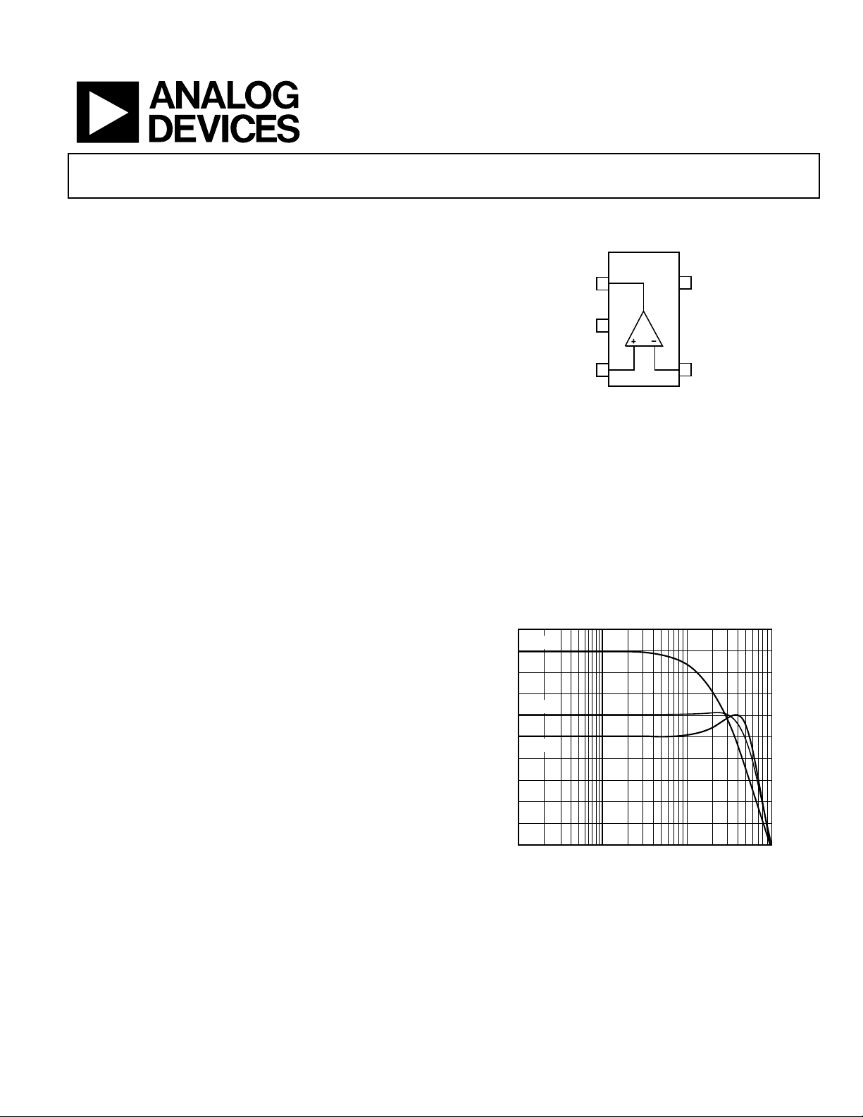
28
G = +20
26
24
22
G = +10
20
18
G = +8
GAIN – dB
16
14
12
10
8
0.1 1 10 100
Figure 2. Small Signal Frequency Respon se
One Technology Way, P.O. Box 9106, Norwood, MA 02062-9106, U.S.A.
Tel: 781.329.4700 www.analog.com
Fax: 781.326.8703 © 2002 Analog Devices, Inc. All rights reserved.
FREQUENCY – MHz
5
S
4
–IN
Page 2

AD8067
TABLE OF CONTENTS
AD8067–Specifications for ±5 V...........................................................4
Input Protection ................................................................................18
AD8067–Specifications for +5 V...........................................................5
AD8067–Specifications for ±12 V.........................................................6
Absolute Maximum Ratings ..................................................................7
Maximum Power Dissipation............................................................7
Typical Performance Characteristics .................................................... 8
Test Circuits............................................................................................13
Theory of Operation .............................................................................15
Basic Frequency Response............................................................... 15
Resistor Selection for Wideband Operation..................................16
Input and Output Overload Behavior............................................17
TABLES
Table 1. Recommended Values of RG and RF.....................................15
Table 2. RMS Noise Contributions of Photodiode Preamp............. 20
REVISION HISTORY
Revision 0: Initial Version
Capacitive Load Drive ......................................................................18
Layout, Grounding, and Bypassing Considerations.....................18
Applications............................................................................................20
Wideband Photodiode Preamp.......................................................20
Using the AD8067 at Gains of Less Than 8...................................21
Single-Supply Operation..................................................................22
High Gain, High Bandwidth Composite Amplifier......................22
Outline Dimensions ..............................................................................24
Ordering Guide .................................................................................24
Table 3. Ordering Guide........................................................................24
Rev. 0 | Page 2 of 24
Page 3

AD8067
FIGURES
Figure 1. Connection Diagram (Top View)..........................................1
Figure 32. Output Saturation Voltage vs. Temperature.................... 12
Figure 2. Small Signal Frequency Response.........................................1
Figure 3. Maximum Power Dissipation vs. Temperature for
a 4-Layer Board ...............................................................................7
Figure 4. Small Signal Frequency Response for Various Gains .........8
Figure 5. Small Signal Frequency Response for Various Supplies.....8
Figure 6. Large Signal Frequency Response for Various Supplies.....8
Figure 7. 0.1 dB Flatness Frequency Response ...................................8
Figure 8. Small Signal Frequency Response for Various C
Figure 9. Frequency Response for Various Output Amplitudes........8
Figure 10. Small Signal Frequency Response for Various RF.............9
Figure 11. Distortion vs. Frequency for Various Loads ......................9
Figure 12. Distortion vs. Frequency for Various Amplitudes.............9
Figure 13. Open-Loop Gain and Phase ................................................9
Figure 14. Distortion vs. Frequency for Various Supplies..................9
Figure 15. Distortion vs. Output Amplitude for Various Loads ........9
Figure 16. Small Signal Transient Response 5 V Supply...................10
Figure 17. Output Overdrive Recovery...............................................10
LOAD
.........8
Figure 33. Open-Loop Gain vs. Load Current for Various
Supplies.......................................................................................... 12
Figure 34. Standard Test Circuit.......................................................... 13
Figure 35. Open-Loop Gain Test Circuit........................................... 13
Figure 36. Test Circuit for Capacitive Load....................................... 13
Figure 37. CMRR Test Circuit ............................................................. 14
Figure 38. Positive PSRR Test Circuit................................................. 14
Figure 39. Output Impedance Test Circuit ........................................ 14
Figure 40. Noninverting Gain Configuration................................... 15
Figure 41. Open-Loop Frequency Response.................................... 15
Figure 42. Inverting Gain Configuration........................................... 15
Figure 43. Input and Board Capacitances.......................................... 16
Figure 44. Op Amp DC Error Sources.............................................. 17
Figure 45. Simplified Input Schematic............................................. 17
Figure 46 Current Limiting Resistor .................................................. 18
Figure 47. Guard-Ring Configurations.............................................. 18
Figure 48. Guard-Ring Layout SOT-23-5 .......................................... 18
Figure 18. Long-Term Settling Time...................................................10
Figure 19. Small Signal Transient Response ± 5 V Supply ...............10
Figure 20. Large Signal Transient Response.......................................10
Figure 21. 0.1% Short-Term Settling Time........................................10
Figure 22. Input Bias Current vs. Temperature..................................11
Figure 23. Input Offset Voltage Histogram ........................................11
Figure 24. Voltage Noise........................................................................11
Figure 25. Input Bias Current vs. Common-Mode Voltage..............11
Figure 26. Input Offset Voltage vs. Common-Mode Voltage...........11
Figure 27. CMRR vs. Frequency ..........................................................11
Figure 28. Output Impedance vs. Frequency .....................................12
Figure 29. Output Saturation Voltage vs. Output Load Current......12
Figure 30. PSRR vs. Frequency.............................................................12
Figure 31. Quiescent Current vs. Temperature for Various
Supply Voltages..............................................................................12
Figure 49. Wideband Photodiode Preamp......................................... 20
Figure 50. Photodiode Voltage Noise Contributions ....................... 20
Figure 51. Photodiode Preamplifier ................................................... 21
Figure 52. Photodiode Preamplifier Frequency Response .............. 21
Figure 53. Photodiode Preamplifier Pulse Response....................... 21
Figure 54. Gain of Less than 2 Schematic .......................................... 21
Figure 55. Gain of 2 Pulse Response .................................................. 22
Figure 56. Single-Supply Operation Schematic ................................ 22
Figure 57. AD8067/AD8009 Composite ........................................... 23
Figure 58. Gain Bandwidth Response ................................................ 23
Figure 59. Large Signal Response........................................................ 23
Figure 60. Small Signal Response........................................................ 23
Figure 61. 5-Lead Plastic Surface Mount Package ........................... 24
Rev. 0 | Page 3 of 24
Page 4
AD8067
AD8067–SPECIFICATIONS FOR ±5 V
VS = ±5 V (@ T
= +25°C, G = +10, RF = RL =1 kΩ, Unless Otherwise Noted.)
A
Parameter Conditions Min Typ Max Unit
= 0.2 V p-p
DYNAMIC
PERFORMANCE
–3 dB Bandwidth
Bandwidth for 0.1 dB Flatness
Output Overdrive Recovery Time
(Pos/Neg)
Slew Rate
Settling Time to 0.1%
V
O
= 2 V p-p
V
O
V
= 0.2 V p-p
O
= ±0.6 V
V
I
V
= 5 V Step
O
= 5 V Step
V
O
39 54 MHz
54 MHz
8 MHz
115/190 ns
500 640 V/µs
27 ns
fC = 1 MHz, 2 V p-p 95 dBc
fC = 1 MHz, 8 V p-p 84 dBc
fC = 5 MHz, 2 V p-p 82 dBc
= 1 MHz, 2 V p-p, RL = 150 Ω
f
C
72 dBc
NOISE/DISTORTION
PERFORMANCE
Spurious Free Dynamic Range (SFDR)
Input Voltage Noise f = 10 kHz 6.6 nV/√Hz
Input Current Noise f = 10 kHz 0.6 fA/√Hz
DC PERFORMANCE
Input Offset Voltage
Input Offset Voltage Drift
Input Bias Current
Input Offset Current
Open-Loop Gain
0.6 5 pA
to T
T
MIN
25 pA
MAX
0.2 1 pA
T
to T
MIN
V
O
1 pA
MAX
= ±3 V
0.2 1.0 mV
1 15 µV/°C
103 119 dB
Common-Mode Input Impedance 1000||1.5 GΩ||pF
INPUT
CHARACTERISTICS
OUTPUT
CHARACTERISTICS
Differential Input Impedance 1000||2.5 GΩ||pF
Input Common-Mode Voltage Range –5.0 2.0 V
Common-Mode Rejection Ratio (CMRR) V
Output Voltage Swing
= –1 V to +1 V –85 –106 dB
CM
RL = 1 kΩ –4.86 to +4.83
= 150 Ω
R
L
–4.92 to +4.92 V
–4.67 to +4.72 V
Output Current SFDR > 60 dBc, f = 1 MHz 30 mA
Short Circuit Current 105 mA
Capacitive Load Drive 30% over shoot 120 pF
Operating Range 5 24 V
POWER SUPPLY
Quiescent Current 6.5 6.8 mA
Power Supply Rejection Ratio (PSRR) –90 –109 dB
Rev. 0 | Page 4 of 24
Page 5

AD8067
AD8067–SPECIFICATIONS FOR +5 V
VS = +5 V (@ T
= +25°C, G = +10, RL =RF = 1 kΩ, Unless Otherwise Noted.)
A
Parameter Conditions Min Typ Max Unit
V
DYNAMIC
PERFORMANCE
–3 dB Bandwidth
Bandwidth for 0.1 dB Flatness
Output Overdrive Recovery Time (Pos/Neg)
Slew Rate
Settling Time to 0.1%
= 0.2 V p-p
O
= 2 V p-p
V
O
V
= 0.2 V p-p
O
V
= +0.6 V
I
V
= 3 V Step
O
V
= 2 V Step
O
36 54 MHz
54 MHz
8 MHz
150/200 ns
390 490 V/µs
25 ns
fC = 1 MHz, 2 V p-p 86 dBc
fC = 1 MHz, 4 V p-p 74 dBc
fC = 5 MHz, 2 V p-p 60 dBc
f
= 1 MHz, 2 V p-p, RL = 150 Ω 72 dBc
C
NOISE/DISTORTION
PERFORMANCE
Spurious Free Dynamic Range (SFDR)
Input Voltage Noise f = 10 kHz 6.6 nV/√Hz
Input Current Noise f = 10 kHz 0.6 fA/√Hz
DC PERFORMANCE
Input Offset Voltage
Input Offset Voltage Drift
Input Bias Current
Input Offset Current
Open-Loop Gain
0.5 5 pA
to T
T
MIN
25 pA
MAX
0.1 1 pA
to T
T
MIN
V
O
pA
MAX
= 0.5 V to 4.5 V
0.2 1.0 mV
1 15 µV/°C
100 117 dB
Common-Mode Input Impedance 1000||2.3 GΩ||pF
INPUT
CHARACTERISTICS
OUTPUT
CHARACTERISTICS
Differential Input Impedance 1000||2.5 GΩ||pF
Input Common-Mode Voltage Range 0 2.0 V
Common-Mode Rejection Ratio (CMRR) V
Output Voltage Swing
= 0.5 Vto 1.5 V –81 –98 dB
CM
RL = 1 kΩ 0.07 to 4.89 0.03 to 4.94
=150 Ω
R
L
0.08 to 4.83
V
V
Output Current SFDR > 60 dBc, f = 1 MHz 22 mA
Short Circuit Current 95 mA
Capacitive Load Drive 30% over shoot 120 pF
Operating Range 5 24 V
POWER SUPPLY
Quiescent Current 6.4 6.7 mA
Power Supply Rejection Ratio (PSRR) –87 –103 dB
Rev. 0 | Page 5 of 24
Page 6

AD8067
AD8067–SPECIFICATIONS FOR ±12 V
VS = ±12 V (@ T
= +25°C, G = +10, RL = RF = 1 kΩ, Unless Otherwise Noted.)
A
Parameter Conditions Min Typ Max Unit
V
DYNAMIC
PERFORMANCE
–3 dB Bandwidth
Bandwidth for 0.1 dB Flatness
Output Overdrive Recovery Time
(Pos/Neg)
Slew Rate
Settling Time to 0.1%
= 0.2 V p-p
O
= 2 V p-p
V
O
V
= 0.2 V p-p
O
= ±1.5 V 75/180 ns
V
I
V
= 5 V Step
O
= 5 V Step
V
O
39 54 MHz
53 MHz
8 MHz
500 640 V/µs
27 ns
fC = 1 MHz, 2 V p-p 92 dBc
fC = 1 MHz, 20 V p-p 84 dBc
fC = 5 MHz, 2 V p-p 74 dBc
fC = 1 MHz, 2V p-p, RL = 150 Ω 72 dBc
NOISE/DISTORTION
PERFORMANCE
Spurious Free Dynamic Range (SFDR)
Input Voltage Noise f = 10 kHz 6.6 nV/√Hz
Input Current Noise f = 10 kHz 0.6 fA/√Hz
DC PERFORMANCE
Input Offset Voltage
Input Offset Voltage Drift
Input Bias Current
Input Offset Current
Open-Loop Gain
1.0 5 pA
to T
T
MIN
25 pA
MAX
0.2 1 pA
to T
T
MIN
V
O
pA
MAX
= ±10 V
0.2 1.0 mV
1 15 µV/°C
107 119 dB
Common-Mode Input Impedance 1000||1.5 GΩ||pF
INPUT
CHARACTERISTICS
OUTPUT
CHARACTERISTICS
Differential Input Impedance 1000||2.5 GΩ||pF
Input Common-Mode Voltage Range –12.0 9.0 V
Common-Mode Rejection Ratio (CMRR) V
Output Voltage Swing
= –1 V to +1 V –89 –108 dB
CM
RL = 1 kΩ –11.70 to +11.70
= 500 Ω
R
L
–11.85 to +11.84 V
–11.31 to +11.73 V
Output Current SFDR > 60 dBc, f = 1 MHz 26 mA
Short Circuit Current 125 mA
Capacitive Load Drive 30% over shoot 120 pF
Operating Range 5 24 V
POWER SUPPLY
Quiescent Current 6.6 7.0 mA
Power Supply Rejection Ratio (PSRR) –86 –97 dB
Rev. 0 | Page 6 of 24
Page 7
AD8067
ABSOLUTE MAXIMUM RATINGS
Parameter Rating
Supply Voltage 26.4 V
Power Dissipation See Figure 3
Common-Mode Input Voltage VEE – 0.5 V to VCC + 0.5 V
Differential Input Voltage 1.8 V
Storage Temperature –65°C to +125°C
Operating Temperature Range –40°C to +85°C
Lead Temperature Range
300°C
(Soldering 10 sec)
Junction Temperature 150°C
Stresses above those listed under Absolute Maximum Ratings may cause
permanent damage to the device. This is a stress rating only and functional
operation of the device at these or any other conditions above those
indicated in the operational section of this specification is not implied.
Exposure to absolute maximum rating conditions for extended periods may
affect device reliability.
Maximum Power Dissipation
The associated raise in junction temperature (TJ) on the die limits
the maximum safe power dissipation in the AD8067 package. At
approximately 150°C, which is the glass transition temperature, the
plastic will change its properties. Even temporarily exceeding this
temperature limit may change the stresses that the package exerts
on the die, permanently shifting the parametric performance of the
AD8067. Exceeding a junction temperature of 175°C for an
extended period of time can result in changes in the silicon devices,
potentially causing failure.
If the RMS signal levels are indeterminate, then consider the worst
V
case, when
In single-supply operation with RL referenced to V
V
= VS/2.
OUT
Airflow will increase heat dissipation effectively, reducing θ
= VS/4 for RL to midsupply:
OUT
()
IVP
SSD
2
()
/V
4
S
+×=
R
L
, worst case is
S–
. In
JA
addition, more metal directly in contact with the package leads
from metal traces, through holes, ground, and power planes will
reduce the θ
.
JA
Figure 3 shows the maximum safe power dissipation in the package versus ambient temperature for the SOT-23-5 (180°C/W)
package on a JEDEC standard 4-layer board. θ
values are
JA
approximations.
It should be noted that for every 10°C rise in temperature, I
B
approximately doubles (See Figure 22).
2.0
1.5
The power dissipated in the package (P
) is the sum of the
D
quiescent power dissipation and the power dissipated in the
package due to the load drive. The quiescent power is the voltage
between the supply pins (V
) times the quiescent current (IS).
S
Assuming the load (RL) is referenced to midsupply, the total drive
power is V
and some in the load (V
/2 × I
S
, some of which is dissipated in the package
OUT
× I
OUT
). The difference between the
OUT
total drive power and the load power is the drive power dissipated
in the package. RMS output voltages should be considered.
D
If RL is referenced to V
total drive power is
V
()
+=
()
S
IVP
SSD
2
as in single-supply operation, then the
S–
× I
.
OUT
VV
×+×=
V
OUTS
R
OUT
–
L
PowerLoad–PowerDriveTotalPowerQuiescentP
2
R
L
1.0
SOT-23-5
0.5
MAXIMUM POWER DISSAPATION– W
0
–30 –20 –10 8010 20 30 40 50 60 70
–40
Figure 3. Maximum Power Dissipation vs. Temperature for a 4-Layer Board
0
AMBIENT TEMPERATURE – °C
Rev. 0 | Page 7 of 24
Page 8
AD8067
TYPICAL PERFORMANCE CHARACTERISTICS
Default Conditions VS = ±5 V (@ TA = +25°C, G = +10, RL = RF = 1 kΩ, Unless Otherwise Noted.)
28
G = +20
26
24
22
G = +10
20
G = +8
18
G = +6
GAIN – dB
16
14
12
10
8
1 10 100
FREQUENCY – MHz
V
= 200mV p-p
OUT
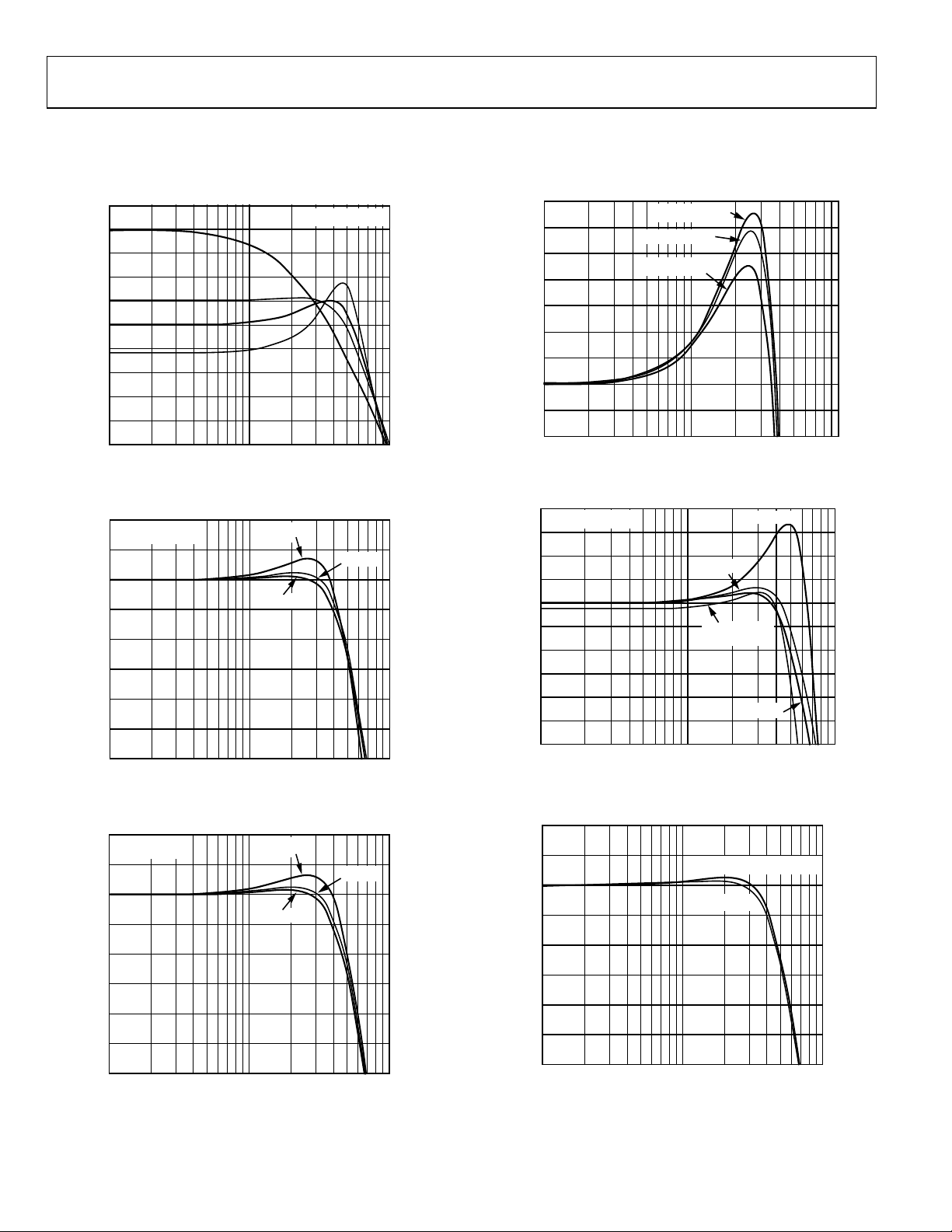
Figure 4. Small Signal Frequency Response for Various Gains
22
V
= 200mV p-p
OUT
21
20
19
18
GAIN – dB
17
16
15
14
1 10 100
FREQUENCY – MHz
V
= +5V
S
VS = ±12V
V
= ±5V
S
Figure 5. Small Signal Frequency Response for Various Supplies
22
V
= 2V p-p
OUT
21
20
19
18
GAIN – dB
17
16
15
14
1 10 100
FREQUENCY – MHz
V
= +5V
S
VS = ±12V
V
= ±5V
S
Figure 6. Large Signal Frequency Response for Various Supplies
20.7
20.6
20.5
20.4
20.3
20.2
GAIN – dB
20.1
20.0
19.9
19.8
1 10 100
V
OUT
V
= 0.7V p-p
OUT
= 1.4V p-p
V
OUT
FREQUENCY – MHz
Figure 7. 0.1 dB Flatness Frequency Response
24
V
= 200mV p-p
OUT
23
22
21
20
19
GAIN – dB
18
17
16
15
14
1 10 100
FREQUENCY – MHz
Figure 8. Small Signal Frequency Response for Various C
22
21
20
19
18
GAIN – dB
17
16
15
14
1 10 100
FREQUENCY – MHz
Figure 9. Frequency Response for Various Output Amplitudes
= 0.2V p-p
CL = 25pF
CL = 100pF
R
SNUB
V
V
= 4V p-p
OUT
CL = 100pF
= 24.9Ω
CL = 5pF
= 0.2V p-p, 2V p-p
OUT
LOAD
Rev. 0 | Page 8 of 24
Page 9

AD8067
22
V
= 200mV p-p
OUT
21
20
19
18
GAIN – dB
17
16
15
14
1 10 100
FREQUENCY – MHz
RF = 2kΩ
= 499Ω
R
F
RF = 1kΩ
Figure 10. Small Signal Frequency Response for Various R
F
90
80
70
60
50
40
GAIN – dB
30
20
10
0
–10
0.01 0.1 1 10 100 1k
FREQUENCY – MHz
PHASE
GAIN
Figure 13. Open-Loop Gain and Phase
120
90
60
30
0
–30
–60
–90
–120
–150
–180
PHASE – Degrees
–40
–50
–60
–70
–80
–90
–100
DISTORTION – dBc
–110
–120
–130
–140
0.1 1 10 100
R
LOAD
HD2
HD2 R
= 1kΩ
HD3 R
= 150Ω
LOAD
= 1kΩ
LOAD
FREQUENCY – MHz
HD3 R
V
OUT
LOAD
= 2V p-p
G = +10
V
Figure 11. Distortion vs. Frequency for Various Loads
–20
VS = ±12V
G = +10
–40
–60
–80
HD2 V
= 20V p-p
OUT
HD3 V
= 2V p-p
–100
DISTORTION – dBc
–120
–140
0.1 1 10 100
FREQUENCY – MHz
HD3 V
HD2 V
= 20V p-p
OUT
OUT
OUT
= 2V p-p
Figure 12. Distortion vs. Frequency for Various Amplitudes
= ±5V
S
= 150Ω
–40
G = +10
= 2V p-p
V
OUT
–50
–60
–70
–80
–90
HD2 VS =±5V
–100
DISTORTION – dBc
–110
–120
–130
–140
0.1 1 10 100
HD2 V
=±12V
S
HD3 VS =±5V
FREQUENCY – MHz
HD3 VS =±12V
Figure 14. Distortion vs. Frequency for Various Supplies
–30
VS =±12V
f = 1MHz
–40
G = +10
–50
–60
–70
–80
–90
DISTORTION – dBc
–100
–110
–120
–130
HD2 R
0 2 4 6 8 10 12 14 16 18 20 22 24
= 150
LOAD
HD2 R
Ω
HD3 R
= 1k
Ω
LOAD
HD3 R
OUTPUT AMPLITUDE – V p-p
LOAD
LOAD
= 150
= 1k
Ω
Ω
Figure 15. Distortion vs. Output Amplitude for Various Loads
Rev. 0 | Page 9 of 24
Page 10

AD8067
G = +10
V
= 20mV p-p
IN
50mV/DIV 25ns/DIV
Figure 16. Small Signal Transient Response 5 V Supply
10V
IN
V
OUT
G = +10
1.5V
CL = 100pF
C
= 0pF
L
50mV/DIV 25ns/DIV
G = +10
= 20mV p-p
V
IN
Figure 19. Small Signal Transient Response ± 5 V Supply
VS = ±12V
= 2V p-p
V
IN
G = +10
2V/DIV
200ns/DIV
Figure 17. Output Overdrive Recovery
VIN(100mV/DIV)
V
– 10VIN (5mV/DIV)
OUT
Figure 18. Long-Term Settling Time
5µs/DIV
+0.1%
–0.1%
5V/DIV
50ns/DIV
Figure 20. Large Signal Transient Response
V
(1V/DIV) G = +10
OUT
V
– 10VIN (5mV/DIV)
OUT
VIN(100mV/DIV)
t
= 0
5ns/DIV
+0.1%
–0.1%
Figure 21. 0.1% Short-Term Settling Time
Rev. 0 | Page 10 of 24
Page 11

AD8067
14
12
10
8
6
VS = ±12V
4
INPUT BIAS CURRENT – pA
2
= ±5V
V
0
25 35 45 55 65 75 85
TEMPERATURE – °C
S
Figure 22. Input Bias Current vs. Temperature
10
8
6
4
2
0
–2
–4
INPUT BIAS CURRENT – pA
–6
–8
–10
–14–12–10–8–6–4–202468101214
VS = ±5V VS = +5VVS = ±12V
COMMON-MODE VOLTAGE – V
Figure 25. Input Bias Current vs. Common-Mode Voltage
1800
1600
1400
1200
1000
800
COUNT
600
400
200
0
–1 0 1
INPUT OFFSET VOLTAGE – mV
N = 12255
SD = 0.203
MEAN = –0.033
Figure 23. Input Offset Voltage Histogram
1000
100
NOISE – nV/ Hz
10
5
4
3
2
1
0
–1
–2
INPUT OFFSET VOLTAGE – mV
–6
–4
–5
–14 –12 –10 –8 –6 –4 –2 0 2 4 6 8 10 12 14
VS = ±5V
COMMON-MODE VOLTAGE – V
V
S
V
= ±12V
= +5V
S
Figure 26. Input Offset Voltage vs. Common-Mode Voltage
–40
–50
–60
–70
–80
CMRR – dB
–90
–100
1
1 10 100 1k 10k 100k 1M 10M 100M
FREQUENCY – Hz
Figure 24. Voltage Noise
Rev. 0 | Page 11 of 24
–110
–120
0.1 101 100
FREQUENCY – MHz
Figure 27. CMRR vs. Fre quency
Page 12

AD8067
100
G = +10
10
Ω
1
0.1
OUTPUT IMPEDANCE –
0.01
0.001
0.01 10 1000.1 1 1000
Figure 28. Output Impedance vs. Frequency
0.30
0.25
0.20
0.15
0.10
0.05
OUTPUT SATURATION VOLTAGE – V
0
0 5 10 15 20 25 30 35 40
Figure 29. Output Saturation Voltage vs. Output Load Current
FREQUENCY – MHz
VCC– V
I
– mA
LOAD
OH
VOL– V
6.7
6.6
6.5
6.4
6.3
6.2
QUIESCENT CURRENT – mA
6.1
6.0
–40–200 20406080
EE
Figure 31. Quiescent Current vs. Temperature for Various Supply Voltages
200
RL = 1k
180
160
140
120
100
80
60
40
OUTPUT SATURATION VOLTAGE – mV
20
0
–40–200 20406080
Ω
TEMPERATURE – °C
(VCC– VOH), (VOL– VEE), VS =±12V
– VOH), (VOL– VEE), VS =±5V
(V
CC
V
CC
V
OL
TEMPERATURE –°C
VS = ±12V
VS = ±5V
VS = +5V
– VOH, VS = +5V
– VEE, VS = +5V
Figure 32. Output Saturation Voltage vs. Temperature
0
–10
–20
–30
–10
–50
PSRR – dB
–60
–70
–80
–90
–100
0.01 0.1 1 10 100
FREQUENCY – MHz
–PSRR
+PSRR
Figure 30. PSRR v s. Frequency
Rev. 0 | Page 12 of 24
140
130
120
110
100
90
80
OPEN-LOOP GAIN – dB
70
60
50
0 5 10 15 20 25 30 35 40
V
=±5V
S
V
I
LOAD
= +5V
S
VS =±12V
– mA
Figure 33. Open-Loop Gain vs. Load Current for Various Supplies
Page 13

AD8067
TEST CIRCUITS
+V
CC
10µF
+
0.1µF
49.9Ω
A
V
1kΩ
= 10
4
AD8067
3
5
RL = 1kΩ
V
OUT
1
2
0.1µF
10µF
+
–V
EE
110Ω
V
IN
Figure 34. Standard Test Circuit
+V
CC
10µF
+
0.1µF
V–
110Ω
100Ω
1kΩ
4
AD8067
3
5
1
2
0.1µF
1kΩ
V
OUT
V
OUT
=
A
OL
V–
10µF
+
–V
EE
Figure 35. Open-Loop Gain Test Circuit
+V
CC
10µF
+
0.1µF
49.9Ω
1kΩ
4
AD8067
3
5
2
0.1µF
R
C
SNUB
LOAD
1kΩ
V
OUT
1
110Ω
V
IN
10µF
= 10
A
V
–V
+
EE
Figure 36. Test Circuit for Capacitive Load
Rev. 0 | Page 13 of 24
Page 14

AD8067
V
T
110Ω
1kΩ
+V
CC
10µF
+
0.1µF
IN
110Ω
1kΩ
4
AD8067
3
5
1
2
0.1µF
10µF
+
–V
EE
1kΩ
V
OUT
Figure 37. CMRR Test Circuit
V
IN
110Ω
100Ω
1kΩ
4
AD8067
3
+V
CC
5
V
1
2
0.1µF
OU
1kΩ
10µF
+
–V
EE
Figure 38. Positive PSRR Test Circuit
+V
CC
10µF
+
0.1µF
110Ω
100Ω
1kΩ
5
4
AD8067
3
–V
1
2
EE
NETWORK ANALYZER
0.1µF
10µF
+
Figure 39. Output Impedance Test Circuit
V
OUT
Rev. 0 | Page 14 of 24
Page 15

AD8067
T
THEORY OF OPERATION
The AD8067 is a low noise, wideband, voltage feedback operational
amplifier that combines a precision JFET input stage with Analog
Devices’ dielectrically isolated eXtra Fast Complementary Bipolar
(XFCB) process BJTs. Operating supply voltages range from 5 V
to 24 V. The amplifier features a patented rail-to-rail output stage
capable of driving within 0.25 V of either power supply while
sourcing or sinking 30 mA. The JFET input, composed of
N-channel devices, has a common-mode input range that includes
the negative supply rail and extends to 3 V below the positive
supply. In addition, the potential for phase reversal behavior has
been eliminated for all input voltages within the power supplies.
The combination of low noise, dc precision, and high bandwidth
makes the AD8067 uniquely suited for wideband, very high input
impedance, high gain buffer applications. It will also prove useful
in wideband transimpedance applications, such as a photodiode
interface, that require very low input currents and dc precision.
90
80
70
60
50
40
GAIN – dB
30
20
10
0
–10
0.01 0.1 1 10 100 1k
GAIN
FREQUENCY – MHz
PHASE
Figure 41. Open-Loop Frequency Response
120
90
60
30
0
–30
–60
–90
–120
–150
–180
PHASE – Degrees
Basic Frequency Response
The AD8067’s typical open-loop response (see Figure 41) shows a
phase margin of 60° at a gain of +10. Typical configurations for
noninverting and inverting voltage gain applications are shown in
Figure 40 and Figure 42.
The closed-loop frequency response of a basic noninverting gain
configuration can be approximated using the equation:
R
()
GBPFrequencydB–LoopClosed
1+=GF/RRGainDC
GBP is the gain bandwidth product of the amplifier. Typical GBP
for the AD8067 is 300 MHz. See Table 1 for recommended values
of R
and RF.
G
GainNoiseionConfiguratngNoninverti
+
V
S
R
V
I
SIGNAL
SOURCE
R
X
S
+
AD8067
–
R
G
0.1µF
–V
S
R
F
FOR BEST PERFORMANCE,
+ RX = RG || R
SET R
S
Figure 40. Noninverting Gain Configuration
+
10µF
10µF0.1µF
+
G
×=3
()
R
LOAD
F
RR
+
GF
R
F
1
+=
R
G
+
V
OU
–
The bandwidth formula only holds true when the phase margin of
the application approaches 90°, which it will in high gain configurations. The bandwidth of the AD8067 used in a G = +10 buffer
is 54 MHz, considerably faster than the 30 MHz predicted by the
closed loop –3 dB frequency equation. This extended bandwidth is
due to the phase margin being at 60° instead of 90°. Gains lower
than +10 will show an increased amount of peaking, as shown in
Figure 4. For gains lower than +7, use the AD8065, a unity gain
stable JFET input op amp with a unity gain bandwidth of 145 MHz,
or refer to the Applications section for using the AD8067 in a gain
of 2 configuration.
Gain RG (Ω) RF (kΩ) BW (MHz)
10 110 1 54
20 49.9 1 15
50 20 1 6
100 10 1 3
Table 1. Recommended Values of RG and R
+
V
S
R
X
+
F
+
10µF0.1µF
AD8067
R
–
R
V
I
SIGNAL
SOURCE
R
S
G
FOR BEST PERFORMANCE, SET RX = (RS + RG) || R
–V
S
R
F
LOAD
+
V
10µF0.1µF
+
OUT
–
F
Figure 42. Inverting Gain Configuration
Rev. 0 | Page 15 of 24
Page 16

AD8067
T
For inverting voltage gain applications, the source impedance of the
input signal must be considered because that will set the application’s noise gain as well as the apparent closed-loop gain. The basic
frequency equation for inverting applications is below.
+
RR
Ω.
SG
++
RRR
SGF
++
RRR
SGF
+
RR
SG
×=3
(GBP) FrequencydB – Loop Closed
R
F
–GainDC
=
+
RR
SG
GBP is the gain bandwidth product of the amplifier, and RS is the
signal source resistance.
=
GainNoiseionConfiguratInverting
It is important that the noise gain for inverting applications be kept
above 6 for stability reasons. If the signal source driving the inverter
is another amplifier, take care that the driving amplifier shows low
output impedance through the frequency span of the expected
closed-loop bandwidth of the AD8067.
Resistor Selection for Wideband Operation
Voltage feedback amplifiers can use a wide range of resistor values
to set their gain. Proper design of the application’s feedback
network requires consideration of the following issues:
• Poles formed by the amplifier’s input capacitances with the
resistances seen at the amplifier’s input terminals
• Effects of mismatched source impedances
• Resistor value impact on the application’s output
voltage noise
• Amplifier loading effects
The AD8067 has common-mode input capacitances (CM) of 1.5 pF
and a differential input capacitance (C
in Figure 43. The source impedance driving the positive input of a
noninverting buffer will form a pole primarily with the amplifier’s
common-mode input capacitance as well as any parasitic
capacitance due to the board layout (C
obtainable bandwidth. For G = +10 buffers, this bandwidth limit
will become apparent for source impedances >1 k
) of 2.5 pF. This is illustrated
D
). This will limit the
PAR
R
S
+
V
I
–
SIGNAL SOURCE
C
PAR
C
PAR
Figure 43. Input and Board Capacitances
+
C
C
D
–
R
G
M
C
M
R
F
V
There will be a pole in the feedback loop response formed by the
source impedance seen by the amplifier’s negative input (R
RF)
G
and the sum of the amplifier’s differential input capacitance,
common-mode input capacitance, and any board parasitic
capacitance. This will decrease the loop phase margin and can
cause stability problems, i.e., unacceptable peaking and ringing
in the response. To avoid this problem it is recommended that the
resistance at the AD8067’s negative input be kept below 200
Ω for
all wideband voltage gain applications.
Matching the impedances at the inputs of the AD8067 is also
recommended for wideband voltage gain applications. This will
minimize nonlinear common-mode capacitive effects that can
significantly degrade settling time and distortion performance.
The AD8067 has a low input voltage noise of 6.6 nV/√Hz. Source
resistances greater than 500
Ω at either input terminal will notably
increase the apparent Referred to Input (RTI) voltage noise of the
application.
The amplifier must supply output current to its feedback network,
as well as to the identified load. For instance, the load resistance
presented to the amplifier in Figure 40 is R
R
of 100 Ω, RF of 1 kΩ, and RG of 100 Ω, the amplifier will be
LOAD
driving a total load resistance of about 92
an issue as R
decreases. The AD8067 is rated to provide 30 mA of
F
(RF + RG). For an
LOAD
Ω. This becomes more of
low distortion output current. Heavy output drive requirements
also increase the part’s power dissipation and should be taken
into account.
+
OU
–
Rev. 0 | Page 16 of 24
Page 17

AD8067
S
DC ERROR CALCULATIONS
Figure 44 illustrates the primary dc errors associated with a voltage
feedback amplifier. For both inverting and noninverting
configurations:
VVtodueErrorVoltageOutput
=
OSOS
+
RI ItodueErrorVoltageOutput ×
×=
SBB
+
R
Total error is the sum of the two.
DC common-mode and power supply effects can be added by
modeling the total V
with the expression:
OS
(nom)V(tot)V
OSOS
∆V
PSR
∆V
CMS
++=
CMR
VOS (nom) is the offset voltage specified at nominal conditions
(1 mV max). ∆VS is the change in power supply voltage from
nominal conditions.
minimum). ∆
nominal test conditions.
PSR is power supply rejection (90 dB
V
is the change in common-mode voltage from
CM
CMR is common-mode rejection (85 dB
minimum for the AD8067).
R
F
RR
+
FG
R
G
RR
GF
RI–
G
F–B
Input and Output Overload Behavior
A simplified schematic of the AD8067 input stage is shown in
Figure 45. This shows the cascoded N-channel JFET input pair,
the ESD and other protection diodes, and the auxiliary NPN
input stage that eliminates phase inversion behavior.
When the common-mode input voltage to the amplifier is driven
to within approximately 3 V of the positive power supply, the input
JFET’s bias current will turn off, and the bias of the NPN pair will
turn on, taking over control of the amplifier. The NPN differential
pair now sets the amplifier’s offset, and the input bias current is
now in the range of several tens of microamps. This behavior is
illustrated in Figure 25 and Figure 26. Normal operation resumes
when the common-mode voltage goes below the 3 V from the
positive supply threshold.
The output transistors have circuitry included to limit the extent
of their saturation when the output is overdriven. This improves
output recovery time. A plot of the output recovery time for the
AD8067 used as a G = +10 buffer is shown in Figure 17.
V
V
THRESHOLD
CONTROL
SWITCH
CC
V
CC
TO REST OF AMP
V
CC
R
G
V
–
+
I
+VOS–
–
–
I
B
R
S
+
IB+
V
+
–
OUT
V
N
V
EE
V
P
V
EE
V
BIA
Figure 44. Op Amp DC Error Sources
V
EE
Figure 45. Simplified Input Schematic
Rev. 0 | Page 17 of 24
Page 18

AD8067
+
Input Protection Layout, Grounding, and Bypassing
The inputs of the AD8067 are protected with back-to-back diodes
between the input terminals as well as ESD diodes to either power
supply. The result is an input stage with picoamp level input
currents that can withstand 2 kV ESD events (human body model)
with no degradation.
Excessive power dissipation through the protection devices will
destroy or degrade the performance of the amplifier. Differential
voltages greater than 0.7 V will result in an input current of
approximately (|
V
– V– | – 0.7 V)/(RI + RG)), where RI and RG are
+
the resistors (see Figure 46). For input voltages beyond the positive
supply, the input current will be about (
V
– VCC – 0.7 V)/RI. For
I
input voltages beyond the negative supply, the input current will be
about (
V
– VEE + 0.7 V)/RI. For any of these conditions, RI should
I
be sized to limit the resulting input current to 50 mA or less.
R
–
RI > ( |V+ – V– | –0.7V)/50mA
FOR LARGE |V
V
I
– V– |
I
+
AD8067
R
F
R
G
RI > (VI– VEE + 0.7V)/50mA
R
> (VI– VCC– 0.7V)/50mA
I
FOR V
BEYOND
I
+
SUPPLY VOLTAGES
V
OUT
–
Figure 46. Current Limiting Resistor
Capacitive Load Drive
Capacitive load introduces a pole in the amplifier loop response
due to the finite output impedance of the amplifier. This can cause
excessive peaking and ringing in the response. The AD8067 with a
gain of +10 will handle up to a 30 pF capacitive load without an
excessive amount of peaking (see Figure 8). If greater capacitive
load drive is required, consider inserting a small resistor in series
with the load (24.9
drive capability also increases as the gain of the amplifier increases.
Ω is a good value to start with). Capacitive load
Considerations
LAYOUT
In extremely low input bias current amplifier applications, stray
leakage current paths must be kept to a minimum. Any voltage
differential between the amplifier inputs and nearby traces will set
up a leakage path through the PCB. Consider a 1 V signal and
100G
Ω to ground present at the input of the amplifier. The resultant
leakage current is 10 pA; this is ten times the input bias current of
the amplifier. Poor PCB layout, contamination, and the board
material can create large leakage currents. Common contaminants
on boards are skin oils, moisture, solder flux, and cleaning agents.
Therefore, it is imperative that the board be thoroughly cleaned and
the board surface be free of contaminants to fully take advantage of
the AD8067’s low input bias currents.
To significantly reduce leakage paths, a guard ring/shield around
the inputs should be used. The guard ring circles the input pins and
is driven to the same potential as the input signal, thereby reducing
the potential difference between pins. For the guard ring to be completely effective, it must be driven by a relatively low impedance
source and should completely surround the input leads on all sides,
above, and below, using a multilayer board (see Figure 47). The
SOT-23-5 package presents a challenge in keeping the leakage paths
to a minimum. The pin spacing is very tight, so extra care must be
used when constructing the guard ring (see Figure 48 for
recommended guard-ring construction).
GUARD RING
GUARD RING
INVERTING
Figure 47. Guard-Ring Configurations
NON-INVERTING
V
OUT
–V
+IN
AD8067
INVERTING
+V
–IN
V
OUT
AD8067
–V
+IN
NONINVERTING
+V
–IN
Figure 48. Guard-Ring Layout SOT-23-5
Rev. 0 | Page 18 of 24
Page 19

AD8067
GROUNDING
To minimize parasitic inductances and ground loops in high speed,
densely populated boards, a ground plane layer is critical.
Understanding where the current flows in a circuit is critical in the
implementation of high speed circuit design. The length of the
current path is directly proportional to the magnitude of the
parasitic inductances and thus the high frequency impedance of the
path. Fast current changes in an inductive ground return will create
unwanted noise and ringing.
POWER SUPPLY BYPASSING
Power supply pins are actually inputs and care must be taken to
provide a clean, low noise dc voltage source to these inputs. The
bypass capacitors have two functions:
1. Provide a low impedance path for unwanted frequencies
from the supply inputs to ground, thereby reducing the
effect of noise on the supply lines
The length of the high frequency bypass capacitor leads is critical.
A parasitic inductance in the bypass grounding will work against
the low impedance created by the bypass capacitor. Because load
currents flow from supplies as well as ground, the load should be
placed at the same physical location as the bypass capacitor ground.
For large values of capacitors, which are intended to be effective at
lower frequencies, the current return path length is less critical.
2. Provide localized charge storage—this is usually
accomplished with larger electrolytic capacitors
Decoupling methods are designed to minimize the bypassing
impedance at all frequencies. This can be accomplished with a
combination of capacitors in parallel to ground. Good quality
ceramic chip capacitors (X7R or NPO) should be used and always
kept as close to the amplifier package as possible. A parallel
combination of a 0.1 µF ceramic and a 10 µF electrolytic, covers a
wide range of rejection for unwanted noise. The 10 µF capacitor is
less critical for high frequency bypassing, and in most cases, one
per supply line is sufficient.
Rev. 0 | Page 19 of 24
Page 20

AD8067
(
(
APPLICATIONS
bandwidth in half will result in a flat frequency response, with
about 5% transient overshoot.
Wideband Photodiode Preamp
C
F
R
F
–
IPHOTO
C
S
V
B
CF + C
RSH = 10
S
11
Ω
+
R
F
Figure 49. Wideband Photodiode Preamp
Figure 49 shows an I/V converter with an electrical model of a
photodiode.
The basic transfer function is:
=
V
OUT
1
+
where I
is the output current of the photodiode, and the
PHOTO
parallel combination of RF and CF sets the signal bandwidth.
C
C
M
D
C
M
AD8067
×
RI
FPHOTO
RsC
FF
The preamp’s output noise over frequency is shown in Figure 50.
RMS
Contributor Expression
RF × 2
Amp to f1
V
OUT
Amp (f2–f1)
Amp (Past f2)
RSS Total 708
V
V
noise
noise
noise
F
1fV
×
×
× f
571242 .×××× fRkT
)
CCCC
+++
DFMS
C
F
+++
C
F
×
)
CCCC
2
DFMS
Noise
1
(µV)
152
4.3
122f–f
96
5713
.××
684
Table 2. RMS Noise Contributions of Photodiode Preamp
1
RMS noise with RF = 50 kΩ, CS = 0.67 pF, CF = 0.33 pF,
C
= 1.5 pF, and CD = 2.5 pF.
M
f
=
1
π
2
f
=
2
2πRFC
f
=
3
(C
1
RF(CF+ CS+ CM+ 2CD)
1
F
GBP
+ CM+ 2CD+ CF)/C
S
F
The stable bandwidth attainable with this preamp is a function of
R
, the gain bandwidth product of the amplifier, and the total
F
capacitance at the amplifier’s summing junction, including
the amplifier input capacitance. R
and the total capacitance
F
CS and
produce a pole in the amplifier’s loop transmission that can result
C
in peaking and instability. Adding
creates a zero in the loop
F
transmission that compensates for the pole’s effect and reduces the
signal bandwidth. It can be shown that the signal bandwidth
resulting in a 45° phase margin (
f××=
()
GBP is the unit gain bandwidth product, R
C
resistance, and
is the total capacitance at the amplifier summing
S
f
) is defined by the expression:
(45)
45
GBP
2
CRπ
SF
the feedback
is
F
junction (amplifier + photodiode + board parasitics).
The value of
that produces f
F
C
F
can be shown to be:
(45)
C
S
GBPRπ
××=2
F
C
The frequency response in this case will show about 2 dB of
peaking and 15% overshoot. Doubling
C
and cutting the
F
RF NOISE
VOLTAGE NOISE – nV/ Hz
VEN
f
2
f
1
NOISE DUE TO AMPLIFIER
VEN (CF+ CS+ CM+ 2CD)/C
FREQUENCY – Hz
f
3
F
Figure 50. Photodiode Voltage Noise Contributions
Figure 51 shows the AD8067 configured as a transimpedance
photodiode amplifier. The amplifier is used in conjunction with a
JDS Uniphase photodiode detector. This amplifier has a bandwidth
of 9.6 MHz as shown in Figure 52 and is verified by the design
equations shown in Figure 50.
Rev. 0 | Page 20 of 24
Page 21

AD8067
0.33pF
49.9kΩ
+5V
10µF
–5V
0.1µF
50Ω
10µF
0.1µF
–5V
EPM 605 LL
NOTES
@ –5V = 0.074nA
I
D
CD@ –5V = 0.690pF
RB@ 1550nm = –49dB
AD8067
49.9kΩ0.33pF
Figure 51. Photodiode Preamplifier
Test data for the preamp is shown in Figure 52 and Figure 53.
100
95
90
85
80
75
70
TRANSIMPEDANCE GAIN – dB
65
60
0.01 0.1 1 10 100
Figure 52. Photodiode Preamplifier Frequency Response
FREQUENCY – MHz
Using the AD8067 at Gains of Less Than 8
A common technique used to stabilize decompensated amplifiers is
to increase the noise gain, independent of the signal gain. The
AD8067 can be used for signal gains of less than 8, provided that
proper care is taken to ensure that the noise gain of the amplifier
is set to at least the recommended minimum signal gain of 8
V
OUT
(See Figure 54).
The signal and noise gain equations for a noninverting amplifier
are shown below.
GainSignal +=
GainNoise +=
1
R
3
R
1
1
R
3
R
1
The addition of resistor R2 modifies the noise gain equation, as
shown below. Note the signal gain equation has not changed.
3
R
1
GainNoise +=
R3
600Ω
C1
+5V
10µF
R1
301Ω
V
IN
R2
50Ω
4
AD8067
3
Figure 54. Gain of Less than 2 Schematic
–5V
C2
0.1µF
5
1
2
C3
10µF
C4
0.1µF
21
R||R
R4
51Ω
V
OUT
R
L
C1 RISE
31.2ns
T
C1 FALL
31.6ns
M 50ns CH1 830mVCH1 500mV
Figure 53. Photodiode Preamplifier Pulse Response
This technique allows the designer to use the AD8067 in gain
configurations of less than 8. The drawback to this type of
compensation is that the
amplified by the value of the noise gain. In addition, the distortion
performance will be degraded. To avoid excessive overshoot and
ringing when driving a capacitive load, the AD8067 should be
buffered by a small series resistor; in this case, a 51 Ω resistor
was used.
Rev. 0 | Page 21 of 24
input noise and offset voltages are also
Page 22

AD8067
V
OUT
Reference network:
T
Figure 55. Gain of 2 Pulse Response
V
IN
M 50ns CH1 288mVCH1 200mV CH2 200mV
Single-Supply Operation
The AD8067 is well suited for low voltage single-supply
applications, given its N-channel JFET input stage and rail-to-rail
output stage. It is fully specified for 5 V supplies. Successful singlesupply applications require attention to keep signal voltages within
the input and output headroom limits of the amplifier. The input
stage headroom extends to 1.7 V (minimum) on a 5 V supply. The
center of the input range is 0.85 V. The output saturation limit
defines the hard limit of the output headroom. This limit depends
on the amount of current the amplifier is sourcing or sinking, as
shown in Figure 29.
3
REF
+
BandwidthdBV
=−
1
()
π
2322
CR||R
Resistors R4 and R1 set the gain, in this case an inverting gain of 10
was selected. In this application, the input and output bandwidths
were set for approximately 10 Hz. The reference network was set for
a tenth of the input and output bandwidth, at approximately 1 Hz.
R4
2.7kΩ
C3
4
AD8067
3
+5V
10µF
C4
5
0.1µF
1
2
C5
15µF
R
1kΩ
V
OUT
L
C1
R1
47µF
V
IN
+5V
300Ω
R2
70kΩ
6.8µF
Figure 56. Single-Supply Operation Schematic
C2
R3
30kΩ
High Gain, High Bandwidth Composite Amplifier
Traditionally, an offset voltage is introduced in the input network
replacing ground as a reference. This allows the output to swing
about a dc reference point, typically midsupply. Attention to the
required headroom of the amplifier is important, in this case the
required headroom from the positive supply is 3 V; therefore 1.5 V
was selected as a reference, which allows for a 100 mV signal at the
input. Figure 56 shows the AD8067 configured for 5 V supply
operation with a reference voltage of 1.5 V. Capacitors C1 and C5
ac-couple the signal into an out of the amplifier and partially
determine the bandwidth of the input and output structures.
1
INPUT
OUTPUT
BandwidthdB–V
3
3CRBandwidthdB–V
=
=
112
CR
π
1
52
π
L
Resistors R2 and R3 set a 1.5 V output bias point for the output
signal to swing about. It is critical to have adequate bypassing to
provide a good ac ground for the reference voltage. Generally the
bandwidth of the reference network (R2, R3, and C2) is selected to
be one tenth that of the input bandwidth. This ensures that any
frequencies below the input bandwidth do not pass through the
reference network into the amplifier.
The composite amplifier takes advantage of combining key
parameters that may otherwise be mutually exclusive of a
conventional single amplifier. For example, most precision
amplifiers have good dc characteristics but lack high speed ac
characteristics. Composite amplifiers combine the best of both
amplifiers to achieve superior performance over their single op
amp counterparts. The AD8067 and the AD8009 are well suited for
a composite amplifier circuit, combining dc precision with high
gain and bandwidth. The circuit runs off a ±5 V power supply at
approximately 20 mA of bias current. With a gain of approximately
40 dB, the composite amplifier offers <1 pA input current, a gain
bandwidth product of 6.1 GHz, and a slew rate of 630 V/µsec.
Rev. 0 | Page 22 of 24
Page 23

AD8067
+5V
R1
51.1Ω
4
AD8067
INPUT
3
–5V
Figure 57. AD8067/AD8009 Composite Amplifier A
R2
4.99kΩ
C1
10µF
C2
5
0.1µF
1
C3
10µF
2
C4
0.1µF
C5
5pF
0.001µF
C10
0.001µF
R3
21.5Ω
C6
3
AD8009
2
+5V
–5V
C7
10µF
C8
7
0.1µF
6
C9
4
10µF
C11
0.1µF
R4
200Ω
= 100, GBWP = 6.1 GHz
V
R5
50Ω
OUTPUT
T
Figure 59. Large Signal Response
C1 AMPL
4V
M 25ns CH1 0VCH1 1V
The composite amplifier is set for a gain of 100. The overall gain is
set by the following equation:
V
R
2
O
V
I
1
+=
R
1
The output stage is set for a gain of +10; therefore, the AD8067 has
an effective gain of +10, thereby allowing it to a maintain
bandwidth in excess of 55 MHz.
The circuit can be tailored for different gain values; keeping the
ratios roughly the same will ensure that the bandwidth integrity is
maintained. Depending on the board layout, capacitor C5 may be
required to reduce ringing on the output. The gain bandwidth and
pulse responses are shown in Figure 58, Figure 59, and Figure 60.
Layout of this circuit requires attention to the routing and length of
the feedback path. It should be kept as short as possible to
minimize stray capacitance.
44
42
40
38
36
34
dB
32
30
28
26
24
0.1 1 10 100
FREQUENCY – MHz
Figure 58. Gain Bandwidth Response
C1 AMPL
480mV
T
CH1 200mV
M 25ns CH1 0V
Figure 60. Small Signal Response
Rev. 0 | Page 23 of 24
Page 24

AD8067
OUTLINE DIMENSIONS
1.60 BSC
2.90 BSC
1 3
2
45
2.80 BSC
1.30
1.15
0.90
0.15 MAX
PIN 1
COMPLIANT TO JEDEC STANDARDS MO-178AA
1.90
BSC
0.50
0.30
0.95 BSC
1.45 MAX
SEATING
PLANE
0.22
0.08
10°
0°
0.60
0.45
0.30
Figure 61. 5-Lead Plastic Surface Mount Package [SOT-23}
(RT-5)
Dimensions shown in millimeters
ESD CAUTION
ESD (electrostatic discharge) sensitive device. Electrostatic charges as high as 4000 V readily accumulate on the
human body and test equipment and can discharge without detection. Although this product features proprietary
ESD protection circuitry, permanent damage may occur on devices subjected to high energy electrostatic discharges.
Therefore, proper ESD precautions are recommended to avoid performance degradation or loss of functionality.
Ordering Guide
Model Temperature Range Package Description Package Outline Branding Information
AD8067ART-REEL –40°C to +85°C 5-Lead SOT-23 RT-5 HAB
AD8067ART-REEL7 –40°C to +85°C 5-Lead SOT-23 RT-5 HAB
AD8067ART-R2 –40°C to +85°C 5-Lead SOT-23 RT-5 HAB
Table 3. Ordering Guide
© 2002 Analog Devices, Inc. All rights reserved. Trademarks and
registered trademarks are the property of their respective companies.
Printed in the U.S.A. C03205-0-11/02(0)
Rev. 0 | Page 24 of 24
 Loading...