

Page 1
Low Cost, High Performance
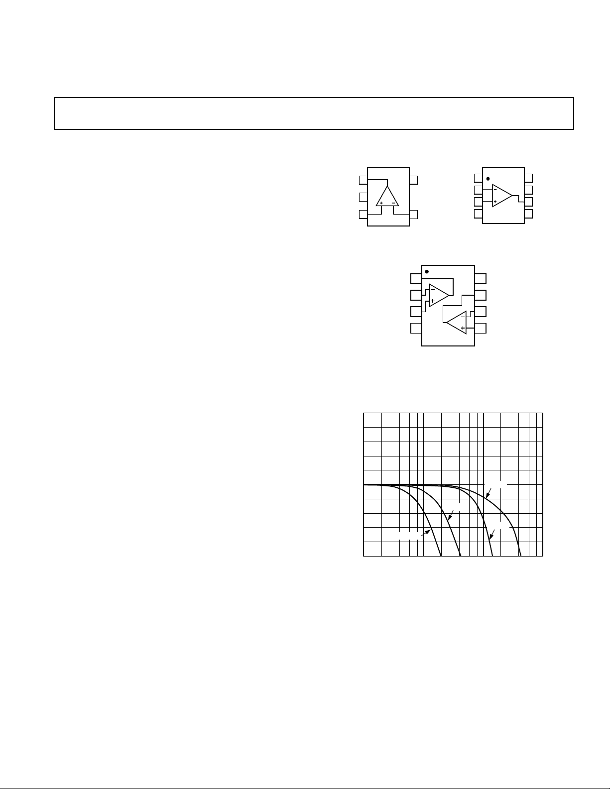
FREQUENCY – MHz
1 100010
GAIN – dB
100
5
4
–5
3
2
1
0
–1
–2
–3
–4
G = +2
G = +10
G = +5
G = +1
+IN
+V
S
–V
S
AD8057
1
2
3
5
4
–IN
V
OUT
(Not to Scale)
8
7
6
5
1
2
3
4
NC
–IN
+IN
NC
+V
S
V
OUT
NC–V
S
AD8057
(Not to Scale)
NC = NO CONNECT
OUT1
–IN1
+IN1
–V
S
+V
S
OUT2
–IN2
+IN2
1
2
3
4
8
7
6
5
(Not to Scale)
AD8058
a
FEATURES
Low Cost Single (AD8057) and Dual (AD8058)
High Speed
325 MHz, –3 dB Bandwidth (G = +1)
1000 V/s Slew Rate
Gain Flatness 0.1 dB to 28 MHz
Low Noise
7 nV/√Hz
Low Power
5.4 mA/Amplifier Typical Supply Current @ +5 V
Low Distortion
–85 dBc @ 5 MHz, R
Wide Supply Range from 3 V to 12 V
Small Packaging
AD8057 Available in SOIC-8 and SOT-23-5
AD8058 Available in SOIC-8 and SOIC
APPLICATIONS
Imaging
DVD/CD
Photodiode Preamp
A-to-D Driver
Professional Cameras
Filters
= 1 k⍀
L
Voltage Feedback, 325 MHz Amplifiers
AD8057/AD8058
CONNECTION DIAGRAMS (TOP VIEWS)
SOT-23-5 (RT-5)
RM-8 (SOIC)
SO-8 (SOIC)
SO-8 (SOIC)
PRODUCT DESCRIPTION
The AD8057 (single) and AD8058 (dual) are very high performance amplifiers with a very low cost. The balance between
cost and performance make them ideal for many applications.
The AD8057 and AD8058 will reduce the need to qualify a
variety of specialty amplifiers.
The AD8057 and AD8058 are voltage feedback amplifiers with
the bandwidth and slew rate normally found in current feedback
amplifiers. The AD8057 and AD8058 are low power amplifiers
having low quiescent current and a wide supply range from 3 V
to 12 V. They have noise and distortion performance required
for high-end video systems as well as dc performance parameters rarely found in high speed amplifiers.
The AD8057 and AD8058 are available in standard SOIC
packaging as well as tiny SOT-23-5 (AD8057) and µSOIC
(AD8058). These amplifiers are available in the industrial tem-
perature range of –40°C to +85°C.
REV. A
Information furnished by Analog Devices is believed to be accurate and
reliable. However, no responsibility is assumed by Analog Devices for its
use, nor for any infringements of patents or other rights of third parties
which may result from its use. No license is granted by implication or
otherwise under any patent or patent rights of Analog Devices.
Figure 1. Small Signal Frequency Response
One Technology Way, P.O. Box 9106, Norwood, MA 02062-9106, U.S.A.
Tel: 781/329-4700 World Wide Web Site: http://www.analog.com
Fax: 781/326-8703 © Analog Devices, Inc., 1999
Page 2

(@ TA = +25ⴗC, VS = ⴞ5 V, RL = 100 ⍀, RF = 0 ⍀, Gain = +1,
AD8057/AD8058–SPECIFICATIONS
unless otherwise noted)
AD8057/AD8058
Parameter Conditions Min Typ Max Units
DYNAMIC PERFORMANCE
–3 dB Bandwidth G = +1, V
G = –1, V
G = +1, V
Bandwidth for 0.1 dB Flatness G = +1, V
Slew Rate G = +1, V
G = +1, V
= 0.2 V p-p 325 MHz
O
= 0.2 V p-p 95 MHz
O
= 2 V p-p 175 MHz
O
= 0.2 V p-p 30 MHz
O
= 2 V Step, R
O
= 4 V Step, R
O
= 2 kΩ 850 V/µs
L
= 2 kΩ 1150 V/µs
L
Settling Time to 0.1% G = +2, VO = 2 V Step 30 ns
NOISE/HARMONIC PERFORMANCE
Total Harmonic Distortion f
SFDR f = 5 MHz, V
Third Order Intercept f = 5 MHz, V
= 5 MHz, VO = 2 V p-p, R
C
= 20 MHz, VO = 2 V p-p, R
f
C
= 2 V p-p, R
O
= ±2.0 V p-p –35 dBm
O
= 1 kΩ –85 dBc
L
= 1 kΩ –62 dBc
L
= 150 Ω –68 dB
L
Crosstalk, Output to Output f = 5␣ MHz, G = +2 –60 dB
Input Voltage Noise f = 100 kHz 7 nV/√Hz
Input Current Noise f = 100 kHz 0.7 pA/√Hz
Differential Gain Error NTSC, G = +2, R
NTSC, G = +2, R
Differential Phase Error NTSC, G = +2, R
NTSC, G = +2, R
= 150 Ω 0.01 %
L
= 1 kΩ 0.02 %
L
= 150 Ω 0.15 Degree
L
= 1 kΩ 0.01 Degree
L
Overload Recovery VIN = 200 mV p-p, G = +1 30 ns
DC PERFORMANCE
Input Offset Voltage 15mV
T
MIN–TMAX
2.5 mV
Input Offset Voltage Drift 3 µV/°C
Input Bias Current 0.5 2.5 µA
T
MIN–TMAX
3.0 µA
Input Offset Current 0.75 ±µA
Open-Loop Gain V
= ±2.5 V, RL = 2 kΩ 50 55 dB
O
V
= ±2.5 V, RL = 150 Ω 50 52 dB
O
INPUT CHARACTERISTICS
Input Resistance 10 MΩ
Input Capacitance +Input 2 pF
Input Common-Mode Voltage Range R
Common-Mode Rejection Ratio V
= 1 kΩ –4.0 +4.0 ±V
L
= ±2.5 V 48 60 dB
CM
OUTPUT CHARACTERISTICS
Output Voltage Swing R
= 2 kΩ –4.0 +4.0 ±V
L
= 150 Ω±3.9 ±V
R
L
Capacitive Load Drive 30% Overshoot 30 pF
POWER SUPPLY
Operating Range ±1.5 ±6.0 ±2.5 V
Quiescent Current for AD8057 6.0 7.5 mA
Quiescent Current for AD8058 14.0 15 mA
Power Supply Rejection Ratio V
Specifications subject to change without notice.
= ±5 V to ±1.5 V 54 59 dB
S
–2– REV. A
Page 3

AD8057/AD8058
SPECIFICATIONS
(@ TA = +25ⴗC, VS = +5 V, RL = 100 ⍀, RF = 0 ⍀, Gain = +1, unless otherwise noted)
AD8057/AD8058
Parameter Conditions Min Typ Max Units
DYNAMIC PERFORMANCE
–3 dB Bandwidth G = +1, V
G = +1, V
Bandwidth for 0.1 dB Flatness V
= 0.2 V p-p 28 MHz
O
Slew Rate G = +1, V
= 0.2 V p-p 300 MHz
O
= 2 V p-p 155 MHz
O
= 2 V Step, R
O
= 2 kΩ 700 V/µs
L
Settling Time to 0.1% G = +2, VO = 2 V Step 35 ns
NOISE/HARMONIC PERFORMANCE
Total Harmonic Distortion f
= 5 MHz, VO = 2 V p-p, R
C
= 20 MHz, VO = 2 V p-p, R
f
C
= 1 kΩ –75 dBc
L
= 1 kΩ –54 dBc
L
Crosstalk, Output to Output f = 5␣ MHz, G = +2 –60 dB
Input Voltage Noise f = 100 kHz 7 nV/√Hz
Input Current Noise f = 100 kHz 0.7 pA/√Hz
Differential Gain Error NTSC, G = +2, R
NTSC, G = +2, R
Differential Phase Error NTSC, G = +2, R
NTSC, G = +2, R
= 150 Ω 0.05 %
L
= 1 kΩ 0.05 %
L
= 150 Ω 0.10 Degree
L
= 1 kΩ 0.02 Degree
L
DC PERFORMANCE
Input Offset Voltage 15mV
T
MIN–TMAX
2.5 mV
Input Offset Voltage Drift 3 µV/°C
Input Bias Current 0.5 2.5 µA
T
MIN–TMAX
3.0 µA
Input Offset Current 0.75 µA
Open-Loop Gain V
= ±1.25 V, RL = 2 kΩ 50 55 dB
O
V
= ±1.25 V, RL = 150 Ω 45 52 dB
O
INPUT CHARACTERISTICS
Input Resistance 10 MΩ
Input Capacitance +Input 2 pF
Input Common-Mode Voltage Range R
Common-Mode Rejection Ratio V
= 1 kΩ 0.9 to 3.4 ±V
L
= ±2.5 V 48 60 dB
CM
OUTPUT CHARACTERISTICS
Output Voltage Swing R
= 2 kΩ 0.9 to 4.1 V
L
= 150 Ω 1.2 to 3.8 V
R
L
Capacitive Load Drive 30% Overshoot 30 pF
POWER SUPPLY
Operating Range 3.0 6.0 10.0 V
Quiescent Current for AD8057 5.4 7.0 mA
Quiescent Current for AD8058 13.5 14 mA
Power Supply Rejection Ratio V
Specifications subject to change without notice.
= ±2.5 V to ±1.5 V 54 58 dB
S
–3–REV. A
Page 4
AD8057/AD8058
WARNING!
ESD SENSITIVE DEVICE
AMBIENT TEMPERATURE – 8C
2.0
1.5
0
–50 80–40
MAXIMUM POWER DISSIPATION – Watts
–30 –20 –10010 20 30 40 50 60 70
1.0
0.5
90
TJ = +1508C
8-LEAD SOIC PACKAGE
mSOIC
SOT-23-5
ABSOLUTE MAXIMUM RATINGS
Supply␣ Voltage . . . . . . . . . . . . . . . . . . . . . . . . . . . . . . . 12.6␣ V
Internal␣ Power␣ Dissipation
2
1
Small␣ Outline␣ Package (R) . . . . . . . . . . . . . . . . . . . . . 0.8␣ W
SOT-23-5 Package . . . . . . . . . . . . . . . . . . . . . . . . . . . 0.5 W
µSOIC Package . . . . . . . . . . . . . . . . . . . . . . . . . . . . . 0.6 W
Input Voltage (Common Mode) . . . . . . . . . . . . . . . . . . . ±V
S
Differential␣ Input␣ Voltage . . . . . . . . . . . . . . . . . . . . . . ±4.0␣ V
Output Short Circuit Duration
. . . . . . . . . . . . . . . . . . . . . . . Observe Power Derating Curves
Storage Temperature Range (R) . . . . . . . . . –65°C to +125°C
Operating Temperature Range (A Grade) . . –40°C to +85°C
Lead Temperature Range (Soldering␣ 10␣ sec) . . . . . . . +300°C
NOTES
1
Stresses above those listed under Absolute Maximum Ratings may cause permanent damage to the device. This is a stress rating only; functional operation of the
device at these or any other conditions above those indicated in the operational
section of this specification is not implied. Exposure to absolute maximum rating
conditions for extended periods may affect device reliability.
2
Specification is for device in free air:
8-Lead SOIC Package: θJA = 160°C/W
5-Lead SOT-23-5 Package: θJA = 240°C/W
8-Lead µSOIC Package: θJA = 200°C/W
MAXIMUM POWER DISSIPATION
The maximum power that can be safely dissipated by the
AD8057/AD8058 is limited by the associated rise in junction
temperature. Exceeding a junction temperature of +175°C for
an extended period can result in device failure. While the
AD8057/AD8058 is internally short circuit protected, this may
not be sufficient to guarantee that the maximum junction tem-
perature (+150°C) is not exceeded under all conditions.
To ensure proper operation, it is necessary to observe the maximum power derating curves.
Figure 2. Plot of Maximum Power Dissipation vs.
Temperature
ORDERING GUIDE
Temperature Package Package
Model Range Descriptions Options Brand Code
AD8057AR –40°C to +85°C 8-Lead Narrow Body SOIC SO-8 Standard
AD8057ACHIPS –40°C to +85°C Die Waffle Pak N/A
AD8057AR-REEL –40°C to +85°C 8-Lead SOIC, 13" Reel SO-8 Standard
AD8057AR-REEL7 –40°C to +85°C 8-Lead SOIC, 7" Reel SO-8 Standard
AD8057ART-REEL –40°C to +85°C 5-Lead SOT-23, 13" Reel RT-5 H7A
AD8057ART-REEL7 –40°C to +85°C 5-Lead SOT-23, 7" Reel RT-5 H7A
AD8058AR –40°C to +85°C 8-Lead Narrow Body SOIC SO-8 Standard
AD8058ACHIPS –40°C to +85°C Die Waffle Pak N/A
AD8058AR-REEL –40°C to +85°C 8-Lead SOIC, 13" Reel SO-8 Standard
AD8058AR-REEL7 –40°C to +85°C 8-Lead SOIC, 7" Reel SO-8 Standard
AD8058ARM –40°C to +85°C 8-Lead µSOIC RM-8 H8A
AD8058ARM-REEL –40°C to +85°C 8-Lead µSOIC, 13" Reel RM-8 H8A
AD8058ARM-REEL7 –40°C to +85°C 8-Lead µSOIC, 7" Reel RM-8 H8A
CAUTION
ESD (electrostatic discharge) sensitive device. Electrostatic charges as high as 4000 V readily
accumulate on the human body and test equipment and can discharge without detection.
Although the AD8057/AD8058 feature proprietary ESD protection circuitry, permanent damage
may occur on devices subjected to high energy electrostatic discharges. Therefore, proper ESD
precautions are recommended to avoid performance degradation or loss of functionality.
–4– REV. A
Page 5
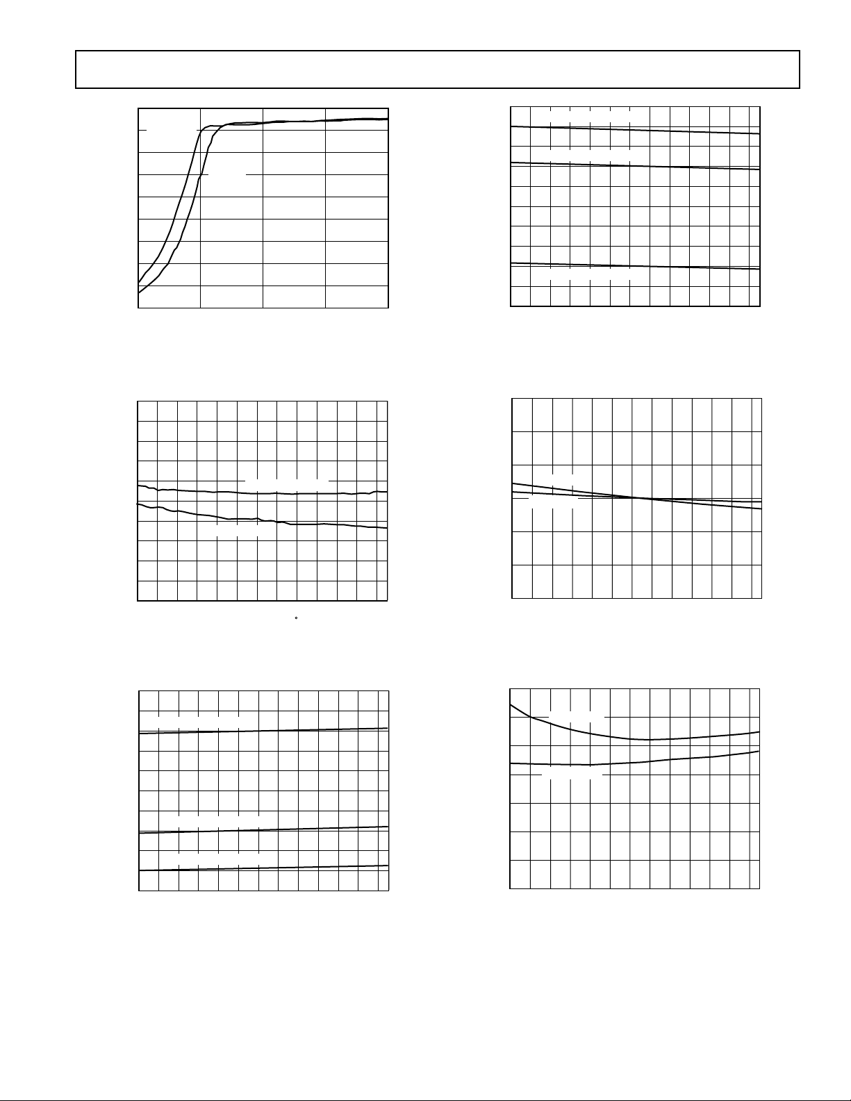
Typical Performance Characteristics–
–4085–30 –20 –10
0
10 20 30 40 50 60 70 80
TEMPERATURE – 8C
0.0
–3.5
–5.0
VOLTS
–0.5
–3.0
–4.0
–4.5
–1.5
–2.5
–1.0
–2.0
–5V SWING RL = 150V
–2.5V SWING RL = 150V
–1.5V SWING RL = 150V
TEMPERATURE – 8C
6
–2
–6
–40 –30
V
OS
– mV
–20 –10
0
10 20 30 40 50 60 70 80
–4
2
0
4
VOS @ 65V
V
OS
@ 61.5V
TEMPERATURE – 8C
3.5
1.5
0
–40 –30
A
VOL
– mV/V
–20 –10
0
10 20 30 40 50 60 70 80
0.5
2.5
2.0
3.0
A
VOL
@ 62.5V
A
VOL
@ 65V
85
1.0
4.5
(+) OUTPUT
4.0
VOLTAGE
3.5
3.0
2.5
2.0
1.5
OUTPUT VOLTAGE
1.0
0.5
0
10 100k100
Figure 3. Output Swing vs. Load Resistance
–3.0
–3.5
–4.0
–4.5
–5.0
– mA
–5.5
SUPPLY
–6.0
–I
–6.5
–7.0
–7.5
–8.0
–4085–30 –20 –10
Figure 4. –I
ABS (–)
OUTPUT
LOAD RESISTANCE – V
–I
SUPPLY
0
SUPPLY
1k 10k
–I
@ 61.5V
SUPPLY
@ 65V
10 20 30 40 50 60 70 80
TEMPERATURE – C
vs. Temperature
AD8057/AD8058
Figure 6. Negative Output Voltage Swing vs.
Temperature
Figure 7. VOS vs. Temperature
5.0
4.5
4.0
3.5
3.0
2.5
VOLTS
2.0
1.5
1.0
0.5
0.0
Figure 5. Positive Output Voltage Swing vs.
Temperature
+5V SWING RL = 150V
+2.5V SWING RL = 150V
+1.5V SWING RL = 150V
–20 –10
–4085–30
10 20 30 40 50 60 70 80
0
TEMPERATURE – 8C
Figure 8. Open-Loop Gain vs. Temperature
–5–REV. A
Page 6

AD8057/AD8058
0.01mF
0.001mF
4.7mF
–V
S
50V
V
IN
HP8130A
PULSE
GENERATOR
TR/TF = 1ns
AD8057/58
0.001mF
0.01mF
4.7mF
1kV
+V
S
V
OUT
100mV
20mV/
DIV
–100mV
4ns/DIV
0.00
–0.10
–0.20
–0.30
–0.40
– mA
B
I
–0.50
–0.60
–0.70
–0.80
–4085–30 –20 –10
Figure 9. Input Bias Current vs. Temperature
4
3
+IB @ 65V
+IB @ 62.5V
–IB @ 65V
–IB @ 61.5V
–Typical Performance Characteristics
–IB @ 62.5V
+IB @ 61.5V
10 20 30 40 50 60 70 80
0
TEMPERATURE –
PSRR @ 61.5V 65V
C
Figure 12. Test Circuit G = +1, RL = 1 kΩ for Figures 13
and 14
PSRR – dB
2
PSRR – mV/V
1
0
–4085–30 –20 –10
10 20 30 40 50 60 70 80
0
TEMPERATURE – C
Figure 10. PSRR vs. Temperature
0
–10
–20
–30
–40
–50
–60
0.1
–PSRR VS = 62.5V
+PSRR VS = 62.5V
Figure 11.±PSRR vs. Frequency
10 100
FREQUENCY – MHz
Figure 13. Small Signal Step Response G = +1, RL = 1 kΩ,
V
= ±5 V
S
5V
1V/DIV
10001
–5V
4ns/DIV
Figure 14. Large Signal Step Response G = +1, RL = 1 kΩ,
V
= ±5.0 V
S
–6– REV. A
Page 7

HP8130A
FREQUENCY – MHz
1 100010
GAIN – dB
100
5
4
–5
3
2
1
0
–1
–2
–3
–4
G = +2
G = +10
G = +5
G = +1
FREQUENCY – MHz
1 100010
GAIN – dB
100
5
4
–5
3
2
1
0
–1
–2
–3
–4
G = +2
G = +10
G = +5
G = +1
FREQUENCY – MHz
1 100010
GAIN – dB
100
5
4
–5
3
2
1
0
–1
–2
–3
–4
G = –2
G = –10
G = –5
G = –1
PULSE
GENERATOR
TR/TF = 1ns
AD8057/AD8058
1kV
+V
S
4.7mF
0.01mF
V
1kV
IN
50V
0.001mF
AD8057/58
0.01mF
0.001mF
–V
S
4.7mF
V
OUT
1kV
Figure 15. Test Circuit G = –1, RL = 1 kΩ for Figures 16
and 17
100mV
20mV/
DIV
0V
–100mV
4ns/DIV
Figure 16. Small Signal Step Response G = –1, RL = 1 k
5V
Figure 18. Small Signal Frequency Response,
V
= 0.2 V p-p
OUT
Ω
Figure 19. Large Signal Frequency Response, V
= 2 V p-p
OUT
1V/DIV
–5V
Figure 17. Large Signal Step Response G = –1, RL = 1 k
4ns/DIV
Ω
Figure 20. Large Signal Frequency Response
–7–REV. A
Page 8

AD8057/AD8058
V
OUT
– V p-p
5.0
4.5
0.0
0
412 3
3.0
1.5
1.0
0.5
4.0
3.5
2.0
2.5
RISE TIME AND FALL TIME – ns
RISE TIME
FALL TIME
V
OUT
– V p-p
5
4
0
0
41
RISE TIME AND FALL TIME – ns
23
3
2
1
RISE TIME
FALL TIME
0.4%
0.3%
0.2%
0.1%
0.0%
–0.1%
–0.2%
–0.3%
–0.4%
0 1020 3040 5060
V
OUT
= –1V TO + 1V OR +1V TO –1V
G = +2
RL = 100V/1kV
TIME – ns
0.5
0.4
0.3
0.2
0.1
0.0
GAIN – dB
–0.1
–0.2
–0.3
–0.4
–0.5
1 100010
FREQUENCY – MHz
100
V
OUT
G = +2
= 1.0kV
R
L
= 1.0kV
R
F
= 0.2V
Figure 21. 0.1 dB Flatness G = +2
–50
–60
–70
–80
–90
DISTORTION – dBc
–100
–110
0.1 1001
THD
2ND
3RD
10
FREQUENCY – MHz
Figure 22. Distortion vs. Frequency, RL = 150
–40
Figure 24. Rise Time and Fall Time vs. V
R
= 1 kΩ, RF = 0
L
Ω
Figure 25. Rise Time and Fall Time vs. V
R
= 100 Ω, RF = 402
L
Ω
Ω
. G = +1,
OUT
. G = +2,
OUT
–50
–60
DISTORTION – dBc
Figure 23. Distortion vs. V
V
–70
–80
S
= ±5.0 V
0.0 4.00.4
20MHz
5MHz
0.8 1.2 1.6 2.0 2.4 2.8 3.2 3.6
V
– V p-p
OUT
@ 20 MHz, 5 MHz, RL = 150Ω,
OUT
Figure 26. Settling Time
–8– REV. A
Page 9

AD8057/AD8058
4.5V
500mV/
DIV
20ns/DIV 37ns
VS = 65.0V
R1 = 1kV
G = +4
FREQUENCY – MHz
0
–20
–120
0.1 1
CROSSTALK – dB
10 100
–60
–80
–100
–40
SIDE B DRIVEN
SIDE A DRIVEN
VS = 62.5V
RL = 1kV
G = +1
2.5V
500mV/
DIV
0V
INPUT SIGNAL
OUTPUT RESPONSE
20ns/DIV
Figure 27. Input Overload Recovery, VS = ±2.5 V
VS = 65.0V
RL = 1kV
G = +1
INPUT SIGNAL 5V
5.0V
1V/DIV
0V
OUTPUT SIGNAL = 4.0V
1.8V
200mV/
DIV
OUTPUT SIGNAL 1.7V
INPUT SIGNAL = 0.6V
20ns/DIV
VS = 62.5V
R1 = 1kV
G = +4
Figure 30. Output Overload Recovery, VS = ±2.5 V
20ns/DIV
Figure 28. Output Overload Recovery, VS = ±5.0 V
0
–10
–20
–30
–40
CMRR – dB
–50
–60
–70
0.1 1001
FREQUENCY – MHz
10
Figure 29. CMRR vs. Frequency
Figure 31. Output Overload Recovery, VS = ±5.0 V
Figure 32. Crosstalk (Output-to-Output) vs. Frequency
–9–REV. A
Page 10

AD8057/AD8058
0.01
–0.05
0.00
–0.01
–0.02
–0.03
–0.04
0.12
0.10
0.08
0.06
0.04
0.02
0.00
0.14
1st 11th6th2nd 7th3rd 8th4th 9th5th 10th
0.00 –0.04–0.01–0.00 –0.01–0.00 –0.01–0.01 –0.02–0.01 –0.03
–0.02
0.00 0.130.090.01 0.110.03 0.120.05 0.120.07 0.13
DIFFERENTIAL PHASE (Degrees)
DIFFERENTIAL GAIN (%)
VS = +5V
R
L
= 150V
VS = +5V
R
L
= 150V
0.01
–0.05
0.00
–0.01
–0.02
–0.03
–0.04
0.12
0.10
0.08
0.06
0.04
0.02
0.00
0.14
1st 11th6th2nd 7th3rd 8th4th 9th5th 10th
0.00 –0.05–0.010.01 –0.02–0.00 –0.02–0.01 –0.03–0.01 –0.04
–0.02
0.00 –0.02–0.00–0.00 –0.000.00 –0.000.00 –0.01–0.00 –0.01
DIFFERENTIAL PHASE (Degrees)
DIFFERENTIAL GAIN (%)
VS = +5V
R
L
= 1kV
VS = +5V
R
L
= 1kV
FREQUENCY – Hz
100
10
0.1
10 100M100
V
NOISE
– nV/ Hz
1k 10k 100k
1
1M 10M
DIFFERENTIAL GAIN (%)
0.00 –0.00–0.00–0.00 –0.000.00 –0.000.00 –0.00–0.00 –0.00
0.015
0.010
0.005
0.000
–0.005
–0.010
–0.015
DIFFERENTIAL PHASE (Degrees)
0.00 0.130.070.00 0.090.02 0.100.03 0.110.05 0.12
0.14
0.12
0.10
0.08
0.06
0.04
0.02
0.00
–0.02
1st 11th6th2nd 7th3rd 8th4th 9th5th 10th
DIFFERENTIAL GAIN (%)
0.00 –0.010.000.00 0.000.00 0.000.01 –0.000.01 –0.01
0.015
0.010
0.005
0.000
–0.005
–0.010
–0.015
DIFFERENTIAL PHASE (Degrees)
0.00 –0.01`–0.000.00 –0.010.00 –0.01–0.00 –0.01–0.00 –0.01
0.14
0.12
0.10
0.08
0.06
0.04
0.02
0.00
–0.02
1st 11th6th2nd 7th3rd 8th4th 9th5th 10th
a.
b.
VS = 65.0V
= 150V
R
L
VS = 65.0V
= 150V
R
L
VS = 65.0V
= 1kV
R
L
VS = 65.0V
= 1kV
R
L
a.
b.
Figure 33. Differential Gain and Differential Phase One
Back Terminated Load (150
180
135
90
45
PHASE – Degrees
0
–45
–90
0.01 10000.1
Figure 34. Open-Loop Gain and Phase vs. Frequency
Ω
) (Video Op Amps Only)
1 10 100
FREQUENCY – MHz
80
60
40
20
OPEN-LOOP GAIN – dB
0
–20
–10– REV. A
Figure 35. Differential Gain and Differential Phase
a. R
= 150Ω, b. RL = 1 k
L
Ω
Figure 36. Voltage Noise vs. Frequency
Page 11

AD8057/AD8058
–2.5V
R
G
50kV
VIN = 200mV p-p
AD8058
0.1mF 10mF
0.1mF
10mF
+2.5V
R
F
C
L
R
S
V
OUT
FET PROBE
100mV
50ns/DIV
200mV
–100mV
–200mV
+ OVERSHOOT
29.0%
100mV
100
10
– pA/ Hz
NOISE
I
1
0.1
10 100M100
1k 10k 100k
FREQUENCY – Hz
1M 10M
Figure 37. Current Noise vs. Frequency
APPLICATIONS
Driving Capacitive Loads
When driving a capacitive load, most op amps will exhibit overshoot in their pulse response.
Figure 39 shows the relationship between the capacitive load that
results in 30% overshoot and closed loop gain of an AD8058. It can
be seen that, under the Gain = +2 condition, the device is stable
with capacitive loads of up to 69 pF.
In general, to minimize peaking or to ensure device stability for
larger values of capacitive loads, a small series resistor, R
be added between the op amp output and the load capacitor, C
, can
S
,
L
as shown in Figure 40.
For the setup shown in Figure 40, the relationship between R
S
and CL was empirically derived and is shown in Table I.
100
10
– V
OUT
Z
1
0.1
0.1 10001
10 100
FREQUENCY – MHz
Figure 38. Output Impedance vs. Frequency
Table I. Recommended Value for Resistors RS, RF, RG vs.
Capacitive Load, C
Gain R
F
, Which Results in 30% Overshoot
L
R
G
CL w/RS = 0 ⍀ CL w/RS = 2.4 ⍀
1 100 11 13
2 100 100 51 69
3 100 50 104 153
4 100 33.2 186 270
5 100 25 245 500
10 100 11 870 1580
500
400
300
– pF
L
C
200
100
0
152
RS = 2.4V
= 0V
R
S
34
CLOSED-LOOP GAIN
Figure 39. Capacitive Load Drive vs. Closed-Loop Gain
Figure 40. Capacitive Load Drive Circuit
Figure 41. Typical Pulse Response with CL = 65 pF,
Gain = +2, and V
= ±2.5 V
S
–11–REV. A
Page 12

AD8057/AD8058
Video Filter
Some composite video signals that are derived from a digital
source contain some clock feedthrough that can cause problems
with downstream circuitry. This clock feedthrough is usually at
27 MHz, which is a standard clock frequency for both NTSC
and PAL video systems. A filter that passes the video band and
rejects frequencies at 27 MHz can be used to remove these
frequencies from the video signal.
Figure 42 shows a circuit that uses an AD8057 to create a single
+5 V supply, three-pole Sallen-Key filter. This circuit uses a
single RC pole in front of a standard two-pole active section. To
shift the dc operating point to midsupply, ac coupling is provided by R4, R5 and C4.
C2
680pF
R
F
1kV
+5V
7
AD8057
4
0.1mF+10mF
6
R1
200V
R2
499V
C1
100pF
R3
49.9V
0.1mF
C3
36pF
+5V
C4
R4
10kV
R5
10kV
2
3
Figure 42. Low-Pass Filter for Video
Figure 43 shows a frequency sweep of this filter. The response is
down 3 dB at 5.7 MHz, so it passes the video band with little
attenuation. The rejection at 27 MHz is 42 dB, which provides
more than a factor of 100 in suppression of the clock components at this frequency.
10
0
–10
–20
–30
–40
–50
–60
LOG MAGNITUDE – dB
–70
–80
–90
100k 100M
1M 10M
FREQUENCY – Hz
Figure 43. Video Filter Response
Differential A-to-D Driver
As system supply voltages are dropping, many A-to-D converters provide differential analog inputs to increase the dynamic
range of the input signal, while still operating on a low supply
voltage. Differential driving can also reduce second and other
even-order distortion products.
Analog Devices offers an assortment of 12- and 14-bit high
speed converters that have differential inputs and can be run
from a single +5 V supply. These include the AD9220, AD9221,
AD9223, AD9224 and AD9225 at 12 bits, and the AD9240,
AD9241, and AD9243 at 14 bits. Although these devices can
operate over a range of common-mode voltages at their analog
inputs, they work best when the common-mode voltage at the
input is at the midsupply or 2.5 V.
Op amp architectures that require upwards of 2 V of headroom
at the output have significant problems when trying to drive
such A-to-Ds while operating with a +5 V positive supply. The
low headroom output design of the AD8057 and AD8058 make
them ideal for driving these types of A-to-D converters.
The AD8058 can be used to make a dc-coupled, single-endedto-differential driver for one of these A-to-Ds. Figure 44 is a
schematic of such a circuit for driving an AD9225, a 12-bit,
25 MSPS A-to-D converter.
1kV
+5V
+
10mF
0.1mF
3
AD8058
2
6
AD8058
5
8
–5V
+
10mF
50V
50V
1
1kV
1kV
7
4
0.1mF
1kV
1kV
V
IN
0V
1kV
1kV
1kV
0.1mF
VINA
VINB
+2.5V
+
10mF
AD9225
+5V
REF
Figure 44. Schematic Circuit for Driving AD9225
In this circuit, one of the op amps is configured in the inverting
mode, while the other is in the noninverting mode. However, to
provide better bandwidth matching, each op amp is configured
for a noise gain of 2. The inverting op amp is configured for a
gain of –1, while the noninverting op amp is configured for a
gain of +2. Each of these produces a noise gain of 2, which is
only determined by the inverse of the feedback ratio. The input
signal to the noninverting op amp is divided by 2 in order to
normalize its level and make it equal to the inverting output.
–12– REV. A
Page 13

AD8057/AD8058
For zero volts input, the outputs of the op amps want to be at
2.5 V, which is the midsupply level of the A-to-D. This is accomplished by first taking the 2.5 V reference output of the
A-to-D and dividing it by two by a pair of 1 kΩ resistors. The
resulting 1.25 V is applied to each op amp’s positive input. This
voltage is then multiplied by the gain of 2 of the op amps to
provide a 2.5 V level at each output.
The assumption for this circuit is that the input signal is bipolar
with respect to round and the circuit must be dc coupled. This
implies the existence of a negative supply elsewhere in the system.
This circuit uses –5 V as the negative supply for the AD8058.
If the AD8058 negative supply were tied to ground, there would
be a problem at the input of the noninverting op amp. The
input common-mode voltage can only go to within 1 V of the
negative rail. Since this circuit requires that the positive inputs
operate with a 1.25 V bias, there is not enough room to swing
this voltage in the negative direction. The inverting stage does
not have this problem, because its common-mode input voltage
remains fixed at 1.25 V. If dc-coupling is not required, various
ac-coupling techniques can be used to eliminate this problem.
Layout
The AD8057 and AD8058 are high speed op amps and should
be used in a board layout that follows standard high speed design rules. All the signal traces should be as short and direct as
possible. In particular, the parasitic capacitance on the inverting
input of each device should be kept to a minimum to avoid
excessive peaking and other undesirable performance.
The power supplies should be bypassed very close to the power
pins of the package with 0.1 µF in parallel with a larger, approxi-
mately 10 µF tantalum capacitor. These capacitors should be
connected to a ground plane that is either on an inner layer, or
fills the area of the board that is not used for other signals.
–13–REV. A
Page 14

AD8057/AD8058
0.1968 (5.00)
0.1890 (4.80)
8
5
41
0.2440 (6.20)
0.2284 (5.80)
PIN 1
0.1574 (4.00)
0.1497 (3.80)
0.0688 (1.75)
0.0532 (1.35)
SEATING
PLANE
0.0098 (0.25)
0.0040 (0.10)
0.0192 (0.49)
0.0138 (0.35)
0.0500
(1.27)
BSC
0.0098 (0.25)
0.0075 (0.19)
0.0500 (1.27)
0.0160 (0.41)
8°
0°
0.0196 (0.50)
0.0099 (0.25)
x 45°
OUTLINE DIMENSIONS
Dimensions shown in inches and (mm).
0.122 (3.10)
0.114 (2.90)
0.006 (0.15)
0.002 (0.05)
SEATING
0.122 (3.10)
0.114 (2.90)
8
1
PIN 1
0.0256 (0.65) BSC
0.120 (3.05)
0.112 (2.84)
0.018 (0.46)
0.008 (0.20)
PLANE
8-Lead SOIC
(RM-8)
5
0.199 (5.05)
0.187 (4.75)
4
0.043 (1.09)
0.037 (0.94)
0.011 (0.28)
0.003 (0.08)
0.120 (3.05)
0.112 (2.84)
338
278
0.028 (0.71)
0.016 (0.41)
5-Lead Surface Mount (SOT-23)
(RT-5)
0.1181 (3.00)
0.1102 (2.80)
8-Lead Narrow Body SOIC
(SO-8)
C3388a–0–9/99
0.0669 (1.70)
0.0590 (1.50)
0.0512 (1.30)
0.0354 (0.90)
0.0059 (0.15)
0.0019 (0.05)
PIN 1
1 3
2
0.0748 (1.90)
BSC
0.0197 (0.50)
0.0138 (0.35)
4 5
0.1181 (3.00)
0.1024 (2.60)
0.0374 (0.95) BSC
0.0571 (1.45)
0.0374 (0.95)
SEATING
PLANE
10°
0°
0.0079 (0.20)
0.0031 (0.08)
0.0217 (0.55)
0.0138 (0.35)
PRINTED IN U.S.A.
–14– REV. A
 Loading...