

Datasheet AD8055ART-REEL7, AD8055ART-REEL, AD8055AR-REEL7, AD8055AR-REEL, AD8055AR Datasheet (Analog Devices)
...Page 1
Low Cost, 300 MHz
1
2
3
4
8
7
6
5
(Not to Scale)
AD8055
–IN
–V
S
+IN
+V
S
V
OUT
NC
NC
NC
NC = NO CONNECT
a
FEATURES
Low Cost Single (AD8055) and Dual (AD8056)
Easy to Use Voltage Feedback Architecture
High Speed
300 MHz, –3 dB Bandwidth (G = +1)
1400 V/s Slew Rate
20 ns Settling to 0.1%
Low Distortion: –72 dBc @ 10 MHz
Low Noise: 6 nV/√Hz
Low DC Errors: 5 mV Max V
Small Packaging
AD8055 Available in SOT-23-5
AD8056 Available in 8-Lead microSOIC
Excellent Video Specifications (R
Gain Flatness 0.1 dB to 40 MHz
0.01% Differential Gain Error
0.02ⴗ Differential Phase Error
Drives Four Video Loads (37.5 ⍀) with 0.02% and
0.1ⴗ Differential Gain and Differential Phase
Low Power, ⴞ5 V Supplies
5 mA Typ/Amplifier Power Supply Current
High Output Drive Current: Over 60 mA
APPLICATIONS
Imaging
Photodiode Preamp
Video Line Driver
Differential Line Driver
Professional Cameras
Video Switchers
Special Effects
A-to-D Driver
Active Filters
PRODUCT DESCRIPTION
The AD8055 (single) and AD8056 (dual) voltage feedback
amplifiers offer bandwidth and slew rate typically found in
current feedback amplifiers. Additionally, these amplifiers are
easy to use and available at a very low cost.
Despite their low cost, the AD8055 and AD8056 provide excellent
overall performance. For video applications, their differential gain
and phase error are 0.01% and 0.02° into a 150 Ω load, and
0.02% and 0.1° while driving four video loads (37.5 Ω). Their
0.1 dB flatness out to 40 MHz, wide bandwidth out to 300 MHz,
along with 1400 V/µs slew rate and 20 ns settling time, make
them useful for a variety of high-speed applications.
, 1.2 A Max I
OS
= 150 ⍀, G = +2)
L
B
Voltage Feedback Amplifiers
AD8055/AD8056
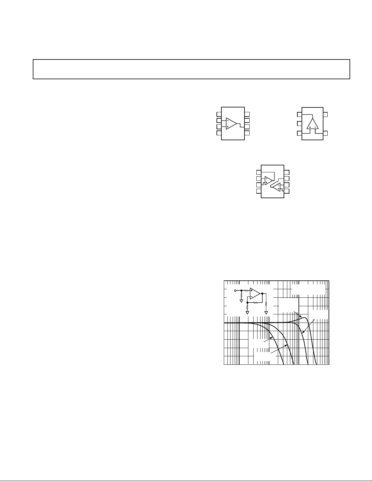
FUNCTIONAL BLOCK DIAGRAMS
N-8 and R-8
N-8, R-8, microSOIC (RM)
AD8056
1
OUT1
2
–IN1
3
+IN1
4
–V
S
(Not to Scale)
The AD8055 and AD8056 require only 5 mA typ/amplifier of
supply current and operate on dual ±5 V or single +12 V power
supply, while being capable of delivering over 60 mA of load
current. All this is offered in a small 8-lead plastic DIP, 8-lead
SOIC packages, 5-lead SOT-23-5 package (AD8055) and an
8-lead microSOIC package (AD8056). These features make
the AD8055/AD8056 ideal for portable and battery powered
applications where size and power are critical. These amplifiers are
available in the industrial temperature range of –40°C to +85°C.
5
R
4
3
2
1
0
GAIN – dB
–1
–2
–3
–4
–5
0.3M 1G
C
V
IN
50⍀
R
S
1M 10M 100M
R
F
G = +10
= 909⍀
R
F
G = +5
= 1000⍀
R
F
FREQUENCY – Hz
V
OUT
R
L
Figure 1. Frequency Response
SOT-23-5 (RT)
1
V
OUT
–V
2
S
3
+IN
+V
8
S
7
OUT
–IN2
6
+IN2
5
V
OUT
RL = 100⍀
G = +1
= 0⍀
R
F
= 100⍀
R
C
AD8055
(Not to Scale)
= 100mV p-p
G = +2
= 402⍀
R
F
+V
5
S
–IN
4
REV. E
Information furnished by Analog Devices is believed to be accurate and
reliable. However, no responsibility is assumed by Analog Devices for its
use, nor for any infringements of patents or other rights of third parties that
may result from its use. No license is granted by implication or otherwise
under any patent or patent rights of Analog Devices.
One Technology Way, P.O. Box 9106, Norwood, MA 02062-9106, U.S.A.
Tel: 781/329-4700 www.analog.com
Fax: 781/326-8703 © Analog Devices, Inc., 2001
Page 2

(@ TA = 25ⴗC, VS = ⴞ5 V, RF = 402 ⍀, RL = 100 ⍀, Gain = +2,
AD8055/AD8056–SPECIFICATIONS
unless otherwise noted)
Model AD8055A/AD8056A
Conditions Min Typ Max Unit
DYNAMIC PERFORMANCE
–3 dB Bandwidth G = +1, V
G = +1, V
G = +2, V
G = +2, V
Bandwidth for 0.1 dB Flatness V
= 100 mV p-p 25 40 MHz
O
Slew Rate G = +1, V
G = +2, V
Settling Time to 0.1% G = +2, V
Rise and Fall Time, 10% to 90% G = +1, V
G = +1, V
G = +2, V
= 0.1 V p-p 220 300 MHz
O
= 2 V p-p 125 150 MHz
O
= 0.1 V p-p 120 160 MHz
O
= 2 V p-p 125 150 MHz
O
= 4 V Step 1000 1400 V/µs
O
= 4 V Step 750 840 V/µs
O
= 2 V Step 20 ns
O
= 0.5 V Step 2 ns
O
= 4 V Step 2.7 ns
O
= 0.5 V Step 2.8 ns
O
G = +2, VO = 4 V Step 4 ns
NOISE/HARMONIC PERFORMANCE
Total Harmonic Distortion fC = 10 MHz, VO = 2 V p-p, RL = 1 kΩ –72 dBc
= 20 MHz, VO = 2 V p-p, RL = 1 kΩ –57 dBc
f
C
Crosstalk, Output to Output (AD8056) f = 5 MHz, G = +2 –60 dB
Input Voltage Noise f = 100 kHz 6 nV/√Hz
Input Current Noise f = 100 kHz 1 pA/√Hz
Differential Gain Error NTSC, G = +2, R
NTSC, G = +2, R
Differential Phase Error NTSC, G = +2, R
= 150 Ω 0.01 %
L
= 37.5 Ω 0.02 %
L
= 150 Ω 0.02 Degree
L
NTSC, G = +2, RL = 37.5 Ω 0.1 Degree
DC PERFORMANCE
Input Offset Voltage 35 mV
T
MIN–TMAX
10 mV
Offset Drift 6 µV/°C
Input Bias Current 0.4 1.2 µA
1 µA
Open Loop Gain V
T
MIN–TMAX
= ±2.5 V 66 71 dB
O
T
MIN–TMAX
64 dB
INPUT CHARACTERISTICS
Input Resistance 10 MΩ
Input Capacitance 2pF
Input Common-Mode Voltage Range 3.2 ±V
Common-Mode Rejection Ratio VCM = ±2.5 V 82 dB
OUTPUT CHARACTERISTICS
Output Voltage Swing RL = 150 Ω 2.9 3.1 ±V
Output Current
Short Circuit Current
1
1
VO = ±2.0 V 55 60 mA
110 mA
POWER SUPPLY
Operating Range ±4.0 ±5.0 ±6.0 V
Quiescent Current AD8055 5.4 6.5 mA
T
MIN–TMAX
7.3 mA
AD8056 10 12 mA
T
Power Supply Rejection Ratio +V
MIN–TMAX
= +5 V to +6 V, –VS = –5 V 66 72 dB
S
13.3 mA
–VS = –5 V to –6 V, +VS = +5 V 69 86 dB
OPERATING TEMPERATURE RANGE –40 +85 °C
NOTES
1
Output current is limited by the maximum power dissipation in the package. See the power derating curves.
Specifications subject to change without notice.
–2–
REV. E
Page 3
AD8055/AD8056
WARNING!
ESD SENSITIVE DEVICE
ABSOLUTE MAXIMUM RATINGS
Supply Voltage . . . . . . . . . . . . . . . . . . . . . . . . . . . . . . . 13.2 V
Internal Power Dissipation
2
1
Plastic DIP Package (N) . . . . . . . . . . . . . . . . . . . . . . 1.3 W
Small Outline Package (R) . . . . . . . . . . . . . . . . . . . . . 0.8 W
SOT-23-5 Package (RT) . . . . . . . . . . . . . . . . . . . . . . 0.5 W
microSOIC Package (RM) . . . . . . . . . . . . . . . . . . . . . 0.6 W
Input Voltage (Common Mode) . . . . . . . . . . . . . . . . . . . ± V
S
Differential Input Voltage . . . . . . . . . . . . . . . . . . . . . . ±2.5 V
Output Short Circuit Duration
. . . . . . . . . . . . . . . . . . . . . . Observe Power Derating Curves
Storage Temperature Range N, R . . . . . . . . –65°C to +125°C
Operating Temperature Range (A Grade) . . –40°C to +85°C
Lead Temperature Range (Soldering 10 sec) . . . . . . . . 300°C
NOTES
1
Stresses above those listed under Absolute Maximum Ratings may cause permanent
damage to the device. This is a stress rating only; functional operation of the device at
these or any other conditions above those indicated in the operational section of this
specification is not implied. Exposure to absolute maximum rating conditions for
extended periods may affect device reliability.
2
Specification is for device in free air:
8-Lead Plastic DIP Package: θJA = 90°C/W
8-Lead SOIC Package: θJA = 155°C/W
5-Lead SOT-23-5 Package: θJA = 240°C/W
8-Lead microSOIC Package: θJA = 200°C/W
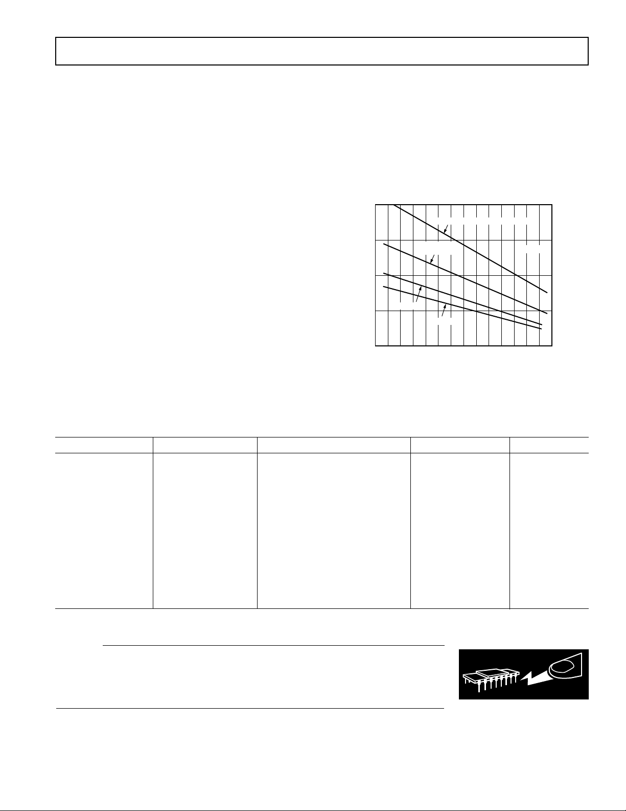
MAXIMUM POWER DISSIPATION
The maximum power that can be safely dissipated by the AD8055/
AD8056 is limited by the associated rise in junction temperature.
The maximum safe junction temperature for plastic encapsulated
devices is determined by the glass transition temperature of the
plastic, approximately 150°C. Exceeding this limit temporarily
may cause a shift in parametric performance due to a change in
the stresses exerted on the die by the package. Exceeding a
junction temperature of 175°C for an extended period can result
in device failure.
While the AD8055/AD8056 are internally short circuit protected,
this may not be sufficient to guarantee that the maximum junction
temperature (150°C) is not exceeded under all conditions. To
ensure proper operation, it is necessary to observe the maximum
power derating curves.
2.0
8-LEAD PLASTIC DIP PACKAGE
1.5
1.0
0.5
MAXIMUM POWER DISSIPATION – Watts
0
–40 –30 –20 –100 102030405060 708090
–50
8-LEAD SOIC
PACKAGE
SOIC
SOT-23-5
AMBIENT TEMPERATURE – ⴗC
TJ = 150ⴗC
Figure 2. Plot of Maximum Power Dissipation vs.
Temperature for AD8055/AD8056
ORDERING GUIDE
Model Temperature Range Package Description Package Option Branding Code
AD8055AN –40°C to +85°C Plastic DIP N-8
AD8055AR –40°C to +85°C Small Outline Package (SOIC) SO-8
AD8055AR-REEL –40°C to +85°C 13" Tape and Reel SO-8
AD8055AR-REEL7 –40°C to +85°C 7" Tape and Reel SO-8
AD8055ART-REEL –40°C to +85°C 13" Tape and Reel RT-5 H3A
AD8055ART-REEL7 –40°C to +85°C 7" Tape and Reel RT-5 H3A
AD8056AN –40°C to +85°C Plastic DIP N-8
AD8056AR –40°C to +85°C Small Outline Package (SOIC) SO-8
AD8056AR-REEL –40°C to +85°C 13" Tape and Reel SO-8
AD8056AR-REEL7 –40°C to +85°C 7" Tape and Reel SO-8
AD8056ARM –40°C to +85°C microSOIC RM-8 H5A
AD8056ARM-REEL –40°C to +85°C 13" Tape and Reel RM-8 H5A
AD8056ARM-REEL7 –40°C to +85°C 7" Tape and Reel RM-8 H5A
CAUTION
ESD (electrostatic discharge) sensitive device. Electrostatic charges as high as 4000 V readily
accumulate on the human body and test equipment and can discharge without detection.
Although the AD8055/AD8056 features proprietary ESD protection circuitry, permanent damage may occur on devices subjected to high-energy electrostatic discharges. Therefore, proper
ESD precautions are recommended to avoid performance degradation or loss of functionality.
REV. E
–3–
Page 4
AD8055/AD8056
–Typical Performance Characteristics
+V
HP8130A
PULSE
GENERATOR
= 1ns
T
R/TF
V
100⍀
IN
50⍀
3
AD8055
2
7
4
–V
TPC 1. Test Circuit, G = +1, RL = 100
2
AD8055
3
402⍀
+V
4.7F
S
0.01F
0.001F
7
6
V
OUT
4
4.7F
0.01F
0.001F
–V
S
100⍀
Ω
4.7F
S
0.01F
0.001F
V
4.7F
OUT
100⍀
6
0.01F
0.001F
S
Ω
HP8130A
PULSE
GENERATOR
= 0.67ns
T
R/TF
V
402⍀
IN
57⍀
TPC 4. Test Circuit, G = –1, RL = 100
TPC 2. Small Step Response, G = +1
TPC 3. Large Step Response, G = +1
TPC 5. Small Step Response, G = –1
TPC 6. Large Step Response, G = –1
–4–
REV. E
Page 5

AD8055/AD8056
FREQUENCY – Hz
10k
10M100k 1M
V
OUT
= 2V p-p
G = +2
R
L
= 100⍀
2ND
3RD
–50
–100
–60
–70
–80
–90
100M
HARMONIC DISTORTION – dBc
FREQUENCY – Hz
10k
10M100k 1M
V
OUT
= 2V p-p
G = +2
R
L
= 1k⍀
2ND
3RD
–50
–100
–60
–70
–80
–90
100M
DISTORTION – dBc
5
4
3
2
1
0
GAIN – dB
–1
–2
–3
–4
–5
0.3M 1G
R
C
V
IN
50⍀
R
S
1M 10M 100M
R
F
G = +10
= 909⍀
R
F
G = +5
= 1000⍀
R
F
FREQUENCY – Hz
V
OUT
R
L
V
R
OUT
= 100⍀
L
G = +2
R
F
= 100mV p-p
= 402⍀
G = +1
= 0⍀
R
F
= 100⍀
R
C
TPC 7. Small Signal Frequency Response,
G = +1, G = +2, G = +5, G = +10
5
4
3
2
1
0
GAIN – dB
–1
–2
–3
–4
–5
0.3M 1G
G = +10
= 909⍀
R
F
G = +5
= 1000⍀
R
F
1M 10M 100M
FREQUENCY – Hz
G = +2
= 402⍀
R
F
V
R
OUT
= 100⍀
L
= 2V p-p
G = +1
= 0⍀
R
F
TPC 8. Large Signal Frequency Response,
G = +1, G = +2, G = +5, G = +10
TPC 10. Distortion vs. Frequency
TPC 11. Distortion vs. Frequency
REV. E
0.5
0.4
0.3
0.2
0.1
0
–0.1
OUTPUT – dB
–0.2
–0.3
–0.4
–0.5
0.3M
FREQUENCY – Hz
TPC 9. 0.1 dB Flatness
V
= 100mV
OUT
G = +2
RL = 100⍀
RF = 402⍀
–40
G = +2
–50
R
= 1k⍀
L
–60
–70
DISTORTION – dBc
–80
–90
1G1M 10M 100M
0 1.20.4 0.8
TPC 12. Distortion vs. V
2ND
3RD
1.6
2.0 2.4 2.8 3.2 3.6 4.0
V
– V p-p
OUT
@ 20 MHz
OUT
–5–
Page 6

AD8055/AD8056
10
G = +1
R
= 100⍀
9
L
R
= 0⍀
F
8
7
6
5
4
3
RISETIME AND FALLTIME – ns
2
1
0
05.00.5 1.0 1.5 2.0 2.5 3.0 3.5 4.0 4.5
FALLTIME
RISETIME
VIN – V p-p
TPC 13. Risetime and Falltime vs. V
10
G = +1
9
= 1k⍀
R
L
R
= 0⍀
F
8
7
6
5
4
3
RISETIME AND FALLTIME – ns
2
1
0
0 5.00.5 1.0 1.5 2.0 2.5 3.0 3.5 4.0 4.5
FALLTIME
RISETIME
VIN – V p-p
TPC 14. Risetime and Falltime vs. V
10
G = +2
9
= 100⍀
R
L
8
R
= 402⍀
F
7
6
5
4
3
RISETIME AND FALLTIME – ns
2
1
0
0 0.2 0.4 0.6 0.8 1.0 1.2 1.4 1.6
IN
IN
TPC 16. Risetime and Falltime vs. V
5.0
G = +2
4.5
= 1k⍀
R
L
R
= 402⍀
F
4.0
3.5
3.0
2.5
2.0
1.5
RISETIME AND FALLTIME – ns
1.0
0.5
0
0 0.2 0.4 0.6 0.8 1.0 1.2 1.4 1.6
TPC 17. Risetime and Falltime vs. V
RISETIME
FALLTIME
VIN – V p-p
IN
RISETIME
FALLTIME
VIN – V p-p
IN
–0.1
SETTLING TIME – %
–0.2
–0.3
–0.4
–0.5
0.7
0.6
0.5
0.4
0.3
0.2
0.1
0
02010
V
= 0V TO +2V OR
OUT
= 0V TO –2V
V
OUT
G = +2
= 100⍀
R
L
30
TIME – ns
40 50 60
TPC 15. Settling Time
–6–
PSRR – dB
–10
–20
–30
–40
–50
–60
–70
–80
–90
10
G = +2
0
R
= 402⍀
F
–PSRR
+PSRR
0.1
FREQUENCY – MHz
5001 10 100
TPC 18. PSRR vs. Frequency
REV. E
Page 7

AD8055/AD8056
TPC 19. Overload Recovery
–20
VIN = 0dBm
–30
G = +2
= 100⍀
R
L
–40
= 402⍀
R
F
–50
–60
–70
–80
CROSSTALK – dB
–90
–100
–110
–120
0.1
SIDE 2 DRIVEN
SIDE 1 DRIVEN
FREQUENCY – MHz
TPC 20. Crosstalk (Output-to-Output) vs. Frequency
0
402⍀
–10
–20
–30
–40
–50
CMRR – dB
–60
–70
–80
–90
–100
0.1
402⍀
402⍀
58⍀ 402⍀
50⍀
FREQUENCY – MHz
TPC 22. Overload Recovery
90
80
70
60
50
40
30
20
OPEN LOOP GAIN – dB
10
0
2001 10 100
–10
0.01
0.1 1 10 100 500
FREQUENCY – MHz
RL = 100⍀
TPC 23. Open Loop Gain vs. Frequency
180
135
90
45
PHASE – Degrees
0
–45
–90
5001 10 100
10k
100k 1M 10M 100M 500M
FREQUENCY – Hz
REV. E
TPC 21. CMRR vs. Frequency
TPC 24. Phase vs. Frequency
–7–
Page 8

AD8055/AD8056
0.04
0.02
0.00
G = +2
–0.02
R
–0.04
1ST 2ND 3RD 4TH 5TH 6TH 7TH 8TH 9TH 10TH 11TH
DIFFERENTIAL GAIN – %
0.04
0.02
0.00
Degrees
–0.02
–0.04
DIFFERENTIAL PHASE –
1ST 2ND 3RD 4TH 5TH 6TH 7TH 8TH 9TH 10TH 11TH
1 BACK TERMINATED LOAD (150⍀)
= 402⍀
F
1 BACK TERMINATED LOAD (150⍀)
G = +2
R
= 402⍀
F
IRE
IRE
TPC 25. Differential Gain and Differential Phase
0.04
0.02
0.00
G = +2
–0.02
R
= 402⍀
F
–0.04
1ST 2ND 3RD 4TH 5TH 6TH 7TH 8TH 9TH 10TH 11TH
DIFFERENTIAL GAIN – %
0.15
0.10
0.05
0.00
–0.05
Degrees
G = +2
–0.10
R
= 402⍀
F
–0.15
DIFFERENTIAL PHASE –
1ST 2ND 3RD 4TH 5TH 6TH 7TH 8TH 9TH 10TH 11TH
4 VIDEO LOADS (37.5⍀)
IRE
4 VIDEO LOADS (37.5⍀)
IRE
TPC 26. Differential Gain and Differential Phase
1000
100
10
VOLTAGE NOISE – nV Hz
1
10 15M100
6nV/ Hz
1k 10k 100k 1M 10M
FREQUENCY – Hz
TPC 28. Voltage Noise vs. Frequency
100
10
1
VOLTAGE NOISE – pA Hz
0.1
10 15M100
1k 10k 100k 1M 10M
FREQUENCY – Hz
TPC 29. Current Noise vs. Frequency
5.0
4.5
4.0
3.5
3.0
– Volts
2.5
OUT
2.0
ⴞV
1.5
1.0
0.5
0
–55 5–35 –15
RL = 1k⍀
RL = 150⍀
25 45 65 85 105 125
TEMPERATURE – ⴗC
RL = 50⍀
TPC 27. Output Swing vs. Temperature
VS = ⴞ5V
–8–
45
G = +2
40
35
30
25
| – ⍀
20
OUT
15
|Z
10
–5
5
0
0.01
= 402⍀
R
F
0.1 1 10 100
FREQUENCY – MHz
TPC 30. Output Impedance vs. Frequency
500
REV. E
Page 9

AD8055/AD8056
75⍀
R
I
402⍀
+5V
R
F
402⍀
–5V
AD8056
402⍀
402⍀
402⍀
49.9⍀
49.9⍀
V
IN
+V
OUT
402⍀
–V
OUT
10F
0.1F
1
2
3
8
AMP1
5
6
7
4
AMP2
10F
0.1F
APPLICATIONS
Four-Line Video Driver
The AD8055 is a useful low cost circuit for driving up to four
video lines. For such an application, the amplifier is configured
for a noninverting gain of 2 as shown in Figure 3. The input
video source is terminated in 75 Ω and applied to the high
The gain of this circuit from the input to Amp 1 output is R
while the gain to the output of Amp 2 is –R
. The circuit thus
F/RI
creates a balanced differential output signal from a single-ended
input. The advantage of this circuit is that the gain can be changed
by changing a single resistor and still maintain the balanced
differential outputs.
F/RI
,
impedance noninverting input.
Each output cable is connected to the op amp output via a 75 Ω
series back termination resistor for proper cable termination.
The terminating resistors at the other ends of the lines will
divide the output signal by two, which is compensated for by
the gain-of-two of the op amp stage.
For a single load, the differential gain error of this circuit was
measured to be 0.01%, with a differential phase error of
0.02 degrees. The two load measurements were 0.02% and
0.03 degrees, respectively. For four loads, the differential
gain error is 0.02%, while the differential phase increases to
0.1 degrees.
+5V
402⍀
402⍀
0.1F
2
7
AD8055
3
V
IN
75⍀
4
0.1F
10F
6
10F
75⍀
75⍀
75⍀
75⍀
75⍀
75⍀
V
V
V
OUT1
OUT2
OUT3
Figure 4. Single-Ended to Differential Line Driver
–5V
75⍀
75⍀
V
OUT4
Low Noise, Low Power Preamp
The AD8055 makes a good, low cost, low noise, low power
preamp. A gain of 10 preamp can be made with a feedback
Figure 3. Four-Line Video Driver
resistor of 909 Ω and a gain resistor of 100 Ω as shown in
Figure 5. The circuit has a –3 dB bandwidth of 20 MHz.
Single-Ended to Differential Line Driver
Creating differential signals from single-ended signals is required
for driving balanced, twisted pair cables, differential input A/D
909⍀
+5V
converters and other applications that require differential signals.
This is sometimes accomplished by using an inverting and a noninverting amplifier stage to create the complementary signals.
The circuit shown in Figure 4 shows how an AD8056 can be
used to make a single-ended to differential converter that offers
some advantages over the architecture mentioned above. Each op
amp is configured for unity gain by the feedback resistors from the
outputs to the inverting inputs. In addition, each output drives the
opposite op amp with a gain of –1 by means of the crossed
resistors. The result of this is that the outputs are complementary
and there is high gain in the overall configuration.
Feedback techniques similar to a conventional op amp are used
to control the gain of the circuit. From the noninverting input
of Amp 1 to the output of Amp 2, is an inverting gain. Between
these points a feedback resistor can be used to close the loop.
As in the case of a conventional op amp inverting gain stage, an
input resistor is added to vary the gain.
Figure 5. Low Noise, Low Power Preamp with G = +10
and BW = 20 MHz
With a low source resistance (<approximately 100 Ω), the major
contributors to the input referred noise of this circuit are the
input voltage noise of the amplifier and the noise of the 100 Ω
resistor. These are 6 nV/√Hz and 1.2 nV/√Hz, respectively. These
values yield a total input referred noise of 6.1 nV/√Hz.
100⍀
R
S
2
3
0.1F10F
7
AD8055
4
0.1F
–5V
+
6
10F
V
OUT
REV. E
–9–
Page 10

AD8055/AD8056
Power Dissipation Limits
With a 10 V supply (total VCC – VEE), the quiescent power
dissipation of the AD8055 in the SOT-23-5 package is 65 mW,
while the quiescent power dissipation of the AD8056 in the
microSOIC is 120 mW. This translates into a 15.6°C rise above
the ambient for the SOT-23-5 package and a 24°C rise for the
microSOIC package.
The power dissipated under heavy load conditions is approximately equal to the supply voltage minus the output voltage,
times the load current, plus the quiescent power computed above.
This total power dissipation is then multiplied by the thermal
resistance of the package to find the temperature rise, above
ambient, of the part. The junction temperature should be kept
below 150°C.
The AD8055 in the SOT-23-5 package can dissipate 270 mW
while the AD8056 in the microSOIC package can dissipate
325 mW (at 85°C ambient) without exceeding the maximum
die temperature. In the case of the AD8056, this is greater than
1.5 V rms into 50 Ω, enough to accommodate a 4 V p-p sine-wave
signal on both outputs simultaneously. But since each output of
the AD8055 or AD8056 is capable of supplying as much as
110 mA into a short circuit, a continuous short circuit condition
will exceed the maximum safe junction temperature.
Resistor Selection
The following table is provided as a guide to resistor selection
for maintaining gain flatness vs. frequency for various values
of gain.
–3 dB
Bandwidth
Gain RF (⍀)R
(⍀) (MHz)
I
+1 0 — 300
+2 402 402 160
+5 1k 249 45
+10 909 100 20
Driving Capacitive Loads
When driving a capacitive load, most op amps will exhibit peaking
in the frequency response just before the frequency rolls off. Figure
6 shows the responses for an AD8056 running at a gain of +2,
with a 100 Ω load that is shunted by various values of capacitance.
It can be seen that under these conditions, the part is still stable
with capacitive loads of up to 30 pF.
5
4
3
= 0dBm
V
IN
2
1
0
–1
–2
NORMALIZED GAIN – dB
–3
–4
–5
0.3 5001 10 100
402⍀
402⍀
C
L
50⍀
FREQUENCY – MHz
CL = 30pF
100⍀
CL = 20pF
CL = 10pF
CL = 0pF
Figure 6. Capacitive Load Drive
In general, to minimize peaking or to ensure the stability for
larger values of capacitive loads, a small series resistor, R
be added between the op amp output and the capacitor, C
the setup depicted in Figure 7, the relationship between R
was empirically derived and is shown in Figure 8. RS was
C
L
S,
can
. For
L
and
S
chosen to produce less than 1 dB of peaking in the frequency
response. Note also that after a sharp rise R
quickly settles to
S
about 25 Ω.
402⍀
+5V
7
4
–5V
0.1F 10F
6
0.1F
10F
R
S
L
FET PROBE
V
OUT
C
L
VIN = 0dBm
40
35
30
25
– ⍀
20
S
R
15
402⍀
2
AD8055
3
50⍀
Figure 7. Setup for RS vs. C
–10–
10
5
0
0 27010 20 30 40 50 60
Figure 8. RS vs. C
CL – pF
L
REV. E
Page 11

OUTLINE DIMENSIONS
0.011 (0.28)
0.003 (0.08)
0.028 (0.71)
0.016 (0.41)
33ⴗ
27ⴗ
0.120 (3.05)
0.112 (2.84)
85
41
0.122 (3.10)
0.114 (2.90)
0.199 (5.05)
0.187 (4.75)
PIN 1
0.0256 (0.65) BSC
0.122 (3.10)
0.114 (2.90)
SEATING
PLANE
0.006 (0.15)
0.002 (0.05)
0.018 (0.46)
0.008 (0.20)
0.043 (1.09)
0.037 (0.94)
0.120 (3.05)
0.112 (2.84)
Dimensions shown in inches and (mm).
AD8055/AD8056
PIN 1
0.210
(5.33)
MAX
0.160 (4.06)
0.115 (2.93)
0.1574 (4.00)
0.1497 (3.80)
PIN 1
0.0098 (0.25)
0.0040 (0.10)
SEATING
8-Lead Plastic DIP
(N-8)
0.430 (10.92)
0.348 (8.84)
8
0.100 (2.54)
0.022 (0.558)
0.014 (0.356)
5
0.280 (7.11)
14
BSC
0.240 (6.10)
0.060 (1.52)
0.015 (0.38)
0.070 (1.77)
0.045 (1.15)
0.130
(3.30)
MIN
SEATING
PLANE
8-Lead Small Outline SOIC
(R-8)
0.1968 (5.00)
0.1890 (4.80)
85
0.0500 (1.27)
PLANE
0.2440 (6.20)
0.2284 (5.80)
41
BSC
0.0192 (0.49)
0.0138 (0.35)
0.0688 (1.75)
0.0532 (1.35)
0.325 (8.25)
0.300 (7.62)
0.0098 (0.25)
0.0075 (0.19)
0.195 (4.95)
0.115 (2.93)
0.015 (0.381)
0.008 (0.204)
0.0196 (0.50)
0.0099 (0.25)
8ⴗ
0.0500 (1.27)
0ⴗ
0.0160 (0.41)
ⴛ 45ⴗ
0.0709 (1.800)
0.0590 (1.500)
0.0512 (1.300)
0.0354 (0.900)
0.0059 (0.150)
0.0000 (0.000)
8-Lead microSOIC Package
5-Lead Plastic Surface Mount
0.1220 (3.100)
0.1063 (2.700)
54
1 3 2
PIN 1
0.0748 (1.900)
REF
(RM-8)
(RT-5)
0.0374 (0.950) REF
0.0197 (0.500)
0.0118 (0.300)
0.1181 (3.000)
0.0984 (2.500)
0.0571 (1.450)
0.0354 (0.900)
SEATING
PLANE
10ⴗ
0ⴗ
0.0079 (0.200)
0.0035 (0.090)
0.0236 (0.600)
0.0039 (0.100)
REV. E
–11–
Page 12

AD8055/AD8056
Revision History
Location Page
7/01—Data Sheet changed from REV. D to REV. E.
TPC 24 replaced with new graph . . . . . . . . . . . . . . . . . . . . . . . . . . . . . . . . . . . . . . . . . . . . . . . . . . . . . . . . . . . . . . . . . . . . . . . . . . . 7
3/01—Data Sheet changed from REV. C to REV. D.
Edit to curve in TPC 23 . . . . . . . . . . . . . . . . . . . . . . . . . . . . . . . . . . . . . . . . . . . . . . . . . . . . . . . . . . . . . . . . . . . . . . . . . . . . . . . . . . 7
2/01—Data Sheet changed from REV. B to REV. C.
Edits to text at top of SPECIFICATIONS page (65 to ±5) . . . . . . . . . . . . . . . . . . . . . . . . . . . . . . . . . . . . . . . . . . . . . . . . . . . . . . . . 2
C01063a–0–10/01(E)
–12–
PRINTED IN U.S.A.
REV. E
 Loading...