

Page 1
Low Cost, High Speed,
V
G
www.BDTIC.com/ADI
FEATURES
High speed and fast settling on 5 V
110 MHz, −3 dB bandwidth (G = +1) (AD8051/AD8052)
150 MHz, −3 dB bandwidth (G = +1) (AD8054)
145 V/μs slew rate
50 ns settling time to 0.1%
Single-supply operation
Output swings to within 25 mV of either rail
Input voltage range: −0.2 V to +4 V; V
Video specifications (G = +2)
0.1 dB gain flatness: 20 MHz; R
Differential gain/phase: 0.03%/0.03°
Low distortion
−80 dBc total harmonic @ 1 MHz, R
Outstanding load drive capability
Drives 45 mA, 0.5 V from supply rails (AD8051/AD8052)
Drives 50 pF capacitive load (G = +1) (AD8051/AD8052)
Low power: 2.75 mA/amplifier (AD8054)
Low power: 4.4 mA/amplifier (AD8051/AD8052)
APPLICATIONS
Active filters
Analog-to-digital drivers
Clock buffer
Consumer video
Professional cameras
CCD imaging systems
CD/DVD ROMs
= 150 Ω
L
= 100 Ω
L
= 5 V
S
Rail-to-Rail Amplifiers
AD8051/AD8052/AD8054
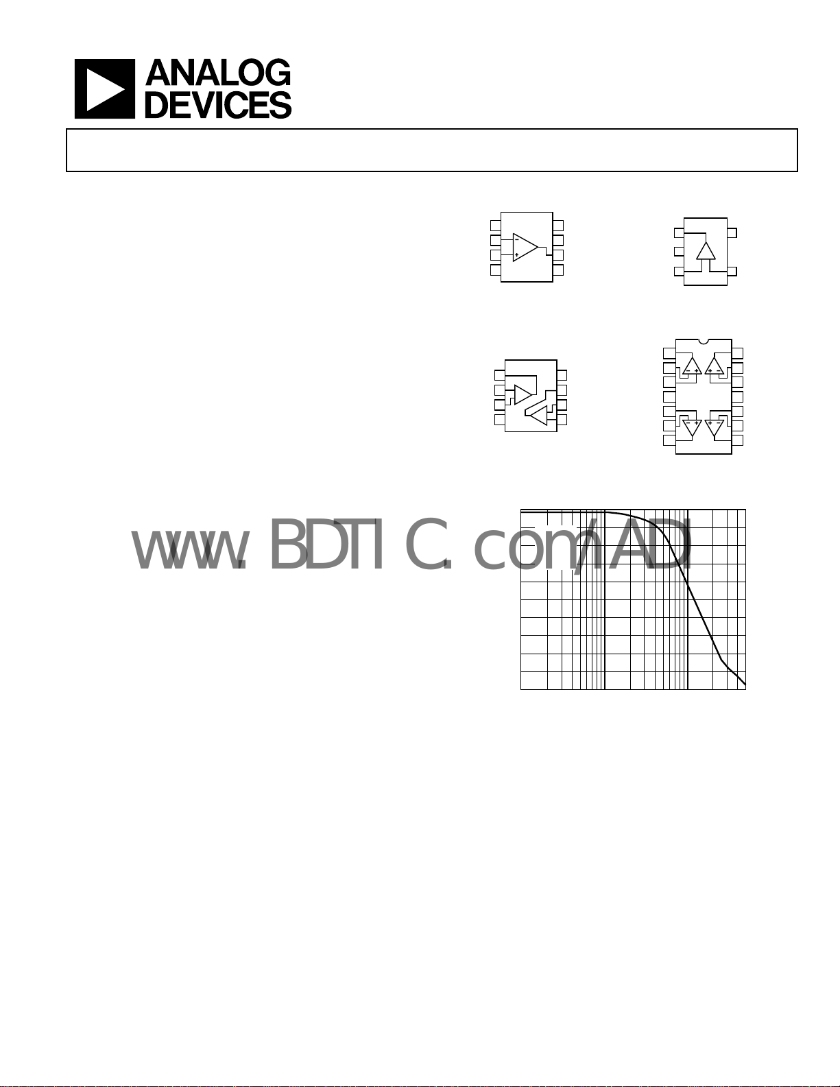
PIN CONNECTIONS (TOP VIEWS)
AD8051
1
NC
2
–IN
3
+IN
–V
4
S
NC = NO CONNECT
Figure 1. SOIC-8 (R) Figure 2
AD8052
1
OUT1
2
–IN1
3
+IN1
–V
4
S
Fig ure 3 . SOIC (R-8) and MSOP (RM-8) Figure 4. SOIC (R-14) and TSSOP (RU-14)
5.0
4.5
4.0
3.5
3.0
2.5
2.0
(THD ≤ 0.5%) (V)
1.5
1.0
0.5
PEAK-TO -PEAK OUT PUT VO LTAGE SWIN
0
8
NC
7
+V
S
6
V
OUT
5
NC
01062-001
OUT
–V
S
AD8051
1
2
3
+–
. SOT-23-5 (RJ)
1
OUT A
2
+V
8
–
+
= 5V
V
S
G = –1
R
= 2kΩ
F
= 2kΩ
R
L
S
OUT
7
6
–IN2
+IN2
5
01062-003
FREQUENCY (MHz)
–
+
0.1 1 10
–IN A
+IN A
+IN B
–IN B
OUT B
3
4
V+
AD8054
5
6
7
Figure 5. Low Distortion Rail-to-Rail Output Swing
5
+V
S
–IN+IN
4
01062-002
14
OUT D
13
–IN D
+IN D
12
11
V–
10
+IN C
–IN C
9
8
OUT C
50
1062-005
1062-004
GENERAL DESCRIPTION
The AD8051 (single), AD8052 (dual), and AD8054 (quad) are
low cost, high speed, voltage feedback amplifiers. The amplifiers
operate on +3 V, +5 V, or ±5 V supplies at low supply current.
They have true single-supply capability with an input voltage
range extending 200 mV below the negative rail and within 1 V
of the positive rail.
Despite their low cost, the AD8051/AD8052/AD8054 provide
exce
llent overall performance and versatility. The output voltage
swings to within 25 mV of each rail, providing maximum output
dynamic range with excellent overdrive recovery.
Rev. H
Information furnished by Analog Devices is believed to be accurate and reliable. However, no
responsibility is assumed by Anal og Devices for its use, nor for any infringements of patents or ot her
rights of third parties that may result from its use. Specifications subject to change without notice. No
license is granted by implication or otherwise under any patent or patent rights of Analog Devices.
Trademarks and registered trademarks are the property of their respective owners.
The AD8051/AD8052/AD8054 are well suited for video
lectronics, cameras, video switchers, or any high speed portable
e
equipment. Low distortion and fast settling make them ideal for
active filter applications.
The AD8051/AD8052 in the 8-lead SOIC, the AD8052 in the
MSO
P, the AD8054 in the 14-lead SOIC, and the 14-lead TSSOP
packages are available in the extended temperature range of
−40°C to +125°C.
One Technology Way, P.O. Box 9106, Norwood, MA 02062-9106, U.S.A.
Tel: 781.329.4700 www.analog.com
Fax: 781.461.3113 ©2007 Analog Devices, Inc. All rights reserved.
Page 2

AD8051/AD8052/AD8054
www.BDTIC.com/ADI
TABLE OF CONTENTS
Features .............................................................................................. 1
Applications....................................................................................... 1
Pin Connections (Top Views)......................................................... 1
General Description......................................................................... 1
Revision History ............................................................................... 2
Specifications..................................................................................... 3
Absolute Maximum Ratings............................................................ 9
Thermal Resistance ...................................................................... 9
Maximum Power Dissipation ..................................................... 9
ESD Caution.................................................................................. 9
Typical Performance Characteristics ........................................... 10
Theory of Operation ...................................................................... 16
REVISION HISTORY
12/07—Rev. G to Rev. H
Changes to Applications .................................................................. 1
Updated Outline Dimensions....................................................... 21
Changes to Ordering Guide.......................................................... 23
5/06—Rev. F to Rev. G
U
pdated Format.................................................................. Universal
Changes to Features, Applications, and General Description.....1
Changes to Figure 15...................................................................... 12
Changes to the Ordering Guide.................................................... 22
9/04—Rev. E to Rev. F
C
hanges to Ordering Guide.............................................................7
Changes to Figure 15...................................................................... 15
3/04—Rev. D to Rev. E
C
hanges to General Description .....................................................2
Changes to Specifications.................................................................3
Changes to Ordering Guide.............................................................6
Circuit Description .................................................................... 16
Application Information................................................................ 17
Overdrive Recovery ................................................................... 17
Driving Capacitive Loads.......................................................... 17
Layout Considerations............................................................... 18
Active Filters ............................................................................... 18
Analog-to-Digital and Digital-to-Analog Applications........ 19
Sync Stripper ............................................................................... 20
Single-Supply Composite Video Line Driver ......................... 20
Outline Dimensions ....................................................................... 21
Ordering Guide .......................................................................... 23
2/03—Rev. C to Rev. D
hanges to General Description .....................................................1
C
Changes to Specifications.................................................................3
Changes to Absolute Maximum Ratings........................................6
1/03—Rev. B to Rev. C
C
hanges to General Description .....................................................1
Changes to Pin Connections............................................................1
Changes to Specifications.................................................................2
Changes to Absolute Maximum Ratings........................................9
Changes to Figure 2...........................................................................9
Changes to Ordering Guide.............................................................9
Updated Outline Dimensions........................................................20
Rev. H | Page 2 of 24
Page 3

AD8051/AD8052/AD8054
www.BDTIC.com/ADI
SPECIFICATIONS
@ TA = 25°C, VS = 5 V, RL = 2 k to 2.5 V, unless otherwise noted.
Table 1.
AD8051A/AD8052A AD8054A
Parameter Conditions Min Typ Max Min Typ Max Unit
DYNAMIC PERFORMANCE
−3 dB Small Signal Bandwidth G = +1, V
G = −1, +2, V
Bandwidth for 0.1 dB Flatness
G = +2, V
= 150 Ω to 2.5 V
R
L
= 806 Ω (AD8051A/
R
F
AD8052A)
R
= 200 Ω (AD8054A) 12 MHz
F
Slew Rate G = −1, V
Full Power Response G = +1, V
Settling Time to 0.1% G = −1, V
NOISE/DISTORTION PERFORMANCE
Total Harmonic Distortion
1
fC = 5 MHz, V
G = +2
Input Voltage Noise f = 10 kHz 16 16 nV/√Hz
Input Current Noise f = 10 kHz 850 850 fA/√Hz
Differential Gain Error (NTSC) G = +2, RL = 150 Ω to 2.5 V 0.09 0.07 %
R
= 1 kΩ to 2.5 V 0.03 0.02 %
L
Differential Phase Error (NTSC) G = +2, RL = 150 Ω to 2.5 V 0.19 0.26 Degrees
R
= 1 kΩ to 2.5 V 0.03 0.05 Degrees
L
Crosstalk f = 5 MHz, G = +2 −60 −60 dB
DC PERFORMANCE
Input Offset Voltage 1.7 10 1.7 12 mV
T
MIN
Offset Drift 10 15 μV/°C
Input Bias Current 1.4 2.5 2 4.5 μA
T
MIN
Input Offset Current 0.1 0.75 0.2 1.2 μA
Open-Loop Gain RL = 2 kΩ to 2.5 V 86 98 82 98 dB
T
R
T
MIN
= 150 Ω to 2.5 V 76 82 74 82 dB
L
MIN
INPUT CHARACTERISTICS
Input Resistance 290 300 kΩ
Input Capacitance 1.4 1.5 pF
Input Common-Mode Voltage Range
Common-Mode Rejection Ratio VCM = 0 V to 3.5 V 72 88 70 86 dB
= 0.2 V p-p 70 110 80 150 MHz
OUT
= 0.2 V p-p 50 60 MHz
OUT
= 0.2 V p-p,
OUT
20 MHz
= 2 V step 100 145 140 170 V/μs
OUT
= 2 V p-p 35 45 MHz
OUT
= 2 V step 50 40 MHz
OUT
−67 −68 dB
25 30 mV
3.25 4.5 μA
96 96 dB
78 78 dB
−0.2 to
+4
−0.2 to
+4
− T
− T
− T
− T
MAX
MAX
MAX
MAX
= 2 V p-p,
OUT
V
Rev. H | Page 3 of 24
Page 4

AD8051/AD8052/AD8054
www.BDTIC.com/ADI
AD8051A/AD8052A AD8054A
Parameter Conditions Min Typ Max Min Typ Max Unit
OUTPUT CHARACTERISTICS
Output Voltage Swing RL = 10 kΩ to 2.5 V
R
R
Output Current V
T
Short-Circuit Current Sourcing 80 45 mA
Sinking 130 85 mA
Capacitive Load Drive G = +1 (AD8051/AD8052) 50 pF
G = +2 (AD8054) 40 pF
POWER SUPPLY
Operating Range 3 12 3 12 V
Quiescent Current/Amplifier 4.4 5 2.75 3.275 mA
Power Supply Rejection Ratio ΔVS = ±1 V 70 80 68 80 dB
OPERATING TEMPERATURE RANGE RJ-5 −40 +85 °C
RM-8, R-8, RU-14, R-14 −40 +125 −40 +125 °C
1
Refer to Figure 19.
= 2 kΩ to 2.5 V
L
= 150 Ω to 2.5 V
L
= 0.5 V to 4.5 V 45 30 mA
OUT
− T
MIN
MAX
0.1 to
4.9
0.3 to
4.625
45 30 mA
0.015 to
4.985
0.025 to
4.975
0.2 to
4.8
0.125 to
4.875
0.55 to
4.4
0.03 to
4.975
0.05 to
4.95
0.25 to
4.65
V
V
V
Rev. H | Page 4 of 24
Page 5

AD8051/AD8052/AD8054
www.BDTIC.com/ADI
@ TA = 25°C, VS = 3 V, RL = 2 k to 1.5 V, unless otherwise noted.
Table 2.
AD8051A/AD8052A AD8054A
Parameter Conditions Min Typ Max Min Typ Max Unit
DYNAMIC PERFORMANCE
−3 dB Small Signal Bandwidth G = +1, V
G = −1, +2, V
0.2 V p-p
Bandwidth for 0.1 dB Flatness
G = +2, V
= 150 Ω to 2.5 V
R
L
= 402 Ω (AD8051A/
R
F
AD8052A)
R
= 200 Ω (AD8054A) 10 MHz
F
Slew Rate G = −1, V
Full Power Response G = +1, V
Settling Time to 0.1% G = −1, V
NOISE/DISTORTION PERFORMANCE
Total Harmonic Distortion
1
fC = 5 MHz, V
G = −1, R
Input Voltage Noise f = 10 kHz 16 16 nV/√Hz
Input Current Noise f = 10 kHz 600 600 fA/√Hz
Differential Gain Error (NTSC) G = +2, VCM = 1 V
R
R
= 150 Ω to 1.5 V 0.11 0.13 %
L
= 1 kΩ to 1.5 V 0.09 0.09 %
L
Differential Phase Error (NTSC) G = +2, VCM = 1 V
R
R
= 150 Ω to 1.5 V 0.24 0.3 Degrees
L
= 1 kΩ to 1.5 V 0.10 0.1 Degrees
L
Crosstalk f = 5 MHz, G = +2 −60 −60 dB
DC PERFORMANCE
Input Offset Voltage 1.6 10 1.6 12 mV
T
MIN
Offset Drift 10 15 μV/°C
Input Bias Current 1.3 2.6 2 4.5 μA
T
MIN
Input Offset Current 0.15 0.8 0.2 1.2 μA
Open-Loop Gain RL = 2 kΩ 80 96 80 96 dB
T
R
T
MIN
= 150 Ω 74 82 72 80 dB
L
MIN
INPUT CHARACTERISTICS
Input Resistance 290 300 kΩ
Input Capacitance 1.4 1.5 pF
Input Common-Mode Voltage Range
Common-Mode Rejection Ratio VCM = 0 V to 1.5 V 72 88 70 86 dB
= 0.2 V p-p 70 110 80 135 MHz
OUT
=
OUT
= 0.2 V p-p,
OUT
50 65 MHz
17 MHz
= 2 V step 90 135 110 150 V/μs
OUT
= 1 V p-p 65 85 MHz
OUT
= 2 V step 55 55 ns
OUT
−47 −48 dB
25 30 mV
3.25 4.5 μA
94 94 dB
76 76 dB
−0.2 to
+2
−0.2 to
+2
= 100 Ω to 1.5 V
L
− T
MAX
− T
MAX
− T
MAX
− T
MAX
= 2 V p-p,
OUT
V
Rev. H | Page 5 of 24
Page 6

AD8051/AD8052/AD8054
www.BDTIC.com/ADI
AD8051A/AD8052A AD8054A
Parameter Conditions Min Typ Max Min Typ Max Unit
OUTPUT CHARACTERISTICS
Output Voltage Swing RL = 10 kΩ to 1.5 V
R
R
Output Current V
T
Short-Circuit Current Sourcing 60 30 mA
Sinking 90 50 mA
Capacitive Load Drive G = +1 (AD8051/AD8052) 45 pF
G = +2 (AD8054) 35 pF
POWER SUPPLY
Operating Range 3 12 3 12 V
Quiescent Current/Amplifier 4.2 4.8 2.625 3.125 mA
Power Supply Rejection Ratio ΔVS = 0.5 V 68 80 68 80 dB
OPERATING TEMPERATURE RANGE RJ-5 −40 +85 °C
RM-8, R-8, RU-14, R-14 −40 +125 −40 +125 °C
1
Refer to Figure 19.
= 2 kΩ to 1.5 V
L
= 150 Ω to 1.5 V
L
= 0.5 V to 2.5 V 45 25 mA
OUT
− T
MIN
MAX
0.0.75 to
2.9
0.2 to
2.75
45 25 mA
0.01 to
2.99
0.02 to
2.98
0.125 to
2.875
0.1 to
2.9
0.35 to
2.55
0.025 to
2.98
0.35 to
2.965
0.15 to
2.75
V
V
V
Rev. H | Page 6 of 24
Page 7

AD8051/AD8052/AD8054
www.BDTIC.com/ADI
@ TA = 25°C, VS = ±5 V, RL = 2 k to ground, unless otherwise noted.
Table 3.
AD8051A/AD8052A AD8054A
Parameter Conditions Min Typ Max Min Typ Max Unit
DYNAMIC PERFORMANCE
−3 dB Small Signal Bandwidth G = +1, V
G = −1, +2, V
Bandwidth for 0.1 dB Flatness
G = +2, V
= 150 Ω,
R
L
= 1.1 kΩ (AD8051A/
R
F
AD8052A)
R
= 200 Ω (AD8054A) 15 MHz
F
Slew Rate G = −1, V
Full Power Response G = +1, V
Settling Time to 0.1% G = −1, V
NOISE/DISTORTION PERFORMANCE
Total Harmonic Distortion
= 5 MHz, V
f
C
G = +2
Input Voltage Noise f = 10 kHz 16 16 nV/√Hz
Input Current Noise f = 10 kHz 900 900 fA/√Hz
Differential Gain Error (NTSC) G = +2, RL = 150 Ω 0.02 0.06 %
R
= 1 kΩ 0.02 0.02 %
L
Differential Phase Error (NTSC) G = +2, RL = 150 Ω 0.11 0.15 Degrees
R
= 1 kΩ 0.02 0.03 Degrees
L
Crosstalk f = 5 MHz, G = +2 −60 −60 dB
DC PERFORMANCE
Input Offset Voltage 1.8 11 1.8 13 mV
T
MIN
Offset Drift 10 15 μV/°C
Input Bias Current 1.4 2.6 2 4.5 μA
T
MIN
Input Offset Current 0.1 0.75 0.2 1.2 μA
Open-Loop Gain RL = 2 kΩ 88 96 84 96 dB
T
R
T
MIN
= 150 Ω 78 82 76 82 dB
L
MIN
INPUT CHARACTERISTICS
Input Resistance 290 300 kΩ
Input Capacitance 1.4 1.5 pF
Input Common-Mode Voltage Range
Common-Mode Rejection Ratio VCM = −5 V to +3.5 V 72 88 70 86 dB
OUTPUT CHARACTERISTICS
Output Voltage Swing RL = 10 kΩ
R
R
Output Current V
T
= 2 kΩ
L
= 150 Ω
L
OUT
MIN
Short-Circuit Current Sourcing 100 60 mA
Sinking 160 100 mA
Capacitive Load Drive G = +1 (AD8051/AD8052) 50 pF
G = +2 (AD8054) 40 pF
= 0.2 V p-p 70 110 85 160 MHz
OUT
= 0.2 V p-p 50 65 MHz
OUT
= 0.2 V p-p,
OUT
20 MHz
= 2 V step 105 170 150 190 V/μs
OUT
= 2 V p-p 40 50 MHz
OUT
= 2 V step 50 40 MHz
OUT
−71 −72 dB
27 32 mV
3.5 4.5 μA
96 96 dB
80 80 dB
−4.85 to
+4.85
−4.45 to
+4.3
−5.2 to
+4
−4.98 to
+4.98
−4.97 to
+4.97
−4.6 to
+4.6
−4.8 to
+4.8
−4.0 to
+3.8
−5.2 to
+4
−4.97 to
+4.97
−4.9 to
+4.9
−4.5 to
+4.5
V
V
V
V
− T
− T
− T
− T
MAX
MAX
MAX
MAX
= 2 V p-p,
OUT
= −4.5 V to +4.5 V 45 30 mA
− T
MAX
Rev. H | Page 7 of 24
45 30 mA
Page 8

AD8051/AD8052/AD8054
www.BDTIC.com/ADI
AD8051A/AD8052A AD8054A
Parameter Conditions Min Typ Max Min Typ Max Unit
POWER SUPPLY
Operating Range 3 12 3 12 V
Quiescent Current/Amplifier 4.8 5.5 2.875 3.4 mA
Power Supply Rejection Ratio ΔVS = ±1 68 80 68 80 dB
OPERATING TEMPERATURE RANGE RJ-5 −40 +85 °C
RM-8, R-8, RU-14, R-14 −40 +125 −40 +125 °C
Rev. H | Page 8 of 24
Page 9

AD8051/AD8052/AD8054
www.BDTIC.com/ADI
ABSOLUTE MAXIMUM RATINGS
Table 4.
Parameter Ratings
Supply Voltage 12.6 V
Internal Power Dissipation
SOIC Packages
SOT-23 Package
MSOP Package
TSSOP Package
Input Voltage (Common Mode) ±V
1
Observe power
ating curves
der
Observe power
ating curves
der
Observe power
ating curves
der
Observe power
ating curves
der
S
Differential Input Voltage ±2.5 V
Output Short-Circuit Duration
Observe power
ating curves
der
Storage Temperature Range (R) −65°C to +150°C
Operating Temperature Range (A Grade) −40°C to +125°C
Lead Temperature (Soldering 10 sec) 300°C
1
See Table 5.
Stresses above those listed under Absolute Maximum Ratings
may cause permanent damage to the device. This is a stress
rating only; functional operation of the device at these or any
other conditions above those indicated in the operational
section of this specification is not implied. Exposure to absolute
maximum rating conditions for extended periods may affect
device reliability.
THERMAL RESISTANCE
Specification is for device in free air.
Table 5. Thermal Resistance
Package Type θ
JA
8-Lead SOIC 125 °C/W
5-Lead SOT-23 180 °C/W
8-Lead MSOP 150 °C/W
14-Lead SOIC 90 °C/W
14-Lead TSSOP 120 °C/W
Unit
MAXIMUM POWER DISSIPATION
The maximum power that can be safely dissipated by the
AD8051/AD8052/AD8054 is limited by the associated rise in
junction temperature. The maximum safe junction temperature
for plastic encapsulated devices is determined by the glass
transition temperature of the plastic, approximately 150°C.
Temporarily exceeding this limit can cause a shift in parametric
performance due to a change in the stresses exerted on the die
by the package. Exceeding a junction temperature of 175°C for
an extended period can result in device failure.
While the AD8051/AD8052/AD8054 are internally shortc
ircuit protected, this cannot be sufficient to guarantee that the
maximum junction temperature (150°C) is not exceeded under
all conditions. To ensure proper operation, it is necessary to
observe the maximum power derating curves.
2.5
SOIC-14
SOIC-8
SOT-23-5
–35 –15 15 35 55 75 95 115
Figure 6. Maximum Power Dissipation vs.
Te
mperature for AD8051/AD8052/AD8054
5
AMBIENT TEMP ERATURE (°C)
01062-006
MAXIMUM POW ER DISSIPAT ION (W)
2.0
1.5
1.0
0.5
0
–55
TSSOP-14
MSOP-8
ESD CAUTION
Rev. H | Page 9 of 24
Page 10

AD8051/AD8052/AD8054
www.BDTIC.com/ADI
TYPICAL PERFORMANCE CHARACTERISTICS
3
2
1
0
–1
–2
–3
V
S
–4
GAIN AS SHOWN
NORMALIZ ED GAIN (dB)
R
F
–5
R
L
V
OUT
–6
–7
0.1 1 10 100
= 5V
AS SHOWN
= 2kΩ
= 0.2V p-p
G = +10
= 2kΩ
R
F
G = +2
R
= 2kΩ
F
G = +5
R
= 2kΩ
F
FREQUENCY (MHz )
G = +1
R
= 0
F
Figure 7. AD8051/AD8052 Normalized Gain vs. Frequency; V
500
= 5 V
S
01062-007
5
V
= 5V
S
4
GAIN AS SHOWN
3
R
R
2
V
1
0
–1
–2
–3
NORMALIZE D GAIN (dB)
–4
–5
–6
–7
100k
AS SHOWN
F
= 5kΩ
L
= 0.2V p-p
OUT
G = +10
= 2kΩ
R
F
1M
FREQUENCY (Hz)
G = +2
R
F
G = +5
= 2kΩ
R
F
10M 100M
= 2kΩ
Figure 10. AD8054 Normalized Gain vs. Frequency; V
G = +1
R
= 0
F
S
500M
= 5 V
01062-010
3
VSAS SHOWN
2
G=+1
=2kΩ
R
L
1
=0.2Vp-p
V
OUT
0
–1
–2
GAIN (dB)
–3
–4
–5
–6
–7
0.1 1 10 500
FREQUENCY (MHz)
VS = +3V
V
= ±5V
S
V
= +5V
S
100
Figure 8. AD8051/AD8052 Gain vs. Frequency vs. Supply
3
2
1
0
–1
–2
GAIN (dB)
–3
VS= 5V
–4
G=+1
=2kΩ
R
–5
L
=0.2Vp-p
V
OUT
TEMPERATURE AS SHOWN
–6
–7
0.1 500100
110
FREQUENCY (M Hz)
–40°C
+85°C
+25°C
Figure 9. AD8051/AD8052 Gain vs. Frequency vs. Temperature
6
G=+1
5
=2kΩ
R
L
= 5pF
C
L
4
=0.2Vp-p
V
OUT
3
2
1
GAIN (dB)
0
–1
–2
–3
–4
01062-008
100k
1M 10M 100M
FREQUE NCY (Hz)
+3V
+5V
+3V
+5V
±5V
±5V
500M
01062-011
Figure 11. AD8054 Gain vs. Frequency vs. Supply
4
= 5V
V
S
R
= 2kΩ TO 2.5V
3
L
C
= 5pF
L
2
G = +1
V
= 0.2V p-p
OUT
1
0
–1
GAIN (dB)
–2
–3
–4
–5
01062-009
101
FREQUE NCY (MHz )
–40°C
+85°C
+25°C
100
500
01062-012
Figure 12. AD8054 Gain vs. Frequency vs. Temperature
Rev. H | Page 10 of 24
Page 11

AD8051/AD8052/AD8054
www.BDTIC.com/ADI
6.3
6.2
6.1
6.0
5.9
5.8
5.7
VS = 5V
5.6
GAIN FLATNESS (dB)
G = +2
R
= 150Ω
L
5.5
R
= 806Ω
F
V
5.4
5.3
= 0.2V p- p
OUT
0.1 100
1 10
FREQUENCY (M Hz)
01062-013
Figure 13. AD8051/AD8052 0.1 dB Gain Flatness vs. Frequency; G = +2
6.3
6.2
6.1
6.0
5.9
5.8
5.7
VS = 5V
5.6
GAIN FLAT NESS (dB)
R
= 200Ω
F
R
= 150Ω
L
5.5
G = +2
5.4
V
= 0.2V p-p
OUT
5.3
1 10010
FREQUENCY (M Hz)
Figure 16. AD8054 0.1 dB Gain Flatness vs. Frequency; G = +2
01062-016
9
= ±5V
S
OUT
= 4V p-p
VS = +5V
V
= 2V p-p
OUT
01062-014
8
7
6
5
4
GAIN (dB)
3
AS SHOWN
V
S
2
G = +2
R
= 2kΩ
F
1
R
= 2kΩ
L
V
AS SHOWN
OUT
0
–1
0.1 1 10 100 500
V
V
FREQUENCY (MHz)
Figure 14. AD8051/AD8052 Large Signal Frequency Response; G = +2
80
= 5V
V
70
60
50
40
30
20
10
OPEN-LOOP GAIN (dB)
0
–10
–20
0.01 0.1 1 10 100 500
PHASE
GAIN
FREQUENCY (MHz)
S
R
= 2kΩ
L
50° PHASE
MARGIN
0
–45
–90
–135
–180
PHASE MARGIN (Degrees)
Figure 15. AD8051/AD8052 Open-Loop Gain and Phase vs. Frequency
9
8
7
6
5
4
GAIN (dB)
3
VS AS SHOWN
2
G = +2
R
= 2kΩ
F
1
R
= 2kΩ
L
V
AS SHOWN
OUT
0
–1
0.1 1 10 100 500
VS = ±5V
V
OUT
FREQUENCY (MHz)
= 4V p-p
VS = +5V
V
= 2V p-p
OUT
01062-017
Figure 17. AD8054 Large Signal Frequency Response; G = +2
80
V
= 5V
70
60
50
40
30
20
10
OPEN-LOOP GAIN (dB)
0
–10
–20
30k 100k 1M 10M 100M 500M
01062-015
Figure 18. AD8054 Open-Loop Gain a
GAIN
PHASE
FREQUENCY (Hz)
nd Phase Margin vs. Frequency
S
R
= 2kΩ
L
C
= 5pF
L
45° PHASE
MARGIN
180
135
90
45
0
PHASE MARGIN (Degrees)
01062-018
Rev. H | Page 11 of 24
Page 12

AD8051/AD8052/AD8054
–
–
√
www.BDTIC.com/ADI
20
V
= 2V p-p VS = 3V, G = –1
OUT
–30
–40
= 5V, G = +1
V
S
R
= 100Ω
L
12345678
FUNDAMENTAL F REQUENCY (MHz)
TOTAL HARMONIC DISTORTION (dBc)
–100
–110
–50
–60
–70
–80
–90
= 5V, G = +2
V
S
R
= 2kΩ, RL = 100Ω
F
V
= 5V, G = +2
S
R
= 2kΩ, RL = 2kΩ
F
R
= 2kΩ, RL = 100Ω
F
V
= 5V, G = +1
S
R
= 2kΩ
L
910
Figure 19. Total Harmonic Distortion
01062-019
1000
100
VOLTAGE NOISE (nA/√Hz)
= 5V
V
S
10
1
10
1k 10k 100k
FREQUENCY (Hz)
Figure 22. Input Voltage Noise vs. Frequency
1M
10M100
1062-022
30
–40
–50
–60
–70
–80
–90
–100
–110
WORST HARMO NIC (dBc)
–120
–130
–140
05.04.5
10MHz
5MHz
1MHz
0.5 1.0 1. 5 2.0 2. 5 3. 0 3.5 4.0
OUTPUT VOLTAGE (V p-p)
VS = 5V
R
= 2kΩ
L
G = +2
Figure 20. Worst Harmonic vs. Output Voltage
0.10
NTSC SUBSCRIBER (3. 58MHz)
0.08
0.06
0.04
0.02
0.00
–0.02
DIFFERENT IAL
DIFFERENTIAL
VS = 5V, G = +2
GAIN ERROR (%)
–0.04
R
= 2kΩ, RLAS SHOWN
F
–0.06
0 102030405060708090100
0.10
0.05
0.00
–0.05
–0.10
–0.15
VS = 5V, G = +2
–0.20
R
= 2kΩ, RLAS SHOWN
F
–0.25
PHASE ERROR (Deg rees)
0 102030405060708090100
MODULATING RAMP LEVEL (IRE)
R
= 1kΩ
L
R
L
R
R
= 150Ω
= 1kΩ
L
= 150Ω
L
Figure 21. AD8051/AD8052 Differential Gain and Phase Errors
100
VS = 5V
Hz)
10
1
CURRENT NOISE (p A/
0.1
10
01062-020
DIFFERENTIAL
DIFFERENT IAL
01062-021
Figure 23. Input Current Noise vs. Frequency
0.10
NTSC SUBSCRIBER (3.58MHz)
0.05
0.00
–0.05
VS = 5V, G = +2
GAIN ERROR (%)
R
= 2kΩ, RL AS SHOWN
F
–0.10
1ST2ND3RD4TH5TH6TH7TH8TH9TH10TH11
0.3
0.2
0.1
0.0
–0.1
VS = 5V, G = +2
–0.2
R
= 2kΩ, RL AS SHOWN
F
–0.3
PHASE ERROR (Degrees)
1ST2ND3RD4TH5TH6TH7TH8TH9TH10TH11
1k 10k 100k
FREQUENCY (Hz)
RL = 1kΩ
RL = 150Ω
RL = 1kΩ
MODULATING RAMP LEVEL (I RE)
1M
RL = 150Ω
10M100
01062-023
TH
TH
01062-024
Figure 24. AD8054 Differential Gain and Phase Errors
Rev. H | Page 12 of 24
Page 13

AD8051/AD8052/AD8054
–
–
www.BDTIC.com/ADI
10
VS = 5V
–20
R
= 2kΩ
F
R
= 2kΩ
L
–30
V
= 2V p-p
OUT
–40
–50
–60
–70
CROSSTALK (dB)
–80
–90
–100
0.1 500100
Figure 25. AD8052 Crosstalk (Output-t
110
FREQUE NCY (MHz)
o-Output) vs. Frequency
01062-025
10
VS = ±5V
–20
R
= 1kΩ
F
R
=AS SHOWN
L
–30
V
= 2V p-p
OUT
–40
–50
–60
–70
CROSSTALK (d B)
–80
–90
–100
–110
0.1 1 10 100 500
Figure 28. AD8054 Crosstalk (Output-t
RL = 100Ω
= 1kΩ
R
L
FREQUENCY (M Hz)
o-Output) vs. Frequency
01062-028
0
VS = 5V
–10
–20
–30
–40
–50
CMRR (dB)
–60
–70
–80
–90
–100
0.03 0. 1 1 10 100 500
FREQUENCY (MHz)
Figure 26. CMRR vs. Frequency
100.000
OUTPUT RESI STANCE (Ω)
VS=5V
G = +1
31.000
10.000
3.100
1.000
0.310
0.100
0.031
0.010
0.1 1 10 100 500
Figure 27. Closed-Loop Output R
FREQUENCY (MHz)
esistance vs. Frequency
20
VS = 5V
10
0
–10
–20
–30
PSRR (d B)
–40
–50
–60
–70
–80
0.01 0.1 1 10 100 500
01062-026
–PSRR
+PSRR
FREQUENCY (MHz)
01062-029
Figure 29. PSRR vs. Frequency
70
= 5V
V
S
G = –1
60
R
= 2kΩ
L
50
40
30
20
SETTLING TIME TO 0.1% (ns)
10
0
01062-027
0.5 1.0 1.5 2. 0
AD8051/AD8052
AD8054
INPUT STEP (V p-p)
01062-030
Figure 30. Settling Time vs. Input Step
Rev. H | Page 13 of 24
Page 14

AD8051/AD8052/AD8054
www.BDTIC.com/ADI
1.0
VS = 5V
0.9
0.8
0.7
0.6
0.5
0.4
0.3
0.2
OUTPUT SAT URATION VO LTAGE ( V)
0.1
0
V
OH
LOAD CURRENT (mA)
V
= +25°C
V
OH
= –40°C
= +85°C
OH
V
OL
= –40°C
V
V
OL
= +85°C
OL
= +25°C
80 85757065605550454035302520151050
01062-031
Figure 31. AD8051/AD8052 Output Saturation Voltage vs. Load Current
100
RL = 2kΩ
90
1.000
OUTPUT SAT URATION VO LTAGE (V)
0.875
0.750
0.625
0.500
0.375
0.250
0.125
0
VS = 5V
+5V – V
(–40°C)
+5V – V
OH
V
(–40°C)
OL
LOAD CURRENT (mA)
+5V – V
OH
V
OL
(+125°C)
OH
(+25°C)
(+25°C)
V
OL
(+125°C)
Figure 33. AD8054 Output Saturation Voltage vs. Load Current
302724211815129630
01062-033
R
= 150Ω
L
80
OPEN-LOOP GAIN (dB)
70
VS = 5V
60
054.54.03. 53.02.52.01.51. 00.5
OUTPUT VOLTAGE (V)
Figure 32. Open-Loop Gain vs. Output Voltage
.0
01062-032
Rev. H | Page 14 of 24
Page 15

AD8051/AD8052/AD8054
www.BDTIC.com/ADI
2µs
= 2 kΩ
L
VS = 5V
G = –1
= 2kΩ
R
F
= 2kΩ
R
L
VS = 5V
G = +1
= 2kΩ
R
L
1062-037
VIN = 0.1V p- p
G = +1
= 2kΩ
R
L
= 3V
V
S
1.5
VOLTS
20mV
20ns
1062-034
Figure 34. 100 mV Step Response, G = +1
VS = 5V
G = +1
= 2kΩ
R
L
2.6
2.5
VOLTS
2.4
5.0
2.5
VOLTS
1V
Figure 37. Output Swing; G = −1, R
2.55
2.50
VOLTS
2.45
50mV
Figure 35. AD8051/AD8052 200 mV Step Response; V
4.5
3.5
2.5
VOLTS
1.5
0.5
VIN = 1V p-p
G = +2
= 2kΩ
R
L
= 5V
V
S
500mV
Figure 36. Large Signal Step Response; V
20ns
= 5 V, G = +1
S
20ns
= 5 V, G = +2
S
01062-035
Figure 38. AD8054 100 mV Step Response; V
4
3
2
1
VOLTS
–1
–2
–3
–4
1062-036
Figure 39. Large Signal Step Response; V
50mV 40ns
= 5 V, G = +1
S
1V
20ns
= ±5 V, G = +1
S
VS = ±5V
G = +1
R
= 2kΩ
L
01062-038
01062-039
Rev. H | Page 15 of 24
Page 16

AD8051/AD8052/AD8054
V
V
www.BDTIC.com/ADI
THEORY OF OPERATION
CIRCUIT DESCRIPTION
The AD8051/AD8052/AD8054 are fabricated on the Analog
Devices, Inc. proprietary eXtra-Fast Complementary Bipolar
(XFCB) process, which enables the construction of PNP and
NPN transistors with similar fTs in the 2 GHz to 4 GHz region.
The process is dielectrically isolated to eliminate the parasitic
and latch-up problems caused by junction isolation. These
features allow the construction of high frequency, low distortion
amplifiers with low supply currents. This design uses a differential
output input stage to maximize bandwidth and headroom (see
Figure 40). The smaller signal swings required on the first stage
utputs (nodes SIP, SIN) reduce the effect of nonlinear currents
o
due to junction capacitances and improve the distortion performance. This design achieves harmonic distortion of −80 dBc
@ 1 MHz into 100 with V
single 5 V supply.
= 2 V p-p (gain = +1) on a
OUT
CC
R26
Q4
R2
R15
VINP
IN
N
Q13
Q1
Q40
V
SIP
I10
R39
Q5
EE
SIN
I2 I3
The inputs of the device can handle voltages from −0.2 V below
e negative rail to within 1 V of the positive rail. Exceeding
th
these values do not cause phase reversal; however, the input
ESD devices begin to conduct if the input voltages exceed the
rails by greater than 0.5 V. During this overdrive condition, the
output stays at the rail.
The rail-to-rail output range of the AD8051/AD8052/AD8054
is p
rovided by a complementary common emitter output stage.
High output drive capability is provided by injecting all output
stage predriver currents directly into the bases of the output
devices Q8 and Q36. Biasing of Q8 and Q36 is accomplished by
I8 and I5, along with a common-mode feedback loop (not
shown). This circuit topology allows the AD8051/AD8052 to
drive 45 mA of output current and allows the AD8054 to drive
30 mA of output current with the outputs within 0.5 V of the
supply rails.
Q22
Q25
Q7
Q39
Q51
R27
R23
Q21 Q27
Q50
Q31
Q23
I9
Q36
I5
V
EE
C3
V
OUT
C9
Q2
C7
V
EE
R5
Q3
R21
Q11
R3
Q24 Q47
I7
I11
Q8
I8
V
CC
01062-045
Figure 40. AD8051/AD8052 Simplified Schematic
Rev. H | Page 16 of 24
Page 17

AD8051/AD8052/AD8054
www.BDTIC.com/ADI
APPLICATION INFORMATION
OVERDRIVE RECOVERY
Overdrive of an amplifier occurs when the output and/or input
range is exceeded. The amplifier must recover from this overdrive condition. As shown in Figure 41, the AD8051/AD8052/
AD8054 r
within 45 ns from positive overdrive.
ecover within 60 ns from negative overdrive and
VS = ±5V
INPUT 1V/DIV
OUTPUT 2V/DIV
VOLTS
V/DIV AS SHOWN
Figure 41. Overdrive Recovery
G = +5
R
R
100ns
= 2kΩ
F
= 2kΩ
L
01062-040
2.60
2.55
2.50
VOLTS
2.45
2.40
50mV
Figure 43. AD8051/AD8052 200 mV Step Response; C
10000
VS = 5V
≤ 30%
OVERSHOOT
1000
RS = 3Ω
RS = 0Ω
VS = 5V
G = +1
R
C
100ns
= 2kΩ
L
= 50pF
L
= 50 pF
L
1062-042
DRIVING CAPACITIVE LOADS
Consider the AD8051/AD8052 in a closed-loop gain of +1 with
= 5 V and a load of 2 k in parallel with 50 pF. Figure 42
+V
S
and Figure 43 show their frequency and time domain responses,
r
espectively, to a small-signal excitation. The capacitive load
drive of the AD8051/AD8052/AD8054 can be increased by
adding a low value resistor in series with the load.
nd Figure 45 show the effect of a series resistor on the capaci-
a
t
ive drive for varying voltage gains. As the closed-loop gain is
increased, the larger phase margin allows for larger capacitive
loads with less peaking. Adding a series resistor with lower
closed-loop gains accomplishes the same effect. For large
capacitive loads, the frequency response of the amplifier is
dominated by the roll-off of the series resistor and the load
capacitance.
8
6
4
2
0
–2
GAIN (dB)
–4
VS = 5V
–6
G = +1
= 2kΩ
R
L
–8
= 50pF
C
L
= 200mV p-p
V
OUT
–10
–12
0.1 500100
Figure 42. AD8051/AD8052 Closed-Loop Frequency Response; C
110
FREQUENCY (M Hz)
Figure 44
= 50 pF
L
01062-041
100
R
R
F
G
CAPACITIVE LOAD (pF)
10
1
1234 56
V
100mV
STEP
IN
50Ω
ACL (V/V)
R
S
V
OUT
C
L
Figure 44. AD8051/AD8052 Capacitive Load Drive vs. Closed-Loop Gain
1000
VS = 5V
≤ 30%
OVERSHOOT
RS = 10Ω
R
= 0Ω
S
100
R
R
F
G
CAPACITIVE L OAD (pF)
10
1234 56
V
100mV
STEP
IN
50Ω
ACL (V/V)
Figure 45. AD8054 Capacitive Load Drive vs. Closed-Loop Gain
R
S
V
OUT
C
L
01062-043
01062-044
Rev. H | Page 17 of 24
Page 18

AD8051/AD8052/AD8054
V
www.BDTIC.com/ADI
LAYOUT CONSIDERATIONS
The specified high speed performance of the AD8051/AD8052/
AD8054 requires careful attention to board layout and component
selection. Proper RF design techniques and low parasitic
component selection are necessary.
The PCB should have a ground plane covering all unused
p
ortions of the component side of the board to provide a low
impedance path. The ground plane should be removed from the
area near the input pins to reduce parasitic capacitance.
Chip capacitors should be used for supply bypassing. One end
sh
ould be connected to the ground plane and the other within
3 mm of each power pin. An additional large (4.7 µF to 10 µF)
tantalum electrolytic capacitor should be connected in parallel,
but not necessarily so close, to supply current for fast, large
signal changes at the output.
The feedback resistor should be located close to the inverting
input pin to keep the parasitic capacitance at this node to a
minimum. Parasitic capacitance of less than 1 pF at the inverting
input can significantly affect high speed performance.
Stripline design techniques should be used for long signal traces
(g
reater than about 25 mm). These should be designed with a
characteristic impedance of 50 or 75 and be properly
terminated at each end.
ACTIVE FILTERS
Active filters at higher frequencies require wider bandwidth op
amps to work effectively. Excessive phase shift produced by
lower frequency op amps can significantly affect active filter
performance.
Figure 46 shows an example of a 2 MHz biquad bandwidth filter
tha
t uses three op amps of an AD8054. Such circuits are
sometimes used in medical ultrasound systems to lower the
noise bandwidth of the analog signal before analog-to-digital
conversion.
Note that the unused amplifier’s inputs should be tied to ground.
R6
1kΩ
C1
50pF
8
13
14
12
BAND-PASS
FILTER OUTPUT
8054
R2
2kΩ
R1
3kΩ
2
IN
1
3
AD8054
Figure 46. 2 MHz Biquad Band-Pass Filter Using AD
R3
2kΩ
R4
2kΩ
6
5
AD8054
2kΩ
7
C2
50pF
R5
9
10
AD8054
The frequency response of the circuit is shown in Figure 47.
0
–10
–20
GAIN (dB)
–30
–40
10k 100k 1M 10M 100M
Figure 47. Frequency Response of 2 MHz Band-Pass Biquad Filter
FREQUENCY (Hz)
01062-047
01062-046
Rev. H | Page 18 of 24
Page 19

AD8051/AD8052/AD8054
www.BDTIC.com/ADI
ANALOG-TO-DIGITAL AND DIGITAL-TO-ANALOG APPLICATIONS
Figure 50 is a schematic showing the AD8051 used as a driver
for an AD9201, a 10-bit, 20 MSPS, dual analog-to-digital
onverter. This converter is designed to convert I and Q signals in
c
communications systems. In this application, only the I channel
is being driven. The I channel is enabled by applying a logic
high to SELECT (Pin 13).
The AD8051 is running from a dual supply and is configured
r a gain of +2. The input signal is terminated in 50 and the
fo
output is 2 V p-p, which is the maximum input range of the
AD9201. The 22 series resistor limits the maximum current
th
at flows and helps to lower the distortion of the ADC.
The AD9201 has differential inputs for each channel. These are
desig
nated the A and B inputs. The B inputs of each channel are
connected to VREF (Pin 22), which supplies a positive reference
of 2.5 V. Each of the B inputs has a small low-pass filter that also
helps to reduce distortion.
The output of the op amp is ac-coupled into INA-I (Pin 16) via
wo parallel capacitors to provide good high frequency and low
t
frequency coupling. The 1 k resistor references the signal to
VREF that is applied to INB-I. Thus, INA-I swings both positive
and negative with respect to the bias voltage applied to INB-I.
With the sampling clock running at 20 MSPS, the analog-to-
ital output was analyzed with a digital analyzer. Two input
dig
frequencies were used, 1 MHz and 9.5 MHz, which is just short
of the Nyquist frequency. These signals were well filtered to
minimize any harmonics.
Figure 48 shows the FFT response of the ADC for the case of a
1 MH
z analog input. The SFDR is 71.66 dB, and the analog-todigital is producing 8.8 ENOB (effective number of bits). When
the analog frequency was raised to 9.5 MHz, the SFDR was
reduced to −60.18 dB and the ADC operated with 8.46 ENOBs
wn in Figure 49. The inclusion of the AD8051 in the
as sho
c
ircuit did not worsen the distortion performance of the AD9201.
10
FUND
0
–10
–20
–30
–40
–50
–60
–70
AMPLITUDE (dB)
–80
–90
–100
–110
–120
012345678910
2ND
4TH3RD
5TH
6TH
FREQUENCY (MHz)
7TH
8TH
9TH
PART# 0
FFTSIZE 8192
20.0MHz
FCLK
998.5kHz
FUND
–0.51dB
VIN
–68.13
THD
SNR
54.97
54.76
SINAD
8.80
ENOB
SFDR
71.66
2ND
–74.53
3RD
–76.06
4TH
–76.35
5TH
–79.05
6TH
–80.36
7TH
–75.08
8TH
–88.12
9TH
–77.87
Figure 48. FFT Plot for AD8051 Driving the AD9201 at 1 MHz
10
0
–10
–20
–30
–40
–50
2ND
–60
–70
AMPLIT UDE (dB)
–80
–90
–100
–110
–120
0 123 4567 8 910
4TH
8TH
6TH
FREQUEN CY (MHz)
7TH
3RD
5TH
Figure 49. FFT Plot for AD8051 Driving the AD9201 at 9.5 MHz
FUND
PART#
FFTSIZE 8192
FCLK
20.0MHz
FUND
9.5MHz
VIN
–0.44dB
THD
–57.08
SNR
54.65
SINAD
52.69
ENOB
8.46
60.18
SFDR
–60.18
2ND
–60.23
3RD
–82.01
4TH
–78.83
5TH
6TH
–81.28
–77.28
7TH
–84.54
8TH
–92.78
9TH
0
01062-049
01062-050
15
10pF
SLEEP
16
INA-I
INB -I
17
REFT-I
18
19
REFB- I
AVSS
20
21
REFSENSE
VREF
22
23
AVDD
REFB -Q
24
REFT -Q
25
INB-Q
26
INA-Q
27
CHIP–SELECT
28
AD9201
50Ω
3
AD8051
2
+5V
–5V
0.33µF
1kΩ
10µF0.1µF
7
6
4
10µF0.1µF
0.01µF
22Ω
1kΩ
+5V
1kΩ
10µF
22Ω
22Ω
10µF0.1µF 0.1µF
0.1µF
10µF
10µF0.1µF 0.1µF
0.1µF
22Ω
10pF
10pF
0.1µF
0.1µF
22Ω
10pF
Figure 50. The AD8051 Driving an AD9201, a 10-Bit, 20 MSPS Analog-to-Digital Converter
Rev. H | Page 19 of 24
CLOCK
SELECT
DVDD
DVSS
14
13
12
D9
11
D8
D7
10
D6
9
D5
8
D4
7
D3
6
5
D2
4
D1
3
D0
2
1
+V
DD
DATA OUT
0.1µF 10µF
+5V
01062-048
Page 20

AD8051/AD8052/AD8054
V
V
www.BDTIC.com/ADI
SYNC STRIPPER
Synchronizing pulses are sometimes carried on video signals so
as not to require a separate channel to carry the synchronizing
information. However, for some functions, such as analog-todigital conversion, it is not desirable to have the sync pulses on
the video signal. These pulses reduce the dynamic range of the
video signal and do not provide any useful information for such
a function.
A sync stripper removes the synchronizing pulses from a video
sig
nal while passing all the useful video information. Figure 51
sho
ws a practical single-supply circuit that uses only a single
AD8051. It is capable of directly driving a reverse terminated
o line.
vide
IDEO WITHOUT SYNC
+
0.1µF
6
R2
1kΩ
GROUND
10µF
TO A/D
100Ω
V
BLANK
GROUND
IDEO WITH SYNC
V
IN
(OR 2 × V
0.4V
3V OR 5V
7
3
AD8051
2
4
R1
1kΩ
0.8V
)
BLANK
Figure 51. Sync Stripper
The video signal plus sync is applied to the noninverting input
with the proper termination. The amplifier gain is set to 2 via
the two 1 kΩ resistors in the feedback circuit. A bias voltage
must be applied to R1 so that the input signal has the sync
pulses stripped at the proper level.
The blanking level of the input video pulse is the desired place to
emove the sync information. This level is multiplied by 2 by the
r
amplifier. This level must be at ground at the output for the sync
stripping action to take place. Since the gain of the amplifier from
the input of R1 to the output is −1, a voltage equal to 2 × V
BLANK
must be applied to make the blanking level come out at ground.
SINGLE-SUPPLY COMPOSITE VIDEO LINE DRIVER
Many composite video signals have their blanking level at
ground and have video information that is both positive and
negative. Such signals require dual-supply amplifiers to pass
them. However, by ac level shifting, a single-supply amplifier
can be used to pass these signals. The following complications
can arise from such techniques.
Signals of bounded peak-to-peak amplitude that vary in duty
c
ycle require larger dynamic swing capacity than their (bounded)
peak-to-peak amplitude after they are ac-coupled. As a worst
case, the dynamic signal swing will approach twice the peak-topeak value. The two conditions that define the maximum
Rev. H | Page 20 of 24
1062-051
dynamic swing requirements are a signal that is mostly low but
goes high with a duty cycle that is a small fraction of a percent,
and the other extreme defined by the opposite condition.
The worst case of composite video is not quite this demanding.
e bounding condition is a signal that is mostly black for an
On
entire frame but has a white (full amplitude) minimum width
spike at least once in a frame.
The other extreme is for a full white video signal. The blanking
tervals and sync tips of such a signal have negative-going
in
excursions in compliance with the composite video specifications.
The combination of horizontal and vertical blanking intervals
limit such a signal to being at the highest (white) level for a
maximum of about 75% of the time.
As a result of the duty cycles between the two extremes
p
reviously presented, a 1 V p-p composite video signal that is
multiplied by a gain of 2 requires about 3.2 V p-p of dynamic
voltage swing at the output for an op amp to pass a composite
video signal of arbitrarily varying duty cycle without distortion.
Some circuits use a sync tip clamp to hold the sync tips at a
elatively constant level to lower the amount of dynamic signal
r
swing required. However, these circuits can have artifacts, such
as sync tip compression, unless they are driven by a source with
a very low output impedance. The AD8051/AD8052/AD8054
have adequate signal swing when running on a single 5 V
supply to handle an ac-coupled composite video signal.
The input to the circuit in
(1 V p-p) vide
o signal that has the blanking level at ground. The
Figure 52 is a standard composite
input network level shifts the video signal by means of ac coupling.
The noninverting input of the op amp is biased to half of the
supply voltage.
The feedback circuit provides unity gain for the dc-biasing of
t
he input and provides a gain of 2 for any signals that are in the
video bandwidth. The output is ac-coupled and terminated to
drive the line.
The capacitor values were selected for providing minimum tilt
or
field time distortion of the video signal. These values would
be required for video that is considered to be studio or broadcast
quality. However, if a lower consumer grade of video, sometimes
referred to as consumer video, is all that is desired, the values
and the cost of the capacitors can be reduced by as much as a
factor of five with minimum visible degradation in the picture.
5V
4.99kΩ
+
COMPOSI TE
VIDEO
IN
75Ω
4.99kΩ
47µF
R
T
Figure 52. Single-Supply Composite Video Line Driver
10µF
3
AD8051
2
220µF
7
4
+
10kΩ
R
G
1kΩ
R
1kΩ
0.1µF
6
F
1000µF
+
0.1µF
+
10µF
R
75Ω
BT
V
OUT
R
L
75Ω
1062-052
Page 21

AD8051/AD8052/AD8054
www.BDTIC.com/ADI
OUTLINE DIMENSIONS
8.75 (0.3445)
8.55 (0.3366)
BSC
8
7
6.20 (0.2441)
5.80 (0.2283)
1.75 (0.0689)
1.35 (0.0531)
SEATING
PLANE
8°
0°
0.25 (0.0098)
0.17 (0.0067)
0.50 (0.0197)
0.25 (0.0098)
1.27 (0.0500)
0.40 (0.0157)
45°
060606-A
4.00 (0.1575)
3.80 (0.1496)
0.25 (0.0098)
0.10 (0.0039)
COPLANARIT Y
0.10
14
1
1.27 (0.0500)
0.51 (0.0201)
0.31 (0.0122)
CONTROLL ING DIMENSIONS ARE IN MILLI METERS; INCH DIMENSIONS
(IN PARENTHESES) ARE ROUNDED-O FF MIL LIMETER EQUIVALENTS FOR
REFERENCE ON LY AND ARE NOT APPROPRI ATE FOR USE IN DESIGN.
COMPLIANT TO JEDEC STANDARDS MS-012-AB
Figure 53. 14-Lead Standard Small Outline Package [SOIC_N]
Narrow B
ody (R-14)
Dimensions shown in millimeters and (inches)
2.90 BSC
1.60 BSC
1.30
1.15
0.90
0.15 MAX
5
123
PIN 1
COMPLIANT TO JEDEC STANDARDS MO-178-A A
1.90
BSC
0.50
0.30
4
2.80 BSC
0.95 BSC
1.45 MAX
SEATING
PLANE
0.22
0.08
10°
5°
0°
0.60
0.45
0.30
Figure 54. 5-Lead Small Outline Transistor Package [SOT-23]
(RJ-5)
ensions shown in millimeters
Dim
Rev. H | Page 21 of 24
Page 22

AD8051/AD8052/AD8054
www.BDTIC.com/ADI
0.95
0.85
0.75
0.15
0.00
COPLANARITY
3.20
3.00
2.80
8
5
4
SEATING
PLANE
5.15
4.90
4.65
1.10 MAX
0.23
0.08
3.20
3.00
1
2.80
PIN 1
0.65 BSC
0.38
0.22
0.10
COMPLIANT TO JEDEC STANDARDS MO-187-AA
8°
0°
0.80
0.60
0.40
Figure 55. 8-Lead Mini Small Outline Package [MSOP]
(RM-8)
Dim
ensions shown in millimeters
5.00 (0.1968)
4.80 (0.1890)
4.00 (0.1574)
3.80 (0.1497)
85
1
6.20 (0.2441)
5.80 (0.2284)
4
1.27 (0.0500)
BSC
0.25 (0.0098)
0.10 (0.0040)
COPLANARITY
0.10
SEATING
PLANE
CONTROLL ING DIMENSI ONS ARE IN MILLIM ETERS; INCH DI MENSIONS
(IN PARENTHESES) ARE ROUNDED-OFF MILLIMETER EQUIVALENTS FOR
REFERENCE ONLY AND ARE NOT APPROPRI ATE FOR USE IN DES IGN.
COMPLIANT TO JEDEC STANDARDS MS-012-A A
1.75 (0.0688)
1.35 (0.0532)
0.51 (0.0201)
0.31 (0.0122)
8°
0°
0.25 (0.0098)
0.17 (0.0067)
0.50 (0.0196)
0.25 (0.0099)
1.27 (0.0500)
0.40 (0.0157)
45°
012407-A
Figure 56. 8-Lead Standard Small Outline Package [SOIC_N]
Narrow B
ody (R-8)
Dimensions shown in millimeters and (inches)
5.10
5.00
4.90
14
4.50
4.40
4.30
PIN 1
1.05
1.00
0.80
0.65
BSC
0.15
0.05
COMPLIANT TO JEDEC STANDARDS MO-153-AB-1
Figure 57. 14-Lead Thin Shrink S
8
6.40
BSC
71
0.20
1.20
0.09
MAX
0.30
SEATING
0.19
PLANE
COPLANARITY
0.10
mall Outline Package [TSSOP]
(RU-14)
Dimensions shown in millimeters
8°
0°
0.75
0.60
0.45
Rev. H | Page 22 of 24
Page 23

AD8051/AD8052/AD8054
www.BDTIC.com/ADI
ORDERING GUIDE
Model Temperature Range Package Description Package Option Branding
AD8051AR −40°C to +125°C 8-Lead SOIC_N R-8
AD8051AR-REEL −40°C to +125°C 8-Lead SOIC_N, 13" Tape and Reel R-8
AD8051AR-REEL7 −40°C to +125°C 8-Lead SOIC_N, 7" Tape and Reel R-8
AD8051ARZ1 −40°C to +85°C 8-Lead SOIC_N R-8
AD8051ARZ-REEL1 −40°C to +85°C 8-Lead SOIC_N, 13" Tape and Reel R-8
AD8051ARZ-REEL71 −40°C to +85°C 8-Lead SOIC_N, 7" Tape and Reel R-8
AD8051ART-R2 −40°C to +85°C 5-Lead SOT-23, 7" Tape and Reel RJ-5 H2A
AD8051ART-REEL −40°C to +85°C 5-Lead SOT-23, 13" Tape and Reel RJ-5 H2A
AD8051ART-REEL7 −40°C to +85°C 5-Lead SOT-23, 7" Tape and Reel RJ-5 H2A
AD8051ARTZ-R21 −40°C to +85°C 5-Lead SOT-23, 7" Tape and Reel RJ-5 H06
AD8051ARTZ-REEL1 −40°C to +85°C 5-Lead SOT-23, 13" Tape and Reel RJ-5 H06
AD8051ARTZ-REEL71 −40°C to +85°C 5-Lead SOT-23, 7" Tape and Reel RJ-5 H06
AD8052AR −40°C to +125°C 8-Lead SOIC_N R-8
AD8052AR-REEL −40°C to +125°C 8-Lead SOIC_N, 13" Tape and Reel R-8
AD8052AR-REEL7 −40°C to +125°C 8-Lead SOIC_N, 7" Tape and Reel R-8
AD8052ARZ1 −40°C to +125°C 8-Lead SOIC_N R-8
AD8052ARZ-REEL1 −40°C to +125°C 8-Lead SOIC_N, 13" Tape and Reel R-8
AD8052ARZ-REEL71 −40°C to +125°C 8-Lead SOIC_N, 7" Tape and Reel R-8
AD8052ARM −40°C to +125°C 8-Lead MSOP RM-8 H4A
AD8052ARM-REEL −40°C to +125°C 8-Lead MSOP, 13" Tape and Reel RM-8 H4A
AD8052ARM-REEL7 −40°C to +125°C 8-Lead MSOP, 7" Tape and Reel RM-8 H4A
AD8052ARMZ
AD8052ARMZ-REEL71 −40°C to +125°C 8-Lead MSOP, 7" Tape and Reel RM-8 H4A#
AD8054AR −40°C to +125°C 14-Lead SOIC_N R-14
AD8054AR-REEL −40°C to +125°C 14-Lead SOIC_N, 13" Tape and Reel R-14
AD8054AR-REEL7 −40°C to +125°C 14-Lead SOIC_N, 7" Tape and Reel R-14
AD8054ARZ1 −40°C to +125°C 14-Lead SOIC_N R-14
AD8054ARZ-REEL1 −40°C to +125°C 14-Lead SOIC_N, 13" Tape and Reel R-14
AD8054ARZ-REEL71 −40°C to +125°C 14-Lead SOIC_N, 7" Tape and Reel R-14
AD8054ARU −40°C to +125°C 14-Lead TSSOP RU-14
AD8054ARU-REEL −40°C to +125°C 14-Lead TSSOP, 13" Tape and Reel RU-14
AD8054ARU-REEL7 −40°C to +125°C 14-Lead TSSOP, 7" Tape and Reel RU-14
AD8054ARUZ1 −40°C to +125°C 14-Lead TSSOP RU-14
AD8054ARUZ-REEL1 −40°C to +125°C 14-Lead TSSOP, 13" Tape and Reel RU-14
AD8054ARUZ-REEL71 −40°C to +125°C 14-Lead TSSOP, 7" Tape and Reel RU-14
1
Z = RoHS Compliant Part. # denotes lead-free product may be top or bottom marked.
1
−40°C to +125°C 8-Lead MSOP RM-8 H4A#
Rev. H | Page 23 of 24
Page 24

AD8051/AD8052/AD8054
www.BDTIC.com/ADI
NOTES
©2007 Analog Devices, Inc. All rights reserved. Trademarks and
registered trademarks are the property of their respective owners.
D01062-0-12/07(H)
Rev. H | Page 24 of 24
 Loading...