

Page 1
160 MHz Rail-to-Rail
FREQUENCY – MHz
VS = +5V
G = +2
R
F
= 400Ω
0
100
NORMALIZED GAIN – dB
80
60
40
20
0
+2
+1
–2
–1
–8
–7
–6
–5
–4
–3
a
FEATURES
Fully Specified for +3 V, +5 V, and 65 V Supplies
Output Swings Rail to Rail
Input Voltage Range Extends 200 mV Below Ground
No Phase Reversal with Inputs 1 V Beyond Supplies
Disable/Power-Down Capability
Low Power of 5.2 mA (26 mW on +5 V)
High Speed and Fast Settling on +5 V:
160 MHz –3 dB Bandwidth (G = +1)
160 V/ms Slew Rate
30 ns Settling Time to 0.1%
Good Video Specifications (R
Gain Flatness of 0.1 dB to 30 MHz
0.03% Differential Gain Error
0.038 Differential Phase Error
Low Distortion
–69 dBc Worst Harmonic @ 10 MHz
Outstanding Load Drive Capability
Drives 50 mA 0.5 V from Supply Rails
Cap Load Drive of 45 pF
APPLICATIONS
Power Sensitive High Speed Systems
Video Switchers
Distribution Amplifiers
A/D Driver
Professional Cameras
CCD Imaging Systems
Ultrasound Equipment (Multichannel)
Single-Supply Multiplexer
PRODUCT DESCRIPTION
The AD8041 is a low power voltage feedback, high speed amplifier designed to operate on +3 V, +5 V or ± 5 V supplies. It
has true single supply capability with an input voltage range
extending 200 mV below the negative rail and within 1 V of the
positive rail.
= 150 V, G = +2)
L
Amplifier with Disable
AD8041
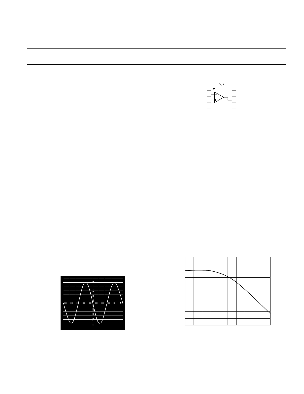
CONNECTION DIAGRAM
8-Pin Plastic Mini-DIP and SOIC
NC
1
–INPUT
2
+INPUT
3
AD8041
–V
4
S
(Top View)
NC = NO CONNECT
The output voltage swing extends to within 50 mV of each rail,
providing the maximum output dynamic range. Additionally, it
features gain flatness of 0.1 dB to 30 MHz while offering differential gain and phase error of 0.03% and 0.03° on a single +5 V
supply. This makes the AD8041 ideal for professional video
electronics such as cameras, video switchers or any high speed
portable equipment. The AD8041’s low distortion and fast settling make it ideal for buffering high speed A-to-D converters.
The AD8041 has a high speed disable feature useful for multiplexing or for reducing power consumption (1.5 mA). The disable logic interface is compatible with CMOS or open-collector
logic. The AD8041 offers low power supply current of 5.8 mA
max and can run on a single +3 V power supply. These features
are ideally suited for portable and battery powered applications
where size and power are critical.
The wide bandwidth of 160 MHz along with 160 V/µs of slew
rate on a single +5 V supply make the AD8041 useful in many
general purpose high speed applications where dual power supplies of up to ±6 V and single supplies from +3 V to +12 V are
needed. The AD8041 is available in 8-pin plastic DIP and
SOIC over the industrial temperature range of –40°C to +85°C.
8
DISABLE
7
+V
OUTPUT
6
NC
5
S
REV. 0
Information furnished by Analog Devices is believed to be accurate and
reliable. However, no responsibility is assumed by Analog Devices for its
use, nor for any infringements of patents or other rights of third parties
which may result from its use. No license is granted by implication or
otherwise under any patent or patent rights of Analog Devices.
5V
2.5V
0V
1V
200ns
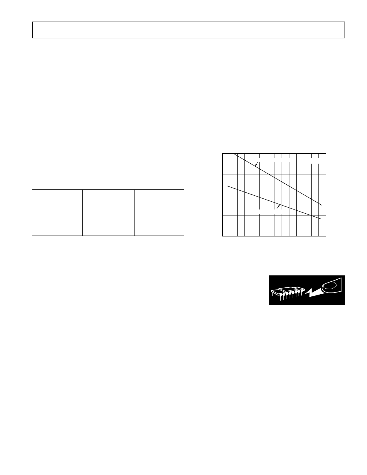
Figure 1. Output Swing: Gain = –1, VS = +5 V
Figure 2. Frequency Response: Gain = +2, VS = +5 V
© Analog Devices, Inc., 1995
One Technology Way, P.O. Box 9106, Norwood. MA 02062-9106, U.S.A.
Tel: 617/329-4700 Fax: 617/326-8703
Page 2

AD8041–SPECIFICATIONS
(@ TA = +258C, VS = +5 V, RL = 2 kΩ to 2.5 V, unless otherwise noted)
AD8041A
Parameter Conditions Min Typ Max Units
DYNAMIC PERFORMANCE
–3 dB Small Signal Bandwidth, V
Bandwidth for 0.1 dB Flatness G = +2, R
Slew Rate G = –1, V
Full Power Response V
Settling Time to 0.1% G = –1, V
< 0.5 V p-p G = +1 130 160 MHz
O
= 2 V p-p 24 MHz
O
= 150 Ω 30 MHz
L
= 2 V Step 130 160 V/µs
O
= 2 V Step 35 ns
O
Settling Time to 0.01% 55 ns
NOISE/DISTORTION PERFORMANCE
Total Harmonic Distortion f
Input Voltage Noise f = 10 kHz 16 nV/√
Input Current Noise f = 10 kHz 600 fA/√
Differential Gain Error (NTSC) G = +2, R
Differential Phase Error (NTSC) G = +2, R
= 5 MHz, VO = 2 V p-p, G = +2, RL = 1 kΩ –72 dB
C
= 150 Ω to 2.5 V 0.03 %
L
= 150 Ω to 2.5 V 0.03 Degrees
L
G = +2, R
= 75 Ω to 2.5 V 0.01 %
L
Hz
Hz
G = +2, RL = 75 Ω to 2.5 V 0.19 Degrees
DC PERFORMANCE
Input Offset Voltage 27mV
T
MIN–TMAX
8mV
Offset Drift 10 µV/°C
Input Bias Current 1.2 2 µA
T
MIN–TMAX
3 µA
Input Offset Current 0.2 0.5 µA
Open-Loop Gain R
= 1 kΩ 86 95 dB
L
T
MIN–TMAX
90 dB
INPUT CHARACTERISTICS
Input Resistance 160 kΩ
Input Capacitance 1.8 pF
Input Common-Mode Voltage Range –0.2 to 4 V
Common-Mode Rejection Ratio VCM = 0 V to 3.5 V 74 80 dB
OUTPUT CHARACTERISTICS
Output Voltage Swing: R
Output Voltage Swing: R
Output Voltage Swing: R
Output Current V
= 10 kΩ 0.05 to 4.95 V
L
= 1 kΩ 0.35 to 4.75 0.1 to 4.9 V
L
= 50 Ω 0.4 to 4.4 0.3 to 4.5 V
L
= 0.5 V to 4.5 V 50 mA
OUT
Short Circuit Current Sourcing 90 mA
Sinking 150 mA
Capacitive Load Drive G = +1 45 pF
POWER SUPPLY
Operating Range 312V
Quiescent Current 5.2 5.8 mA
Quiescent Current (Disabled) 1.4 1.7 mA
Power Supply Rejection Ratio VS = 0, +5 V, ±1 V 72 80 dB
DISABLE CHARACTERISTICS V
Turn-Off Time R
Turn-On Time R
Off Isolation (Pin 8 Tied to –V
)R
S
Off Voltage (Device Disabled) <+V
On Voltage (Device Enabled) Open or +V
Specifications subject to change without notice.
= 2 V p-p @ 10 MHz, G = + 2
O
= RL = 2 kΩ 120 ns
F
= RL = 2 kΩ 230 ns
F
= 100 Ω, f = 5 MHz, G = +2, RF = 1 kΩ 70 dB
L
– 0.25 V
S
S
V
–2–
REV. 0
Page 3

AD8041
SPECIFICATIONS
Parameter Conditions Min Typ Max Units
DYNAMIC PERFORMANCE
–3 dB Small Signal Bandwidth, V
Bandwidth for 0.1 dB Flatness G = +2, R
Slew Rate G = –1, V
Full Power Response V
Settling Time to 0.1% G = –1, V
Settling Time to 0.01% 55 ns
NOISE/DISTORTION PERFORMANCE
Total Harmonic Distortion f
Input Voltage Noise f = 10 kHz 16 nV/√
Input Current Noise f = 10 kHz 600 fA/√
Differential Gain Error (NTSC) G = +2, R
Differential Phase Error (NTSC) G = +2, RL = 150 Ω to 1.5 V, Input VCM = 1 V 0.05 Degrees
DC PERFORMANCE
Input Offset Voltage 27mV
Offset Drift 10 µV/°C
Input Bias Current 1.2 2.3 µA
Input Offset Current 0.2 0.6 µA
Open-Loop Gain R
INPUT CHARACTERISTICS
Input Resistance 160 kΩ
Input Capacitance 1.8 pF
Input Common-Mode Voltage Range –0.2 to 2 V
Common-Mode Rejection Ratio VCM = 0 V to 1.5 V 72 80 dB
(@ TA = +258C, VS = +3 V, RL = 2 kΩ to 1.5 V, unless otherwise noted)
AD8041A
< 0.5 V p-p G = +1 120 150 MHz
O
= 2 V p-p 20 MHz
O
= 5 MHz, VO = 2 V p-p, G = –1, RL = 100 Ω –55 dB
C
T
MIN–TMAX
T
MIN–TMAX
= 1 kΩ 85 94 dB
L
T
MIN–TMAX
= 150 Ω 25 MHz
L
= 2 V Step 120 150 V/µs
O
= 2 V Step 40 ns
O
= 150 Ω to 1.5 V, Input VCM = 1 V 0.07 %
L
8mV
3 µA
89 dB
Hz
Hz
OUTPUT CHARACTERISTICS
Output Voltage Swing: R
Output Voltage Swing: R
Output Voltage Swing: R
Output Current V
= 10 kΩ 0.05 to 2.95 V
L
= 1 kΩ 0.45 to 2.7 0.1 to 2.9 V
L
= 50 Ω 0.5 to 2.6 0.25 to 2.75 V
L
= 0.5 V to 2.5 V 50 mA
OUT
Short Circuit Current Sourcing 70 mA
Sinking 120 mA
Capacitive Load Drive G = +1 40 pF
POWER SUPPLY
Operating Range 312V
Quiescent Current 5.0 5.6 mA
Quiescent Current (Disabled) 1.3 1.5 mA
Power Supply Rejection Ratio VS = 0, +3 V, ±0.5 V 68 80 dB
DISABLE CHARACTERISTICS V
Turn-Off Time R
Turn-On Time R
Off Isolation (Pin 8 Tied to –V
)R
S
Off Voltage (Device Disabled) <+V
On Voltage (Device Enabled) Open or +V
Specifications subject to change without notice.
= 2 V p-p @ 10 MHz, G = +2
O
= RL = 2 kΩ 90 ns
F
= RL = 2 kΩ 170 ns
F
= 100 Ω, f = 5 MHz, G = +2, RF = 1 kΩ 70 dB
L
– 0.25 V
S
S
V
REV. 0
–3–
Page 4

AD8041–SPECIFICATIONS
(@ TA = +258C, VS = 65 V, RL = 2 kΩ to 0 V, unless otherwise noted)
AD8041A
Parameter Conditions Min Typ Max Units
DYNAMIC PERFORMANCE
–3 dB Small Signal Bandwidth, V
Bandwidth for 0.1 dB Flatness G = +2, R
Slew Rate G = –1, V
Full Power Response V
Settling Time to 0.1% G = –1, V
< 0.5 V p-p G = +1 140 170 MHz
O
= 2 V p-p 26 MHz
O
= 150 Ω 32 MHz
L
= 2 V Step 140 170 V/µs
O
= 2 V Step 30 ns
O
Settling Time to 0.01% 50 ns
NOISE/DISTORTION PERFORMANCE
Total Harmonic Distortion f
Input Voltage Noise f = 10 kHz 16 nV/√
Input Current Noise f = 10 kHz 600 fA/√
Differential Gain Error (NTSC) G = +2, R
Differential Phase Error (NTSC) G = +2, R
= 5 MHz, VO = 2 V p-p, G = +2, RL = 1 kΩ –77 dB
C
= 150 Ω 0.02 %
L
= 150 Ω 0.03 Degrees
L
G = +2, R
= 75 Ω 0.02 %
L
Hz
Hz
G = +2, RL = 75 Ω 0.10 Degrees
DC PERFORMANCE
Input Offset Voltage 27mV
T
MIN–TMAX
8mV
Offset Drift 10 µV/°C
Input Bias Current 1.2 2.3 µA
T
MIN–TMAX
3 µA
Input Offset Current 0.2 0.6 µA
Open-Loop Gain R
= 1 kΩ 90 99 dB
L
T
MIN–TMAX
95 dB
INPUT CHARACTERISTICS
Input Resistance 160 kΩ
Input Capacitance 1.8 pF
Input Common-Mode Voltage Range –5.2 to 4 V
Common-Mode Rejection Ratio VCM = –5 V to 3.5 V 72 80 dB
OUTPUT CHARACTERISTICS
Output Voltage Swing: R
Output Voltage Swing: R
Output Voltage Swing: R
Output Current V
= 10 kΩ –4.95 to +4.95 V
L
= 1 kΩ –4.45 to +4.6 –4.8 to +4.8 V
L
= 50 Ω –4.3 to +3.2 –4.5 to +3.8 V
L
= –4.5 V to 4.5 V 50 mA
OUT
Short Circuit Current Sourcing 100 mA
Sinking 160 mA
Capacitive Load Drive G = +1 50 pF
POWER SUPPLY
Operating Range 312V
Quiescent Current 5.8 6.5 mA
Quiescent Current (Disabled) 1.6 2.2 mA
Power Supply Rejection Ratio VS = –5, +5 V, ±1 V 68 80 dB
DISABLE CHARACTERISTICS V
Turn-Off Time R
Turn-On Time R
Off Isolation (Pin 8 Tied to –V
)R
S
Off Voltage (Device Disabled) <+V
On Voltage (Device Enabled) Open or +V
Specifications subject to change without notice.
= 2 V p-p @ 10 MHz, G = +2
O
= 2 kΩ 120 ns
F
= 2 kΩ 320 ns
F
= 100 Ω, f = 5 MHz, G = +2, RF = 1 kΩ 70 dB
L
– 0.25 V
S
S
–4–
REV. 0
Page 5
AD8041
WARNING!
ESD SENSITIVE DEVICE
ABSOLUTE MAXIMUM RATINGS
Supply Voltage . . . . . . . . . . . . . . . . . . . . . . . . . . . . . . . +12.6 V
Internal Power Dissipation
2
1
Plastic Package (N) . . . . . . . . . . . . . . . . . . . . . . . 1.3 Watts
Small Outline Package (R) . . . . . . . . . . . . . . . . . . 0.9 Watts
Input Voltage (Common Mode) . . . . . . . . . . . . . . . . . . . . ±V
S
Differential Input Voltage . . . . . . . . . . . . . . . . . . . . . . ±3.4 V
Output Short Circuit Duration
. . . . . . . . . . . . . . . . . . . . . . Observe Power Derating Curves
Storage Temperature Range N, R . . . . . . . . –65°C to +125°C
Operating Temperature Range (A Grade) . . . –40°C to +85°C
Lead Temperature Range (Soldering 10 sec) . . . . . . . . +300°C
NOTES
1
Stresses above those listed under “Absolute Maximum Ratings” may cause
permanent damage to the device. This is a stress rating only and functional
operation of the device at these or any other conditions above those indicated in the
operational section of this specification is not implied. Exposure to absolute
maximum rating conditions for extended periods may affect device reliability.
2
Specification is for the device in free air:
8-Pin Plastic Package: θJA = 90°C/Watt
8-Pin SOIC Package: θJA = 160°C/Watt.
ORDERING GUIDE
Temperature Package
Model Range Option
AD8041AN –40°C to +85°C 8-Pin Plastic DIP
AD8041AR –40°C to +85°C 8-Pin Plastic SOIC
AD8041AR-REEL REEL-SOIC
AD8041-EB Evaluation Board
MAXIMUM POWER DISSIPATION
The maximum power that can be safely dissipated by the
AD8041 is limited by the associated rise in junction temperature. The maximum safe junction temperature for plastic encapsulated devices is determined by the glass transition temperature
of the plastic, approximately +150°C. Exceeding this limit temporarily may cause a shift in parametric performance due to a
change in the stresses exerted on the die by the package. Exceeding a junction temperature of +175°C for an extended period can result in device failure.
While the AD8041 is internally short circuit protected, this may
not be sufficient to guarantee that the maximum junction temperature (+150°C) is not exceeded under all conditions. To ensure proper operation, it is necessary to observe the maximum
power derating curves.
2.0
8-PIN MINI-DIP PACKAGE
1.5
1.0
0.5
MAXIMUM POWER DISSIPATION – Watts
0
–50 90–40 –30 –20 –10 0 10 20 30 50 60 70 8040
8-PIN SOIC PACKAGE
AMBIENT TEMPERATURE – °C
TJ = +150°C
Figure 3. Maximum Power Dissipation vs. Temperature
CAUTION
ESD (electrostatic discharge) sensitive device. Electrostatic charges as high as 4000 V readily
accumulate on the human body and test equipment and can discharge without detection.
Although the AD8041 features proprietary ESD protection circuitry, permanent damage may
occur on devices subjected to high energy electrostatic discharges. Therefore, proper ESD
precautions are recommended to avoid performance degradation or loss of functionality.
REV. 0
–5–
Page 6

LOAD RESISTANCE – Ω
100
70
95
90
85
80
75
0 2000250 500 750 1000 1250 1500 1750
VS = +5V
T = +25°C
OPEN-LOOP GAIN – dB
TEMPERATURE – °C
100
97
85
–60 –40 –20 0 20 40 60 80 100 120
94
91
88
OPEN-LOOP GAIN – dB
VS = +5V
R
L
= 1kΩ TO +2.5V
OUTPUT VOLTAGE – Volts
100
70
40
90
80
60
50
050.5 1 1.5 2 2.5 3 3.5 4 4.5
RL = 500Ω TO +2.5V
VS = +5V
RL = 50Ω TO +2.5V
OPEN-LOOP GAIN – dB
AD8041–Typical Performance Characteristics
30
VS = ±2.5V
T = +25°C
25
91 PARTS
MEAN = +0.21
STD DEVIATION = 1.47
20
15
10
NUMBER OF PARTS IN BIN
5
0
–6 6–5 –4 –3 –2 –1 0 1 2 3 4 5
V
– mV
OS
Figure 4. Typical Distribution of V
0.20
MEAN = 0.02µV/°C
STD DEV = 2.87µV/°C
0.15
0.10
PROBABILITY DENSITY
0.05
0
–10 10–7.5
–5 –2.5 0 2.5 5 7.5
VOS DRIFT – µV/°C
SAMPLE SIZE = 45
Figure 5. VOS Drift Over –40°C to +85°C
2
VS = +5V
V
CM
1.5
= 0V
OS
Figure 7. Open-Loop Gain vs. RL to +25°C
Figure 8. Open-Loop Gain vs. Temperature
1
0.5
INPUT BIAS CURRENT – µA
0
–45 85–35
–25 –15 –5 5 15 25 35 45 55 65 75
Figure 6. IB vs. Temperature
TEMPERATURE – °C
–6–
Figure 9. Open-Loop Gain vs. Output Voltage
REV. 0
Page 7

AD8041
FREQUENCY – MHz
6.5
6.4
5.5
6.3
6.2
6.1
6.0
5.9
5.8
5.7
5.6
1 50010
CLOSED-LOOP GAIN – dB
100
32.4MHz
VS= +5V
G = +2
R
L
= 150Ω TO 2.5V
R
F
= 402Ω
200
150
100
50
INPUT VOLTAAGE NOISE – nV/ √Hz
REV. 0
0
10 100k100
1k 10k
FREQUENCY – Hz
Figure 10. Input Voltage Noise vs. Frequency
–30
–40
–50
–60
VS = +5V, AV = +1,
= 100Ω TO 2.5V
R
L
–70
–80
–90
TOTAL HARMONIC DISTORTION – dBc
–100
1102
FUNDAMENTAL FREQUENCY – MHz
VS = +5V, AV = +2,
R
L
VS = +5V, AV = +1,
= 1kΩ TO 2.5V
R
L
VS = +3V, AV = –1,
R
= 100Ω TO 1.5V
L
= 100Ω TO 2.5V
VS = +5V, AV = +2,
= 1kΩ TO 2.5V
R
L
3456789
Figure 11. Total Harmonic Distortion
–30
–40
–50
–60
–70
–80
–90
–100
–110
WORST HARMONIC – dBc
–120
–130
–140
0 1.50.5 1 2
Figure 12. Worst Harmonic vs. Output Voltage
OUTPUT VOLTAGE – V
2.5
10MHz
5MHz
1MHz
VS = +5V
= 2kΩ TO +2.5V
R
L
GAIN = +2
3 3.5 4 4.5 5
PP
–7–
Figure 13. Differential Gain and Phase Errors
Figure 14. 0.1 dB Gain Flatness
+120
+100
GAIN
+80
+60
+40
PHASE
+20
OPEN-LOOP GAIN – dB
0
–20
–40
0.0
0.1
FREQUENCY – MHz
VS = +5V
R
= 2kΩ TO +2.5V
L
C
= 5pF TO +2.5V
L
100101
Figure 15. Open-Loop Gain and Phase Margin
vs. Frequency
+180
+135
90
45
0
–45
–90
PHASE MARGIN – Degrees
–135
–180
500
Page 8

AD8041–Typical Performance Characteristics
5
VS= +5V
4
= 2kΩ TO 2.5V
R
L
= 5pF
C
3
L
G =+1
2
1
0
–1
–2
CLOSED-LOOP GAIN – dB
–3
–4
–5
1 50010 100
T = +125°C
T = +25°C
T = –55°C
FREQUENCY – MHz
Figure 16. Closed-Loop Frequency Response
vs. Temperature
5
GAIN = +1
4
R
= 2kΩ
L
CL= 5pF
3
2
1
0
–1
–2
CLOSED-LOOP GAIN – dB
–3
–4
–5
1 50010 100
VS = +3V
RL & CL TO 1.5V
VS = +5V
RL & CL TO 2.5V
FREQUENCY – MHz
VS = ±5V
50
G = –1
40
30
TIME – ns
20
10
0.5 21 1.5
VS = +3V, 0.1%
VS = ±5V, 0.1%
VS = +3V, 1%
VS = ±5V, 1%
INPUT STEP – Volts p-p
Figure 19. Settling Time vs. Input Step
–10
–20
VS = +3V AND ±5V
–30
–40
–50
–60
–70
CMRR – dB
–80
–90
–100
–110
0.01
1 50010 1000.1
FREQUENCY – MHz
Figure 17. Closed-Loop Frequency Response vs. Supply
100
GAIN = +1
V
= +5V
S
10
1
0.1
OUTPUT RESISTANCE – Ω
0.01
0.01
1 50010 1000.1
FREQUENCY – MHz
Figure 18. Output Resistance vs. Frequency
Figure 20. CMRR vs. Frequency
0.60
0.50
0.40
0.30
0.20
0.10
OUTPUT SATURATION VOLTAGE – Volts
VS = +5V
C
°
+125
OH,
+5V – V
+5V – V
, –55
V
OL
0
0505
10 15 20 25 30 35 40 45
LOAD CURRENT – mA
C
°
–55
OH,
C
°
, +125
V
OL
C
°
Figure 21. Output Saturation Voltage vs. Load Current
–8–
REV. 0
Page 9

AD8041
FREQUENCY – Hz
5
4
–5
NORMALIZED OUTPUT (DB)
3
2
1
0
–1
–2
–3
–4
1M 500M10M 100M
G = +2
G = +10
G = +5
G = +2,
R
L
= 402Ω
VS = +5V
R
L
= 5KΩ TO +2.5V
R
F
= 2kΩ
8
7
6
5
4
SUPPLY CURRENT – mA
3
2
–60 –40 –20 0 20 40 60 80 100 120
TEMPERATURE – °C
VS = ±5V
VS = +5V
VS = +3V
Figure 22. Supply Current vs. Temperature
40
20
VS = +5V
0
–20
–40
–60
PSRR – dB
–80
–100
–120
–140
–160
0.01
–PSRR
+PSRR
1 50010 1000.1
FREQUENCY – MHz
90
80
70
60
50
06010
20° PHASE
MARGIN
40
30
CAPACITIVE LOAD – pF
20
10
0
100kΩ
1kΩ
V
IN
20 30 40 50
SERIES RESISTANCE – Ω
R
SERIES
C
LOAD
VS = +5V
45° PHASE
MARGIN
Figure 25. Capacitive Load vs. Series Resistance
Figure 23. PSRR vs. Frequency
10
9
8
7
6
5
p-p – Volts
4
OUT
V
3
2
REV. 0
1
0
0.1 10001 10 100
Figure 24. Output Voltage Swing vs. Frequency
FREQUENCY – MHz
VS = ±5V
RL = 2kΩ
Figure 26. Frequency Response vs. Closed-Loop Gain
1.600V
1.575V
1.550V
1.525V
1.500V
1.475V
1.450V
1.425V
1.400V
50mV
V
I
N
R
L
VS = +3V
G = +1
Figure 27. Pulse Response, VS = +3 V
–9–
= 0.1V p-p
=
2kΩ
10ns
Page 10

AD8041–Typical Performance Characteristics
3V
2.5V
2V
1.5V
1V
0.5V
0V
2µs
500mV
VIN = 3V p-p
f = 0.1MHz
R
L
= 2kΩ
V
S
= +3V
G = –1
3V
2.5V
2V
1.5V
1V
0.5V
0V
2µs
500mV
VIN = 2.8V p-p
f = 0.8MHz
R
L
= 2kΩ
V
S
= +3V
G = –1
5V
4V
3V
2V
1V
0V
5V
4V
3V
1V
4.840V MAX
0.111V MIN
Figure 28a.
4.741V MAX
RL = 150Ω TO +2.5V
200µs
RL = 150Ω TO GND
2.6V
2.55V
2.5V
2.45V
2.4V
50mV
VS = +5V
G = +1
R
= 2kΩ
L
V
= 5pF
L
40ns
Figure 30. 100 mV Step Response, VS = +5 V, G = +1
2V
1V
0V
1V
0.043V MIN
Figure 28b.
200µs
Figure 31. Output Swing, VS = +3 V, VIN = 3 V p-p
Figure 28a-b. Output Swing vs. Load Reference Voltage,
= +5 V, G = –1
V
S
4.5V
VS = +5V
G = +2
R
= 2kΩ
3.5V
2.5V
1.5V
0.5V
Figure 29. One Volt Step Response, VS = +5 V, G = +2
V
L
= 1V p-p
IN
40ns1V
Figure 32. Output Swing, VS = +3 V, VIN = 2.8 V p-p
–10–
REV. 0
Page 11

AD8041
Overdrive Recovery
Overdrive of an amplifier occurs when the output and/or input
range are exceeded. The amplifier must recover from this overdrive condition. As shown in Figure 33, the AD8041 recovers
within 50 ns from negative overdrive and within 25 ns from
positive overdrive.
5V
OUTPUT
INPUT
2.5V
0V
G = +2
= +5V
V
S
40ns50mV
Figure 33. Overdrive Recovery
Circuit Description
The AD8041 is fabricated on Analog Devices’ proprietary
eXtra-Fast Complementary Bipolar (XFCB) process which enables the construction of PNP and NPN transistors with similar
f
s in the 2 GHz–4 GHz region. The process is dielectrically iso-
T
lated to eliminate the parasitic and latch-up problems caused by
junction isolation. These features allow the construction of high
frequency, low distortion amplifiers with low supply currents.
This design uses a differential output input stage to maximize
bandwidth and headroom (see Figure 34). The smaller signal
swings required on the first stage outputs (nodes S1P, S1N)
reduce the effect of nonlinear currents due to junction
capacitances and improve the distortion performance. With this
design harmonic distortion of better than –85 dB @ 1 MHz into
100 Ω with V
= 2 V p-p (Gain = +2) on a single 5 volt sup-
OUT
ply is achieved.
The complementary common-emitter design of the output stage
provides excellent load drive without the need for emitter followers, thereby improving the output range of the device considerably with respect to conventional op amps. High output drive
capability is provided by injecting all output stage predriver currents directly into the bases of the output devices Q8 and Q36.
Biasing of Q8 and Q36 is accomplished by I8 and I5, along with
a common-mode feedback loop (not shown). This circuit topology allows the AD8041 to drive 50 mA of output current with
the outputs within 0.5 V of the supply rails.
On the input side, the device can handle voltages from –0.2 V
below the negative rail to within 1.2 V of the positive rail. Exceeding these values will not cause phase reversal; however, the
input ESD devices will begin to conduct if the input voltages exceed the rails by greater than 0.5 V.
A “Nested Integrator” topology is used in the AD8041 (see
small-signal schematic shown in Figure 35). The output stage
can be modeled as an ideal op amp with a single-pole response
and a unity-gain frequency set by transconductance g
m2
and
capacitor C9. R1 is the output resistance of the input stage; g
m
is the input transconductance. C7 and C9 provide Miller compensation for the overall op amp. The unity gain frequency will
occur at g
/C9. Solving the node equations for this circuit
m
yields:
V
OUT
=
Vi
where A0 = gmg
A2 = g
m2
(sR1[C9(A2 + 1)] +1) × s
R2 R1 (Open-Loop Gain of Op Amp)
m2
R2 (Open-Loop Gain of Output Stage)
A0
g
C3
m2
+1
The first pole in the denominator is the dominant pole of the
amplifier, and occurs at about 180 Hz. This equals the input
stage output impedance R1 multiplied by the Miller-multiplied
value of C9. The second pole occurs at the unity-gain bandwidth of the output stage, which is 250 MHz. This type of
architecture allows more open-loop gain and output drive to be
obtained than a standard two-stage architecture would allow.
Output Impedance
The low frequency open-loop output impedance of the common
emitter output stage used in this design is approximately 6.5 kΩ.
While this is significantly higher than a typical emitter follower
output stage, when connected with feedback the output impedance is reduced by the open-loop gain of the op amp. With
110 dB of open-loop gain the output impedance is reduced to
less than 0.1 Ω. At higher frequencies the output impedance will
rise as the open-loop gain of the op amp drops; however, the
output also becomes capacitive due to the integrator capacitors
C9 and C3. This prevents the output impedance from ever
becoming excessively high (see Figure 18), which can cause
stability problems when driving capacitive loads. In fact, the
AD8041 has excellent cap-load drive capability for a highfrequency op amp. Figure 25 demonstrates that the AD8041
exhibits a 45° margin while driving a 20 pF direct capacitive
load. In addition, running the part at higher gains will also
improve the capacitive load drive capability of the op amp.
V
VINP
V
IN
V
CC
N
EE
Q13
C7
I1
R26 R39
Q4
Q40
R2R15
Q17
V
SIP
Q2
R5
I10
EE
Q3
I2 I3
Q25
Q5
Q22
Q7
SIN
Q11
R3
R21
Q24
I7
Q51
Q21
R23
Q39
R27
Q27
Q50
Q47
Q31
Q23
I9
Q36
I5
V
EE
C3
V
OUT
C9
Q8
IB
V
CC
Figure 34. AD8041 Simplified Schematic
REV. 0
–11–
Page 12

AD8041
gmVi
C9
S1N
g
Vi
m
R1
S1P
C7
R1
C3
R2
g
m2
V
OUT
100
90
10
0%
1V
VS = +5V
200ns
Figure 35. Small Signal Schematic
Disable Operation
The AD8041 has an active-low disable pin, which can be used
to three-state the output of the part and also lower its supply
current. If the disable pin is left floating, the part is enabled and
will perform normally. If the disable pin is pulled to 2.5 V
(min) below the positive supply, output of the AD8041 will be
disabled and the nominal supply current will drop to less than
1.6 mA. For best isolation, the disable pin should be pulled to
as low a voltage as possible; ideally, the negative supply rail.
The disable pin on the AD8041 allows it to be configured as
an 2:1 mux as shown in Figure 36 and can be used to switch
many types of high speed signals. Higher order multiplexers can
also be built. The break-before-make switching time is approximately 50 ns to disable the output and 300 ns to enable the
output.
+5V
10µF
CH0
5MHz
CH1
10MHz
50Ω
330Ω
50Ω
330Ω
12 11
13
74HC04
10
3
AD8041
2
3
AD8041
2
8
+5V
8
7
6
4
7
4
330Ω
10µF
6
330Ω
G = 2
50Ω
G = 2
Figure 36. 2:1 Multiplexer
Figure 37. 2:1 Multiplexer Performance
Single Supply A/D Conversion
Figure 38 shows the AD8041 driving the analog inputs of the
AD9050 in a dc coupled system with single ended signals. All
components are powered from a single +5 V supply. The
AD820 is used to offset the ground referenced input signal to
the level required by the AD9050. The AD8041 is used to add
in the offset with the ground referenced input signal and buffer
the input to AD9050. The nominal input range of the AD9050
1000Ω
V
IN
–0.5V TO +0.5V
1000Ω
0.1µF
1000Ω
1000Ω
+5V
AD8041
+5V
AD820
2.8V – 3.8V
10
9
3.3V
0.1µF
+5V
AD9050
Figure 38. 10-Bit, 40 MSPS A/D Conversion
is +2.8 V and +3.8 V (1 V p-p centered at +3.3 V). This circuit
provides 40 MSPS analog-to-digital conversion on just 330 mW
of power while delivering 10-bit performance.
0
–10
–20
–30
–40
–50
–60
–70
–80
–90
–100
F1 = 4.9MHz
FUNDAMENTAL = 0.6dB
2nd HARMONIC = 66.9dB
3rd HARMONIC = 74.7dB
SNR = 55.2dB
NOISE FLOOR = – 86.1dB
ENCODE FREQUENCY = 40MHz
–12–
Figure 39. FFT Output of Circuit in Figure 38
REV. 0
Page 13

AD8041
6
4
7
3
2
AD8041
R
F
1kΩ
10kΩ
10µF
+5V
75Ω
COMPOSITE
VIDEO IN
NC
0.1µF
R
T
75Ω
8
1000µF
0.1µF
4.99kΩ
10µF4.99kΩ
47µF
R
G
1kΩ
220µF
75Ω
COAX
R
L
75Ω
V
OUT
APPLICATIONS
RGB Buffer
The AD8041 can provide buffering of RGB signals that include
ground while operating from a single +3 V or +5 V supply.
The signals that drive an RGB monitor are usually supplied by
current output DACs that operate from a +5 V only supply.
These can triple DACs like the ADV7120 and ADV7122 from
Analog Devices or integrated into the graphics controller IC as
in most PCs these days.
During the horizontal blanking interval the currents output from
the DACs go to zero and the RGB signals are pulled to ground
via the termination resistors. If more than one RGB monitor is
desired, it cannot simply be connected in parallel because it will
provide an additional termination. Therefore, buffering must be
provided before connecting a second monitor.
Since the RGB signals include ground as part of their dynamic
output range, it has previously been required to use a dual supply op amp to provide this buffering. In some systems this is the
only component that requires a negative supply so it can be
quite inconvenient to incorporate this multiple monitor feature.
Figure 40 shows a schematic of one channel of a single supply
gain-of-two buffer for driving a second RGB monitor. No current is required when the amplifier output is at ground. The termination resistor at the monitor helps pull the output down at
low voltage levels.
+3V OR +5V
0.1µF
10µF
R, G OR B
PRIMARY RGB
75Ω
1kΩ
MONITOR
3
AD8041
2
1kΩ
NC
7
8
4
75Ω
6
75Ω
SECOND RGB
MONITOR
Figure 40. Single Supply RGB Buffer
Figure 41 is an oscilloscope photo of the circuit in Figure 40
operating from a +3 V supply and driven by the Blue signal of a
color bar pattern. Note that the input and output are at ground
during the horizontal blanking interval. The RGB signals are
specified to output a maximum of 700 mV peak. The output of
the AD8041 is 1.4 V with the termination resistors providing a
divide-by-two. The Red and Green signals can be buffered in
the same manner with duplication of this circuit.
Single Supply Composite Video Line Driver
Figure 42 shows a schematic of a single supply gain-of-two composite video line driver. Since the sync tips of a composite video
signal extend below ground, the input must be ac coupled and
shifted positively to provide signal swing during these negative
excursions in a single supply configuration.
The input is terminated in 75 Ω and ac coupled via C
IN
to a
voltage divider that provides the dc bias point to the input. Setting the optimal bias point requires some understanding of the
nature of composite video signals and the video performance of
the AD8041.
Signals of bounded peak-to-peak amplitude that vary in duty
cycle require larger dynamic swing capability than their peak-topeak amplitude after ac coupling. As a worst case, the dynamic
signal swing required will approach twice the peak-to-peak
value. The two bounding cases are for a duty cycle that is mostly
low, but occasionally goes high at a fraction of a percent duty
cycle and vice versa.
Composite video is not quite this demanding. One bounding extreme is for a signal that is mostly black for an entire frame, but
has a white (full intensity), minimum width spike at least once
per frame.
The other extreme is for a video signal that is full white everywhere. The blanking intervals and sync tips of such a signal will
have negative going excursions in compliance with composite
video specifications. The combination of horizontal and vertical
blanking intervals limit such a signal to being at its highest level
(white) for only about 75% of the time.
As a result of the duty cycle variations between the two extremes
presented above, a 1 V p-p composite video signal that is multiplied by a gain of two requires about 3.2 V p-p of dynamic voltage swing at the output for an op amp to pass a composite video
signal of arbitrary duty cycle without distortion.
Some circuits use a sync tip clamp along with ac coupling to
hold the sync tips at a relatively constant level in order to lower
the amount of dynamic signal swing required. However, these
circuits can have artifacts like sync tip compression unless they
are driven by sources with very low output impedance.
REV. 0
500mV
100
90
V
IN
V
OUT
10
0%
500mV
Figure 41. +3 V, RGB Buffer
5µs
GND
Figure 42. Single Supply Composite Video Line Driver
GND
The AD8041 not only has ample signal swing capability to
handle the dynamic range required without using a sync tip
clamp, but also has good video specifications like differential
gain and differential phase when buffering these signals in an ac
coupled configuration.
–13–
Page 14

AD8041
To test this, the differential gain and differential phase were
measured for the AD8041 while the supplies were varied. As the
lower supply is raised to approach the video signal, the first effect to be observed is that the sync tips become compressed before the differential gain and differential phase are adversely
affected. Thus, there must be adequate swing in the negative direction to pass the sync tips without compression.
As the upper supply is lowered to approach the video, the differential gain and differential phase were not significantly adversely
affected until the difference between the peak video output and
the supply reached 0.6 V. Thus, the highest video level should
be kept at least 0.6 V below the positive supply rail.
Taking the above into account, it was found that the optimal
point to bias the noninverting input is at 2.2 V dc. Operating at
this point, the worst case differential gain is measured at 0.06%
and the worst case differential phase is 0.06°.
The ac coupling capacitors used in the circuit at first glance appear quite large. A composite video signal has a lower frequency
band edge of 30 Hz. The resistances at the various ac coupling
points—especially at the output—are quite small. In order to
minimize phase shifts and baseline tilt, the large value capacitors
are required. For video system performance that is not to be of
the highest quality, the value of these capacitors can be reduced
by a factor of up to five with only a slightly observable change in
the picture quality.
Sync Stripper
Some RGB monitor systems use only three cables total and
carry the synchronizing signals along with the Green (G) signal
on the same cable. The sync signals are pulses that go in the
negative direction from the blanking level of the G signal.
In some applications like prior to digitizing component video
signals with A/D converters, it is desirable to remove or strip the
sync portion from the G signal. Figure 43 is a schematic of a circuit using the AD8041 running on a single +5 V supply that
performs this function.
V
BLANK
GROUND
V
IN
GREEN W/SYNC
+0.4
75Ω
R1
1kΩ
(2X V
0.8V
BLANK
3
AD8041
2
R2
1kΩ
)
+5V
GROUND
10µF
0.1µF
7
6
4
75Ω
(MONITOR)
GREEN W/OUT SYNC
75Ω
Referring to Figure 44, the Green plus sync signal is output
from an ADV7120, a single supply triple video DAC. Because
the DAC is single supply, the lowest level of the sync tip is at
ground or slightly above. The AD8041 is set for a gain of two to
compensate for the divide by two of the output terminations.
500mV
100
90
10
0%
500mV
10µs
Figure 44. Single Supply Sync Stripper
The reference voltage for R1 should be twice the dc blanking
level of the G signal. If the blanking level is at ground and the
sync tip is negative as in some dual supply systems, then R1 can
be tied to ground. In either case, the output will have the sync
removed and have the blanking level at ground.
Layout Considerations
The specified high speed performance of the AD8041 requires
careful attention to board layout and component selection.
Proper RF design techniques and low-pass parasitic component
selection are necessary.
The PCB should have a ground plane covering all unused portions of the component side of the board to provide a low impedance path. The ground plane should be removed from the
area near the input pins to reduce the stray capacitance.
Chip capacitors should be used for the supply bypassing (see
Figure 45). One end should be connected to the ground plane
and the other within 1/8 inch of each power pin. An additional
large (0.47 µF–10 µF) tantalum electrolytic capacitor should be
connected in parallel, but not necessarily so close, to supply current for fast, large signal changes at the output.
The feedback resistor should be located close to the inverting
input pin in order to keep the stray capacitance at this node to a
minimum. Capacitance variations of less than 1 pF at the inverting input will significantly affect high speed performance.
Stripline design techniques should be used for long signal traces
(greater than about 1 inch). These should be designed with a
characteristic impedance of 50 Ω or 75 Ω and be properly terminated at each end.
Figure 43. Single Supply Sync Stripper
–14–
REV. 0
Page 15

AD8041
Evaluation Board
An evaluation board for the AD8041 is available which has been
carefully laid out and tested to demonstrate that the specified
high speed performance of the device can be realized. For
ordering information, please refer to the ordering guide.
The layout of the evaluation board can be used as shown or
serve as a guide for a board layout.
Table I. Recommended Component Values
AD8041A
Gain
Component +1 +2 +2 +5 +10
R
F
R
G
R
(Nominal) 75 Ω 75 Ω 75 Ω 75 Ω 75 Ω
O
R
(Nominal) 75 Ω 75 Ω 75 Ω 75 Ω 75 Ω
T
0 Ω 2kΩ 400 Ω 2kΩ 2kΩ
2kΩ 400 Ω 500 Ω 220 Ω
Small Signal BW (MHz)
V
= +5 V 160 67 72 20 9
S
0.1 dB Bandwidth (MHz)
VS = +5 V 7 32
Figure 45. Noninverting Configurations for Evaluation
Boards
Figure 47. Board Layout (Component Side)
REV. 0
Figure 46. Evaluation Board Silkscreen (Top)
Figure 48. Board Layout (Back Side)
–15–
Page 16

AD8041
PIN 1
0.165±0.01
(4.19±0.25)
0.125
(3.18)
MIN
0.018±0.003
OUTLINE DIMENSIONS
Dimensions shown in inches and (mm).
8-Lead Plastic DIP
(N-8)
58
0.25
(6.35)
0.31
0.035±0.01
(0.89±0.25)
0.18±0.03
(4.57±0.76)
SEATING
PLANE
(7.87)
(0.46±0.08)
1
0.39 (9.91) MAX
0.10
(2.54)
BSC
0.033
(0.84)
NOM
4
8-Lead Plastic SOIC
(SO-8)
0.30 (7.62)
REF
0.011±0.003
(0.28±0.08)
15
°
0
°
C2050–10–7/95
0.0098 (0.25)
0.0040 (0.10)
PIN 1
8
1
0.1968 (5.00)
0.1890 (4.80)
0.0500
(1.27)
BSC
5
4
0.0192 (0.49)
0.0138 (0.35)
0.1574 (4.00)
0.1497 (3.80)
0.2440 (6.20)
0.2284 (5.80)
0.0688 (1.75)
0.0532 (1.35)
0.0098 (0.25)
0.0075 (0.19)
8
°
0
°
0.0196 (0.50)
0.0099 (0.25)
0.0500 (1.27)
0.0160 (0.41)
x 45
°
PRINTED IN U.S.A.
–16–
REV. 0
 Loading...