

Page 1
Low Power 350 MHz
8
7
6
5
1
2
3
4
NC
–IN
+IN
DISABLE
+V
S
V
OUT
NC–V
S
AD8038
NC = NO CONNECT
Voltage Feedback Amplifiers
AD8038/AD8039
FEATURES
Low Power
1 mA Supply Current/Amp
High Speed
350 MHz, –3 dB Bandwidth (G = +1)
425 V/s Slew Rate
Low Cost
Low Noise
8 nV/√Hz @ 100 kHz
600 fA/√Hz @ 100 kHz
Low Input Bias Current: 750 nA Max
Low Distortion
–90 dB SFDR @ 1 MHz
–65 dB SFDR @ 5 MHz
Wide Supply Range: 3 V to 12 V
Small Packaging: SOT-23-8, SC70-5, and SOIC-8
APPLICATIONS
Battery-Powered Instrumentation
Filters
A/D Drivers
Level Shifting
Buffering
High Density PC Boards
Photo Multipliers
PRODUCT DESCRIPTION
The AD8038 (single) and AD8039 (dual) amplifiers are high
speed (350 MHz) voltage feedback amplifiers with an exceptionally low quiescent current of 1.0 mA/amplifier typical (1.5 mA max).
The AD8038 single amplifier in the SOIC-8 package has a disable feature. Despite being low power and low cost, the amplifier
provides excellent overall performance. Additionally, it offers
ahigh slew rate of 425 V/µs and low input offset voltage of
3mVmax.
ADI’s proprietary XFCB process allows low noise operation
(8 nV/√Hz and 600 fA/√Hz) at extremely low quiescent currents.
Given a wide supply voltage range (3 V to 12 V), wide bandwidth, and small packaging, the AD8038 and AD8039 amplifiers
are designed to work in a variety of applications where power and
space are at a premium.
The AD8038 and AD8039 amplifiers have a wide input commonmode range of 1 V from either rail and will swing within 1 V of
each rail on the output. These amplifiers are optimized for driving
CONNECTION DIAGRAMS
SOIC-8 (R)
SC70-5 (KS)
AD8038
V
1
OUT
2
–V
S
3
+IN
+–
+V
5
S
–IN
4
SOIC-8 (R) and SOT-23-8 (RT)
V
OUT1
–IN1
+IN1
–V
AD8039
1
2
3
4
S
8
+V
S
7
V
OUT2
6
–IN2
5
+IN2
capacitive loads up to 15 pF. If driving larger capacitive loads,
a small series resistor is needed to avoid excessive peaking or
overshoot.
The AD8039 amplifier is the only dual, low power, high
speed
amplifier available in a tiny SOT-23-8 package, and the single
AD8038 is available in both a SOIC-8 and an SC70-5 package.
These amps are rated to work over the industrial temperature
range of –40°C to +85°C.
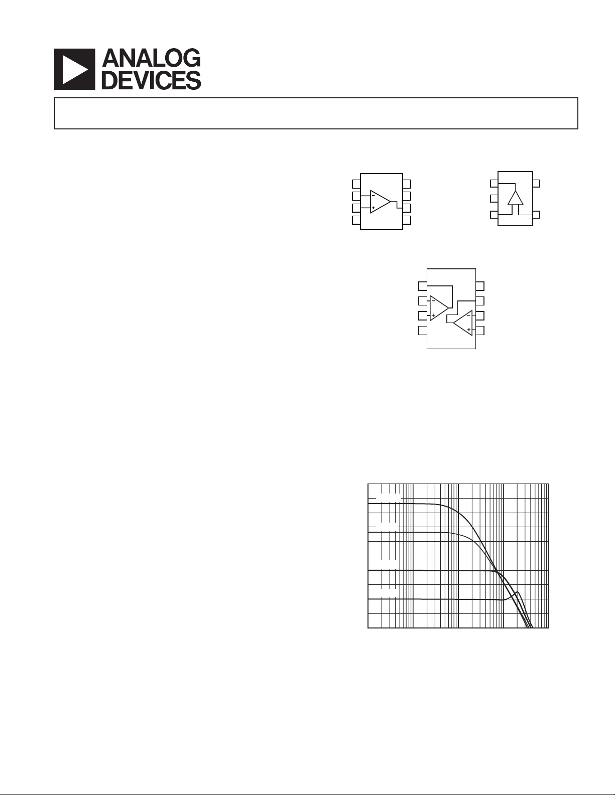
24
G = +10
21
18
15
G = +5
12
9
G = +2
GAIN – dB
6
3
G = +1
0
–3
–6
0.1 1000110100
FREQUENCY – MHz
REV. F
Information furnished by Analog Devices is believed to be accurate and
reliable. However, no responsibility is assumed by Analog Devices for its
use, nor for any infringements of patents or other rights of third parties that
may result from its use. No license is granted by implication or otherwise
under any patent or patent rights of Analog Devices. Trademarks and
registered trademarks are the property of their respective owners.
Figure 1. Small Signal Frequency Response for
Various Gains, V
One Technology Way, P.O. Box 9106, Norwood, MA 02062-9106, U.S.A.
Tel: 781/329-4700 www.analog.com
Fax: 781/326-8703 © 2004 Analog Devices, Inc. All rights reserved.
= 500 mV p-p, VS = ±5 V
OUT
Page 2

AD8038/AD8039–SPECIFICATIONS
(TA = 25ⴗC, VS = ⴞ5 V, RL = 2 k⍀, Gain = +1, unless otherwise noted.)
Parameter Conditions Min Typ Max Unit
DYNAMIC PERFORMANCE
–3 dB Bandwidth G = +1, VO = 0.5 V p-p 300 350 MHz
G = +2, V
G = +1, V
Bandwidth for 0.1 dB Flatness G = +2, V
Slew Rate G = +1, V
= 0.5 V p-p 175 MHz
O
= 2 V p-p 100 MHz
O
= 0.2 V p-p 45 MHz
O
= 2 V Step, RL = 2 kΩ 400 425 V/µs
O
Overdrive Recovery Time G = +2, 1 V Overdrive 50 ns
Settling Time to 0.1% G = +2, VO = 2 V Step 18 ns
NOISE/HARMONIC PERFORMANCE
SFDR
Second Harmonic f
= 1 MHz, VO = 2 V p-p, RL = 2 kΩ –90 dBc
C
Third Harmonic fC = 1 MHz, VO = 2 V p-p, RL = 2 kΩ –92 dBc
Second Harmonic f
Third Harmonic f
= 5 MHz, VO = 2 V p-p, RL = 2 kΩ –65 dBc
C
= 5 MHz, VO = 2 V p-p, RL = 2 kΩ –70 dBc
C
Crosstalk, Output-to-Output (AD8039) f = 5 MHz, G = +2 –70 dB
Input Voltage Noise f = 100 kHz 8 nV/√Hz
Input Current Noise f = 100 kHz 600 fA/√Hz
DC PERFORMANCE
Input Offset Voltage 0.5 3 mV
Input Offset Voltage Drift 4.5 µV/°C
Input Bias Current 400 750 nA
Input Bias Current Drift 3nA/°C
Input Offset Current 25 ± nA
Open-Loop Gain VO = ±2.5 V 70 dB
INPUT CHARACTERISTICS
Input Resistance 10 MΩ
Input Capacitance 2pF
Input Common-Mode Voltage Range R
Common-Mode Rejection Ratio V
= 1 kΩ±4V
L
= ±2.5 V 61 67 dB
CM
OUTPUT CHARACTERISTICS
DC Output Voltage Swing RL = 2 kΩ, Saturated Output ±4V
Capacitive Load Drive 30% Overshoot, G = +2 20 pF
POWER SUPPLY
Operating Range 3.0 12 V
Quiescent Current per Amplifier 1.0 1.5 mA
Power Supply Rejection Ratio – Supply –71 –77 dB
+ Supply –64 –70 dB
POWER-DOWN DISABLE*
Turn-On Time 180 ns
Turn-Off Time 700 ns
Disable Voltage—Part is OFF +V
Disable Voltage—Part is ON +V
– 4.5 V
S
– 2.5 V
S
Disabled Quiescent Current 0.2 mA
Disabled In/Out Isolation f = 1 MHz –60 dB
*Only available in AD8038 SOIC-8 package.
Specifications subject to change without notice.
–2–
REV. F
Page 3

AD8038/AD8039
SPECIFICATIONS
(TA = 25ⴗC, VS = 5 V, RL = 2 k⍀ to VS/2, Gain = +1, unless otherwise noted.)
Parameter Conditions Min Typ Max Unit
DYNAMIC PERFORMANCE
–3 dB Bandwidth G = +1, VO = 0.2 V p-p 275 300 MHz
G = +2, V
G = +1, V
Bandwidth for 0.1 dB Flatness G = +2, V
Slew Rate G = +1, V
= 0.2 V p-p 150 MHz
O
= 2 V p-p 30 MHz
O
= 0.2 V p-p 45 MHz
O
= 2 V Step, RL = 2 kΩ 340 365 V/µs
O
Overdrive Recovery Time G = +2, 1 V Overdrive 50 ns
Settling Time to 0.1% G = +2, VO = 2 V Step 18 ns
NOISE/HARMONIC PERFORMANCE
SFDR
Second Harmonic f
Third Harmonic f
Second Harmonic f
= 1 MHz, VO = 2 V p-p, RL = 2 kΩ –82 dBc
C
= 1 MHz, VO = 2 V p-p, RL = 2 kΩ –79 dBc
C
= 5 MHz, VO = 2 V p-p, RL = 2 kΩ –60 dBc
C
Third Harmonic fC = 5 MHz, VO = 2 V p-p, RL = 2 kΩ –67 dBc
Crosstalk, Output-to-Output f = 5 MHz, G = +2 –70 dB
Input Voltage Noise f = 100 kHz 8 nV/√Hz
Input Current Noise f = 100 kHz 600 fA/√Hz
DC PERFORMANCE
Input Offset Voltage 0.8 3 mV
Input Offset Voltage Drift 3 µV/°C
Input Bias Current 400 750 nA
Input Bias Current Drift 3nA/°C
Input Offset Current 30 ± nA
Open-Loop Gain VO = ±2.5 V 70 dB
INPUT CHARACTERISTICS
Input Resistance 10 MΩ
Input Capacitance 2pF
Input Common-Mode Voltage Range R
= 1 kΩ 1.0–4.0 V
L
Common-Mode Rejection Ratio VCM = ±1 V 59 65 dB
OUTPUT CHARACTERISTICS
DC Output Voltage Swing RL = 2 kΩ, Saturated Output 0.9–4.1 V
Capacitive Load Drive 30% Overshoot 20 pF
POWER SUPPLY
Operating Range 3 12 V
Quiescent Current per Amplifier 0.9 1.5 mA
Power Supply Rejection Ratio –65 –71 dB
POWER-DOWN DISABLE*
Turn-On Time 210 ns
Turn-Off Time 700 ns
Disable Voltage—Part is OFF +V
Disable Voltage—Part is ON +V
– 4.5 V
S
– 2.5 V
S
Disabled Quiescent Current 0.2 mA
Disabled In/Out Isolation f = 1 MHz –60 dB
*Only available in AD8038 SOIC-8 package.
Specifications subject to change without notice.
REV. F
–3–
Page 4
AD8038/AD8039
ABSOLUTE MAXIMUM RATINGS*
Supply Voltage . . . . . . . . . . . . . . . . . . . . . . . . . . . . . . . . . 12.6 V
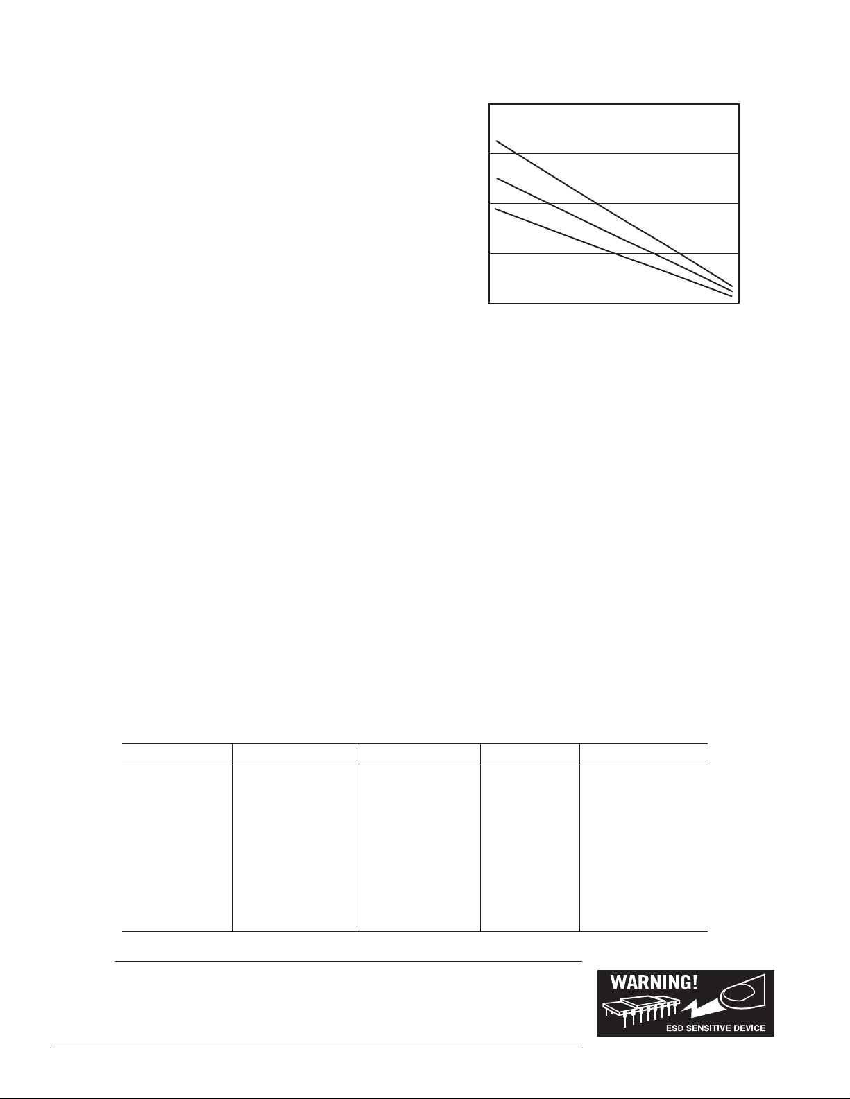
Power Dissipation . . . . . . . . . . . . . . . . . . . . . . . . . . See Figure 2
Common-Mode Input Voltage . . . . . . . . . . . . . . . . . . . . . . . ±V
S
Differential Input Voltage . . . . . . . . . . . . . . . . . . . . . . . . . . ±4 V
Storage Temperature . . . . . . . . . . . . . . . . . . . . –65°C to +125°C
Operating Temperature Range . . . . . . . . . . . . . –40°C to +85°C
Lead Temperature Range (Soldering 10 sec) . . . . . . . . . . . 300°C
*Stresses above those listed under Absolute Maximum Ratings may cause perma-
nent damage to the device. This is a stress rating only; functional operation of the
device at these or any other conditions above those indicated in the operational
section of this specification is not implied. Exposure to absolute maximum rating
conditions for extended periods may affect device reliability.
MAXIMUM POWER DISSIPATION
The maximum safe power dissipation in the AD8038/AD8039
package is limited by the associated rise in junction temperature
) on the die. The plastic encapsulating the die will locally reach
(T
J
the junction temperature. At approximately 150°C, which is the
glass transition temperature, the plastic will change its properties.
Even temporarily exceeding this temperature limit may change the
stresses that the package exerts on the die, permanently shifting the
parametric performance of the AD8038/AD8039. Exceeding a
junction temperature of 175°C for an extended period of time can
result in changes in the silicon devices, potentially causing failure.
The still-air thermal properties of the package and PCB (
ambient temperature (T
) determine the junction temperature of the die. The junction
(P
D
), and total power dissipated in the package
A
),
JA
temperature can be calculated as follows:
TT P
=+ ×
ADAJ
θ
()
J
The power dissipated in the package (PD) is the sum of the quiescent
power dissipation and the power dissipated in the package due to the
load drive for all outputs. The quiescent power is the voltage between
the supply pins (V
ing the load (R
/2 ⫻ I
is V
S
in the load (V
) multiplied by the quiescent current (IS). Assum-
S
) is referenced to midsupply, then the total drive power
L
some of which is dissipated in the package and some
OUT,
⫻ I
OUT
). The difference between the total drive
OUT
power and the load power is the drive power dissipated in the package.
= quiescent power + (total drive power – load power)
P
D
PVI V/V/R – V /R
=×
[]
DSS S OUT L OUT L
+
[]
×
2
()
()
2
[]
ORDERING GUIDE
2.0
1.5
SOIC-8
1.0
0.5
MAXIMUM POWER DISSIPATION – W
0
–55
SOT-23-8
SC70-5
–25 5 35 65 95 125
AMBIENT TEMPERATURE – ⴗC
Figure 2. Maximum Power Dissipation vs.
Temperature for a 4-Layer Board
RMS output voltages should be considered. If RL is referenced to VS–,as
⫻ I
in single-supply operation, then the total drive power is V
S
OUT
.
If the rms signal levels are indeterminate, consider the worst case,
when V
= VS /4 for RL to midsupply:
OUT
PVI V/4 /R
=×
()
DSS S2L
+
()
In single-supply operation with RL referenced to VS–, worst case is
= VS /2.
V
OUT
Airflow will increase heat dissipation, effectively reducing
. Also,
JA
more metal directly in contact with the package leads from metal
traces, through-holes, ground, and power planes will reduce the
.
JA
Care must be taken to minimize parasitic capacitances at the input
leads of high speed op amps as discussed in the board layout section.
Figure 2 shows the maximum safe power dissipation in the package
versus the ambient temperature for the SOIC-8 (125°C/W), SC70-5
(210°C/W), and SOT-23-8 (160°C/W) package on a JEDEC standard
4-layer board.
values are approximations.
JA
OUTPUT SHORT CIRCUIT
Shorting the output to ground or drawing excessive current from
the AD8038/AD8039 will likely cause a catastrophic failure.
Model Temperature Range Package Description Package Outline Branding Information
AD8038AR –40°C to +85°C 8-Lead SOIC R-8
AD8038AR-REEL –40°C to +85°C 8-Lead SOIC R-8
AD8038AR-REEL7 –40°C to +85°C 8-Lead SOIC R-8
AD8038AKS-R2 –40°C to +85°C 5-Lead SC70 KS-5 HUA
AD8038AKS-REEL –40°C to +85°C 5-Lead SC70 KS-5 HUA
AD8038AKS-REEL7 –40°C to +85°C 5-Lead SC70 KS-5 HUA
AD8039AR –40°C to +85°C 8-Lead SOIC R-8
AD8039AR-REEL –40°C to +85°C 8-Lead SOIC R-8
AD8039AR-REEL7 –40°C to +85°C 8-Lead SOIC R-8
AD8039ART-R2 –40°C to +85°C 8-Lead SOT-23 RT-8 HYA
AD8039ART-REEL –40°C to +85°C 8-Lead SOT-23 RT-8 HYA
AD8039ART-REEL7 –40°C to +85°C 8-Lead SOT-23 RT-8 HYA
CAUTION
ESD (electrostatic discharge) sensitive device. Electrostatic charges as high as 4000 V readily
accumulate on the human body and test equipment and can discharge without detection.
Although the AD8038/AD8039 features proprietary ESD protection circuitry, permanent damage
may occur on devices subjected to high energy electrostatic discharges. Therefore, proper ESD
precautions are recommended to avoid performance degradation or loss of functionality.
–4–
REV. F
Page 5

Typical Performance Characteristics–AD8038/AD8039
(Default Conditions: ⴞ5 V, CL = 5 pF, G = ⴙ2, RG = RF = 1 k⍀, RL = 2 k⍀, VO = 2 V p-p, Frequency = 1 MHz, TA = 25ⴗC.)
24
G = +10
21
18
G = +5
15
12
9
G = +2
6
GAIN – dB
3
G = +1
0
–3
–6
0.1 1000
110100
FREQUENCY – MHz
TPC 1. Small Signal Frequency
Response for Various Gains,
= 500 mV p-p
V
OUT
7
6
5
4
3
GAIN – dB
2
1
0
0.1 1000110100
RL = 500⍀
RL = 1k⍀
FREQUENCY – MHz
RL = 2k⍀
TPC 4. Small Signal Frequency
Response for Various R
= 5 V, V
V
S
= 500 mV p-p
OUT
LOAD
,
7
6
5
4
3
GAIN – dB
2
1
0
0.1 1000110100
VS = ⴞ5V
FREQUENCY – MHz
VS = ⴞ1.5V
VS = ⴞ2.5V
TPC 2. Small Signal Frequency
Response for Various Supplies,
= 500 mV p-p
V
OUT
8
7
6
5
4
GAIN – dB
3
2
1
0
0.1
110100
FREQUENCY – MHz
RL = 2k⍀
RL = 500⍀
RL = 1k⍀
TPC 5. Large Signal Frequency
Response for Various R
= 3 V p-p, VS = 5 V
V
OUT
LOAD
,
7
6
5
4
3
GAIN – dB
2
1
0
0.1 1000110100
RL = 500⍀
RL = 1k⍀
FREQUENCY – MHz
RL = 2k⍀
TPC 3. Small Signal Frequency
Response for Various R
= ±5 V, V
V
S
8
7
6
5
4
GAIN – dB
3
2
1
0
0.1
= 500 mV p-p
OUT
RL = 2k⍀
RL = 500⍀
RL = 1k⍀
110100
FREQUENCY – MHz
LOAD
,
TPC 6. Large Signal Frequency
Response for Various R
= 4 V p-p, VS = ±5 V
V
OUT
LOAD
,
5
4
3
2
1
0
–1
GAIN – dB
–2
–3
–4
–5
110100
CL = 15pF
CL = 10pF
CL = 5pF
FREQUENCY – MHz
TPC 7. Small Signal Frequency
Response for Various C
V
= 500 mV p-p, VS = ±5 V,
OUT
LOAD
G = +1
REV. F
2
1
0
–1
–2
GAIN – dB
–3
–4
–5
–6
0.1 1000110100
V
= 200mV
OUT
V
= 1V
OUT
V
= 500mV
OUT
V
= 2V
OUT
FREQUENCY – MHz
TPC 9. Frequency Response for
Various Output Voltage Levels
1000
7
5
3
1
GAIN – dB
–1
–3
–5
110100
CL = 15pF
CL = 10pF
CL = 5pF
1000
FREQUENCY – MHz
TPC 8. Small Signal Frequency
,
Response for Various C
V
= 500 mV p-p, VS = 5 V,
OUT
+1
G =
LOAD
,
–5–
Page 6

AD8038/AD8039
80
70
60
50
40
30
20
OPEN-LOOP GAIN – dB
0
–10
–20
0.01100.1 1 10 100 1000
PHASE
GAIN
FREQUENCY – MHz
180
135
90
45
PHASE – Degrees
0
–45
TPC 10. Open-Loop Gain and
Phase,
–45
–50
–55
–60
–65
–70
–75
–80
HARMONIC DISTORTION – dBc
–85
–90
= ±5 V
VS
RL = 500⍀ HD2
RL = 500⍀ HD3
RL = 2k⍀ HD3
RL = 2k⍀ HD2
18
2 34567
FREQUENCY – MHz
910
TPC 13. Harmonic Distortion vs.
Frequency for Various Loads,
V
S
= 5 V, V
= 2 V p-p, G = +2
OUT
9
6
3
GAIN – dB
0
–3
0.1 1000110100
FREQUENCY – MHz
–40ⴗC
+25ⴗC
+85ⴗC
TPC 11. Frequency Response
vs. Temperature, Gain = +2,
= ±5 V, V
V
S
–50
G = +2 HD2
–60
–70
–80
–90
HARMONIC DISTORTION – dBc
–100
18
234567
= 2 V p-p
OUT
G = +1 HD2
G = +1 HD3
FREQUENCY – MHz
G = +2 HD3
910
TPC 14. Harmonic Distortion vs.
Frequency for Various Gains,
= ±5 V, V
V
S
= 2 V p-p
OUT
–50
–55
–60
–65
–70
–75
–80
HARMONIC DISTORTION – dBc
–85
–90
RL = 500⍀ HD2
RL = 500⍀ HD3
RL = 2k⍀ HD2
18
234567
FREQUENCY – MHz
RL = 2k⍀ HD3
910
TPC 12. Harmonic Distortion vs.
Frequency for Various Loads,
V
= ±5 V, V
S
–50
G = +2 HD2
–60
–70
–80
–90
HARMONIC DISTORTION – dBc
–100
18
234567
= 2 V p-p, G = +2
OUT
G = +1 HD2
G = +1 HD3
FREQUENCY – MHz
G = +2 HD3
910
TPC 15. Harmonic Distortion vs.
Frequency for Various Gains,
V
S
= 5 V, V
= 2 V p-p
OUT
–40
10MHz HD2
–50
10MHz HD3
–60
–70
–80
–90
HARMONIC DISTORTION – dBc
–100
1
1MHz HD3
1MHz HD2
234
AMPLITUDE – V p-p
5MHz HD2
5MHz HD3
TPC 16. Harmonic Distortion vs.
V
Amplitude for Various
OUT
Frequencies,
VS = ±5 V, G = +2
–45
10MHz HD2
–55
10MHz HD3
–65
–75
–85
HARMONIC DISTORTION – dBc
–95
1.0
1.5 2.0 2.5 3.0
5MHz HD2
5MHz HD3
1MHz HD3
1MHz HD2
AMPLITUDE – V p-p
TPC 17. Harmonic Distortion vs.
Amplitude for Various Frequencies,
VS = 5 V, G = +2
1000
100
10
VOLTA G E NOISE – nV/ Hz
1
10
FREQUENCY – Hz
10M100k1k100 10k 1M 100M
TPC 18. Input Voltage Noise vs.
Frequency
–6–
REV. F
Page 7

100000
10000
1000
NOISE – fA/ Hz
RL = 500⍀
RL = 2k⍀
AD8038/AD8039
RL = 500⍀
RL = 2k⍀
100
100 1000 10000 100000 1M
10
FREQUENCY – Hz
TPC 19. Input Current Noise vs.
Frequency
CL = 25pF WITH
R
= 19.6⍀
SNUB
CL = 5pF
CL = 10pF
50mV/DIV 5ns/DIV
TPC 22. Small Signal Transient
Response for Various Capacitive
Loads, VS= 5 V
50mV/DIV 5ns/DIV
TPC 20. Small Signal Transient
Response for Various R
LOAD
,
VS= 5 V
CL = 25pF WITH
R
= 19.6⍀
SNUB
= 5pF
C
L
CL = 10pF
50mV/DIV 5ns/DIV
TPC 23. Small Signal Transient
Response for Various Capacitive
Loads, VS= ±5 V
50mV/DIV 5ns/DIV
TPC 21. Small Signal Transient
Response for Various R
LOAD
,
VS= ±5 V
RL = 500⍀ RL = 2k⍀
2.5V
500mV/DIV
5ns/DIV
TPC 24. Large Signal Transient
Response for Various R
LOAD
,
VS= 5 V
RL = 500⍀
1V/DIV
RL = 2k⍀
5ns/DIV
TPC 25. Large Signal Transient
Response for Various R
= ±5 V
V
S
LOAD
,
CL = 25pF
CL = 5pF
2.5V
500mV/DIV
5ns/DIV
TPC 26. Large Signal Transient
Response for Various Capacitive
Loads, VS = 5 V
CL = 10pF
CL = 5pF
500mV/DIV
5ns/DIV
TPC 27. Large Signal Transient
Response for Various Capacitive
Loads, VS = ±5 V
REV. F
–7–
Page 8

AD8038/AD8039
FREQUENCY – MHz
IMPEDANCE – ⍀
0.1
0.01 0.1 1 10 100 1000
VS = ⴞ5V
VS = +5V
1
10
100
1000
IN
OUT
2V/DIV
TPC 28. Input Overdrive
Recovery, Gain = +1
–10
–20
–30
–40
–50
–60
–70
CROSSTALK – dB
–80
–90
–100
0.1 1000110
SIDE B
FREQUENCY – MHz
50ns/DIV
SIDE A
100
IN
INPUT 1V/DIV
OUTPUT 2V/DIV
OUT
TPC 29. Output Overdrive
Recovery, Gain = +2
–10
–20
–30
–40
–50
CMRR – dB
–60
–70
–80
VS = +5V
VS = ⴞ5V
1 100010 100
FREQUENCY – MHz
50ns/DIV
2mV/DIV
ERROR
VOLTAGE
+0.1%
0
–0.1%
t = 0
V
IN
0.5V/DIV 5ns/DIV
TPC 30. 0.1% Settling Time
V
= 2 V p-p
OUT
VS = ⴞ5V
G = +2
= 2V p-p
V
OUT
TPC 31. AD8039 Crosstalk,
VIN = 1 V p-p, Gain = +1
10
0
–10
–20
–30
–40
–50
PSRR – dB
–60
–70
–80
–90
0.01 10000.1 10 1001
–PSRR
+PSRR
FREQUENCY – MHz
TPC 34. PSRR vs. Frequency
TPC 32. CMRR vs. Frequency,
VIN = 1 V p-p
9
8
7
6
5
– p-p
4
OUT
V
3
2
1
0
0 100 400
VS = ⴞ5V
VS = +5V
200 300 500
R
– ⍀
LOAD
TPC 35. Output Swing vs.
Load Resistance
TPC 33. Output Impedance vs.
Frequency
1.25
1.00
0.75
0.50
SUPPLY CURRENT – mA
0.25
0
0
246810
SUPPLY VOLTAGE – V
TPC 36. AD8038 Supply
Current vs. Supply Voltage
12
–8–
REV. F
Page 9

AD8038/AD8039
0
–10
–20
–30
–40
–50
ISOLATION – dB
–60
–70
–80
–90
0.1 10001.0 10 100
FREQUENCY – MHz
TPC 37. AD8038 Input-Output Isolation (G = +2,
RL = 2 kΩ, VS = ±5 V
LAYOUT, GROUNDING, AND BYPASSING
CONSIDERATIONS
Disable
The AD8038 in the SOIC-8 package provides a disable feature. This feature disables the input from the output (see TPC 37 for input-output isolation) and reduces the quiescent current from typically 1 mA to 0.2 mA. When the DISABLE node is pulled below 4.5 V from the positive supply rail, the part becomes disabled. In order to enable the part, the DISABLE node needs to be pulled up to above 2.5 V below the positive rail.
Power Supply Bypassing
Power supply pins are actually inputs, and care must be taken
so that a noise-free stable dc voltage is applied. The purpose of
bypass capacitors is to create low impedances from the supply to
ground at all frequencies, thereby shunting or filtering a majority
of the noise.
Decoupling schemes are designed to minimize the bypassing
impedance at all frequencies with a parallel combination of capacitors. 0.01 µF or 0.001 µF (X7R or NPO) chip capacitors are
critical and should be as close as possible to the amplifier package. Larger chip capacitors, such as the 0.1 µF capacitor, can be
shared among a few closely spaced active components in the same
signal path. A 10 µF tantalum capacitor is less critical for high
frequency bypassing and, in most cases, only one per board is
needed at the supply inputs.
Grounding
A ground plane layer is important in densely packed PC boards to
spread the current minimizing parasitic inductances. However,
an understanding of where the current flows in a circuit is critical
to implementing effective high speed circuit design. The length
of the current path is directly proportional to the magnitude of
parasitic inductances, and thus the high frequency impedance of
the path. High speed currents in an inductive ground return will
create an unwanted voltage noise.
The length of the high frequency bypass capacitor leads are most
critical. A parasitic inductance in the bypass grounding will work
against the low impedance created by the bypass capacitor. Place
the ground leads of the bypass capacitors at the same physical
location. Because load currents flow from the supplies as well, the
ground for the load impedance should be at the same physical
location as the bypass capacitor grounds. For the larger value
capacitors, which are intended to be effective at lower frequencies,
the current return path distance is less critical.
REV. F
–9–
Input Capacitance
Along with bypassing and ground, high speed amplifiers can be
sensitive to parasitic capacitance between the inputs and ground.
A few pF of capacitance will reduce the input impedance at high
frequencies, in turn increasing the amplifiers’ gain, causing peaking of the frequency response, or even oscillations if severe enough.
It is recommended that the external passive components that
are connected to the input pins be placed as close as possible to
the inputs to avoid parasitic capacitance. The ground and power
planes must be kept at a distance of at least 0.05 mm from the
input pins on all layers of the board.
Output Capacitance
To a lesser extent, parasitic capacitances on the output can cause
peaking of the frequency response. There are two methods to
minimize this effect.
1. Put a small value resistor in series with the output to isolate
the load capacitor from the amp’s output stage; see TPCs 7,
8, 22, and 23.
2. Increase the phase margin with higher noise gains or add a pole
with a parallel resistor and capacitor from –IN to the output.
Input-to-Output Coupling
The input and output signal traces should not be parallel to
minimize capacitive coupling between the inputs and outputs,
avoiding any positive feedback.
APPLICATIONS
Low Power ADC Driver
1k⍀
+5V
0.1F10F
1k⍀
V
IN
0V
1k⍀
1k⍀
1k⍀
8
3
2
6
5
–5V
1k⍀
1k⍀
4
1
7
0.1F
AD8039
10F
1k⍀
50⍀
50⍀
2.5V
0.1F 10F
3V
REF
VINA
AD9203
VINB
Figure 3. Schematic to Drive AD9203 with the AD8039
Differential A/D Driver
The AD9203 is a low power (125 mW on a 5 V supply) 40 MSPS
10-bit converter. This represents a breakthrough in power/speed
for ADCs. As such, the low power, high performance AD8039
is an appropriate choice of amplifier to drive it.
In low supply voltage applications, differential analog inputs
are needed to increase the dynamic range of the ADC inputs.
Differential driving can also reduce second and other even-order
distortion products. The AD8039 can be used to make a
dc-coupled, single-ended-to-differential driver for one of these
ADCs. Figure 3 is a schematic of such a circuit for driving an
AD9203, a 10-bit, 40 MSPS ADC.
Page 10

AD8038/AD8039
The AD9203 works best when the common-mode voltage at the
input is at the midsupply or 2.5 V. The output stage design of
the AD8039 makes it ideal for driving these types of ADCs.
In this circuit, one of the op amps is configured in the inverting
mode, while the other is in the noninverting mode. However, to
provide better bandwidth matching, each op amp is configured
for a noise gain of +2. The inverting op amp is configured for a
gain of –1, while the noninverting op amp is configured for a
gain of +2. Each has a very similar ac response. The input signal
to the noninverting op amp is divided by 2 to normalize its
voltage level and make it equal to the inverting output.
The outputs of the op amps are centered at 2.5 V, which is the
midsupply level of the ADC. This is accomplished by first taking
the 2.5 V reference output of the ADC and dividing it by 2 with
a pair of 1 kΩ resistors. The resulting 1.25 V is applied to each
op amp’s positive input. This voltage is then multiplied by the
gain of the op amps to provide a 2.5 V level at each output.
Low Power Active Video Filter
Some composite video signals derived from a digital source
contain clock feedthrough that can limit picture quality. Active
filters made from op amps can be used in this application, but
they will consume 25 mW to 30 mW for each channel. In
power-sensitive applications, this can be too much, requiring
the use of passive filters that can create impedance matching
problems when driving any significant load.
The AD8038 can be used to make an effective low-pass active
filter that consumes one-fifth of the power consumed by an
active filter made from an op amp. Figure 4 shows a circuit that
uses an AD8038 to create a single ±2.5 V supply, three-pole
Sallen-Key filter. This circuit uses a single RC pole in front of a
standard two-pole active section.
R
680pF
+2.5V
R3
R1
200⍀
V
IN
R4
49.9⍀
R2
499⍀
C1
100pF
49.9⍀
AD8038
C3
33pF
–2.5V
1⍀
0.1F
0.1F
F
10F
V
OUT
R5
75⍀
10F
Figure 4. Low-Pass Filter for Video
Figure 5 shows the frequency response of this filter. The response
is down 3 dB at 6 MHz, so it passes the video band with little
attenuation. The rejection at 27 MHz is 45 dB, which provides
more than a factor of 100 in suppression of the clock components
at this frequency.
10
0
–10
–20
–30
GAIN – dB
–40
–50
–60
0.1
110100
FREQUENCY – MHz
Figure 5. Video Filter Response
–10–
REV. F
Page 11

OUTLINE DIMENSIONS
AD8038/AD8039
8-Lead Standard Small Outline Package [SOIC]
(R-8)
Dimensions shown in millimeters and (inches)
5.00 (0.1968)
4.80 (0.1890)
4.00 (0.1574)
3.80 (0.1497)
0.25 (0.0098)
0.10 (0.0040)
COPLANARITY
0.10
CONTROLLING DIMENSIONS ARE IN MILLIMETERS; INCH DIMENSIONS
(IN PARENTHESES) ARE ROUNDED-OFF MILLIMETER EQUIVALENTS FOR
REFERENCE ONLY AND ARE NOT APPROPRIATE FOR USE IN DESIGN
85
1.27 (0.0500)
SEATING
PLANE
COMPLIANT TO JEDEC STANDARDS MS-012AA
BSC
6.20 (0.2440)
5.80 (0.2284)
41
1.75 (0.0688)
1.35 (0.0532)
0.51 (0.0201)
0.31 (0.0122)
0.25 (0.0098)
0.17 (0.0067)
0.50 (0.0196)
0.25 (0.0099)
8ⴗ
0ⴗ
1.27 (0.0500)
0.40 (0.0157)
5-Lead Thin Shrink Small Outline Transistor Package [SC70]
8-Lead Small Outline Transistor Package [SOT-23]
1.60 BSC
PIN 1
ⴛ 45ⴗ
INDICATOR
1.30
1.15
0.90
0.15 MAX
(KS-5)
Dimensions shown in millimeters
(RT-8)
Dimensions shown in millimeters
2.90 BSC
7
2
1.95
BSC
5 6
4
2.80 BSC
0.65 BSC
1.45 MAX
SEATING
PLANE
0.22
0.08
8
1 3
0.38
0.22
COMPLIANT TO JEDEC STANDARDS MO-178BA
ⴗ
8
ⴗ
4
ⴗ
0
0.60
0.45
0.30
1.25 BSC
1.00
0.90
0.70
0.10 MAX
2.00 BSC
0.30
0.15
4
3
0.65 BSC
2.10 BSC
1.10 MAX
SEATING
PLANE
2
5
1
PIN 1
0.10 COPLANARITY
COMPLIANT TO JEDEC STANDARDS MO-203AA
0.22
0.08
0.46
0.36
0.26
REV. F
–11–
Page 12

AD8038/AD8039
Revision History
Location Page
8/04–Data Sheet Changed from REV. E to REV. F.
Changes to Figure 4 . . . . . . . . . . . . . . . . . . . . . . . . . . . . . . . . . . . . . . . . . . . . . . . . . . . . . . . . . . . . . . . . . . . . . . . . . . . . . . . . . . . . . 10
8/03–Data Sheet Changed from REV. D to REV. E.
Change to TPC 34 . . . . . . . . . . . . . . . . . . . . . . . . . . . . . . . . . . . . . . . . . . . . . . . . . . . . . . . . . . . . . . . . . . . . . . . . . . . . . . . . . . . . . . 8
7/03–Data Sheet Changed from REV. C to REV. D.
Changes to ORDERING GUIDE . . . . . . . . . . . . . . . . . . . . . . . . . . . . . . . . . . . . . . . . . . . . . . . . . . . . . . . . . . . . . . . . . . . . . . . . . . . 4
Updated TPC 35 Caption . . . . . . . . . . . . . . . . . . . . . . . . . . . . . . . . . . . . . . . . . . . . . . . . . . . . . . . . . . . . . . . . . . . . . . . . . . . . . . . . . 8
6/03–Data Sheet Changed from REV. B to REV. C.
Updated CONNECTION DIAGRAMS . . . . . . . . . . . . . . . . . . . . . . . . . . . . . . . . . . . . . . . . . . . . . . . . . . . . . . . . . . . . . . . . . . . . . . 1
Updated ORDERING GUIDE . . . . . . . . . . . . . . . . . . . . . . . . . . . . . . . . . . . . . . . . . . . . . . . . . . . . . . . . . . . . . . . . . . . . . . . . . . . . . 4
Updated OUTLINE DIMENSIONS . . . . . . . . . . . . . . . . . . . . . . . . . . . . . . . . . . . . . . . . . . . . . . . . . . . . . . . . . . . . . . . . . . . . . . . 11
5/02–Data Sheet Changed from REV. A to REV. B.
Add part number AD8038 . . . . . . . . . . . . . . . . . . . . . . . . . . . . . . . . . . . . . . . . . . . . . . . . . . . . . . . . . . . . . . . . . . . . . . . UNIVERSAL
Changes to Product Title . . . . . . . . . . . . . . . . . . . . . . . . . . . . . . . . . . . . . . . . . . . . . . . . . . . . . . . . . . . . . . . . . . . . . . . . . . . . . . . . . . 1
Changes to FEATURES . . . . . . . . . . . . . . . . . . . . . . . . . . . . . . . . . . . . . . . . . . . . . . . . . . . . . . . . . . . . . . . . . . . . . . . . . . . . . . . . . . 1
Changes to PRODUCT DESCRIPTION . . . . . . . . . . . . . . . . . . . . . . . . . . . . . . . . . . . . . . . . . . . . . . . . . . . . . . . . . . . . . . . . . . . . . 1
Changes to CONNECTION DIAGRAM . . . . . . . . . . . . . . . . . . . . . . . . . . . . . . . . . . . . . . . . . . . . . . . . . . . . . . . . . . . . . . . . . . . . . 1
Update to SPECIFICATIONS . . . . . . . . . . . . . . . . . . . . . . . . . . . . . . . . . . . . . . . . . . . . . . . . . . . . . . . . . . . . . . . . . . . . . . . . . . . . . 2
Update to MAXIMUM POWER DISSIPATION . . . . . . . . . . . . . . . . . . . . . . . . . . . . . . . . . . . . . . . . . . . . . . . . . . . . . . . . . . . . . . . 4
Update to OUTPUT SHORT CIRCUIT . . . . . . . . . . . . . . . . . . . . . . . . . . . . . . . . . . . . . . . . . . . . . . . . . . . . . . . . . . . . . . . . . . . . . 4
Update to ORDERING GUIDE . . . . . . . . . . . . . . . . . . . . . . . . . . . . . . . . . . . . . . . . . . . . . . . . . . . . . . . . . . . . . . . . . . . . . . . . . . . . 4
Change to FIGURE 2 . . . . . . . . . . . . . . . . . . . . . . . . . . . . . . . . . . . . . . . . . . . . . . . . . . . . . . . . . . . . . . . . . . . . . . . . . . . . . . . . . . . . 4
Change to TPC 2 . . . . . . . . . . . . . . . . . . . . . . . . . . . . . . . . . . . . . . . . . . . . . . . . . . . . . . . . . . . . . . . . . . . . . . . . . . . . . . . . . . . . . . . 5
Change to TPC 18 . . . . . . . . . . . . . . . . . . . . . . . . . . . . . . . . . . . . . . . . . . . . . . . . . . . . . . . . . . . . . . . . . . . . . . . . . . . . . . . . . . . . . . 6
Change to TPC 27 . . . . . . . . . . . . . . . . . . . . . . . . . . . . . . . . . . . . . . . . . . . . . . . . . . . . . . . . . . . . . . . . . . . . . . . . . . . . . . . . . . . . . . 7
Change to TPC 29 . . . . . . . . . . . . . . . . . . . . . . . . . . . . . . . . . . . . . . . . . . . . . . . . . . . . . . . . . . . . . . . . . . . . . . . . . . . . . . . . . . . . . . 8
Change to TPC 30 . . . . . . . . . . . . . . . . . . . . . . . . . . . . . . . . . . . . . . . . . . . . . . . . . . . . . . . . . . . . . . . . . . . . . . . . . . . . . . . . . . . . . . 8
Change to TPC 31 . . . . . . . . . . . . . . . . . . . . . . . . . . . . . . . . . . . . . . . . . . . . . . . . . . . . . . . . . . . . . . . . . . . . . . . . . . . . . . . . . . . . . . 8
Added TPC 36 . . . . . . . . . . . . . . . . . . . . . . . . . . . . . . . . . . . . . . . . . . . . . . . . . . . . . . . . . . . . . . . . . . . . . . . . . . . . . . . . . . . . . . . . . 8
Added TPC 37 . . . . . . . . . . . . . . . . . . . . . . . . . . . . . . . . . . . . . . . . . . . . . . . . . . . . . . . . . . . . . . . . . . . . . . . . . . . . . . . . . . . . . . . . . 9
Edits to Low Power Active Video Filter . . . . . . . . . . . . . . . . . . . . . . . . . . . . . . . . . . . . . . . . . . . . . . . . . . . . . . . . . . . . . . . . . . . . . . 10
Change to Figure 4 . . . . . . . . . . . . . . . . . . . . . . . . . . . . . . . . . . . . . . . . . . . . . . . . . . . . . . . . . . . . . . . . . . . . . . . . . . . . . . . . . . . . . 10
4/02–Data Sheet Changed from REV. 0 to REV. A.
Changes to FEATURES . . . . . . . . . . . . . . . . . . . . . . . . . . . . . . . . . . . . . . . . . . . . . . . . . . . . . . . . . . . . . . . . . . . . . . . . . . . . . . . . . . 1
Update SPECIFICATIONS . . . . . . . . . . . . . . . . . . . . . . . . . . . . . . . . . . . . . . . . . . . . . . . . . . . . . . . . . . . . . . . . . . . . . . . . . . . . . 2, 3
Edits to TPC 19 . . . . . . . . . . . . . . . . . . . . . . . . . . . . . . . . . . . . . . . . . . . . . . . . . . . . . . . . . . . . . . . . . . . . . . . . . . . . . . . . . . . . . . . . 7
C02951–0–8/04(F)
–12–
REV. F
 Loading...