

Page 1
Low Cost, 80 MHz
www.BDTIC.com/ADI
FEATURES
FET input amplifier
1 pA typical input bias current
Very low cost
High speed
80 MHz, −3 dB bandwidth (G = +1)
80 V/μs slew rate (G = +2)
Low noise
11 nV/√Hz (f = 100 kHz)
0.7 fA/√Hz (f = 100 kHz)
Wide supply voltage range: 5 V to 24 V
Low offset voltage: 1 mV typical
Single-supply and rail-to-rail output
High common-mode rejection ratio: −100 dB
Low power: 3.3 mA/amplifier typical supply current
No phase reversal
Small packaging: 8-lead SOIC, 8-lead SOT-23, and 5-lead SC70
APPLICATIONS
Instrumentation
Filters
Level shifting
Buffering
GENERAL DESCRIPTION
The AD8033/AD8034 FastFET™ amplifiers are voltage feedback
amplifiers with FET inputs, offering ease of use and excellent
performance. The AD8033 is a single amplifier and the AD8034
is a dual amplifier. The AD8033/AD8034 FastFET op amps in
Analog Devices, Inc., proprietary XFCB process offer significant
performance improvements over other low cost FET amps, such
as low noise (11 nV/√Hz and 0.7 fA/√Hz) and high speed (80 MHz
bandwidth and 80 V/µs slew rate).
With a wide supply voltage range from 5 V to 24 V and fully
operational on a single supply, the AD8033/AD8034 amplifiers
work in more applications than similarly priced FET input
amplifiers. In addition, the AD8033/AD8034 have rail-to-rail
outputs for added versatility.
Despite their low cost, the amplifiers provide excellent overall
performance. They offer a high common-mode rejection of
−100 dB, low input offset voltage of 2 mV maximum, and low
noise of 11 nV/√Hz.
FastFET Op Amps
AD8033/AD8034
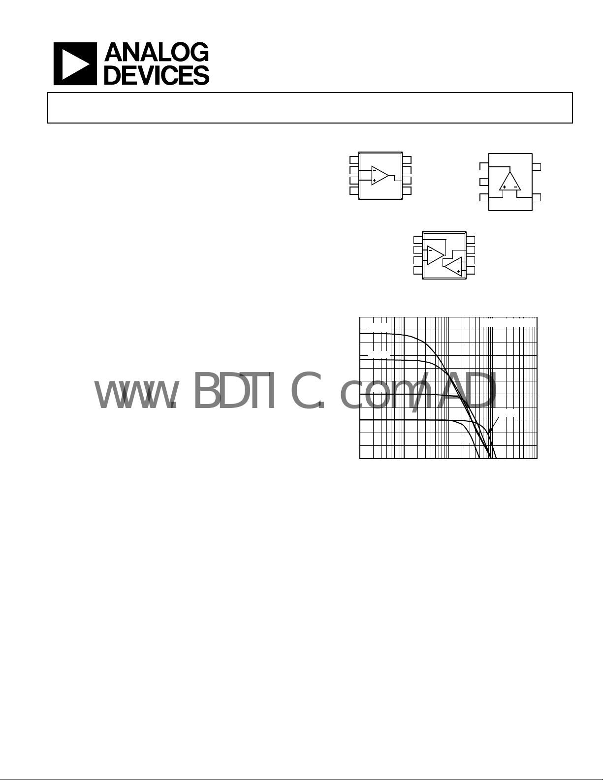
CONNECTION DIAGRAMS
1
NC
AD8033
2
–IN
+IN
3
–V
4
S
NC = NO CONNECT
Figure 1. 8-Lead SOIC (R) Figure 2. 5-Lead SC70 (KS)
Figure 3. 8-Lead SOIC (R) and 8-Lead SOT-23 (RJ)
24
G = +10
21
18
G = +5
15
12
9
G = +2
6
GAIN (dB)
3
0
–3
–6
–9
The AD8033/AD8034 amplifiers only draw 3.3 mA/amplifier of
quiescent current while having the capability of delivering up to
40 mA of load current.
The AD8033 is available in a small package 8-lead SOIC and a
small package 5-lead SC70. The AD8034 is also available in a
small package 8-lead SOIC and a small package 8-lead SOT-23.
They are rated to work over the industrial temperature range of
−40°C to +85°C without a premium over commercial grade
products.
8
V
OUT1
–IN1
+IN1
–V
1
NC
7
+V
V
6
NC
5
S
S
OUT
02924-001
1
2
3
4
AD8034
G = –1
10
FREQUENCY (MHz)
V
OUT
–V
+IN
8
7
6
5
S
+V
V
–IN2
+IN2
1
2
3
S
OUT2
V
OUT
1000.1
AD8033
02924-003
= 200mV p-p
G = +1
Figure 4. Small Signal Frequency Response
5
4
1000
+V
–IN
S
02924-004
2924-002
Rev. D
Information furnished by Analog Devices is believed to be accurate and reliable. However, no
responsibility is assumed by Analog Devices for its use, nor for any infringements of patents or other
rights of third parties that may result from its use. Specifications subject to change without notice. No
license is granted by implication or otherwise under any patent or patent rights of Analog Devices.
Trademarks and registered trademarks are the property of their respective owners.
One Technology Way, P.O. Box 9106, Norwood, MA 02062-9106, U.S.A.
Tel: 781.329.4700 www.analog.com
Fax: 781.461.3113 ©2002–2008 Analog Devices, Inc. All rights reserved.
Page 2

AD8033/AD8034
www.BDTIC.com/ADI
TABLE OF CONTENTS
Features .............................................................................................. 1
Applications ....................................................................................... 1
General Description ......................................................................... 1
Connection Diagrams ...................................................................... 1
Revision History ............................................................................... 2
Specifications ..................................................................................... 3
Absolute Maximum Ratings ............................................................ 6
Maximum Power Dissipation ..................................................... 6
Output Short Circuit .................................................................... 6
ESD Caution .................................................................................. 6
Typical Performance Characteristics ............................................. 7
Test Circuits ..................................................................................... 14
Theory of Operation ...................................................................... 16
Output Stage Drive and Capacitive Load Drive ..................... 16
REVISION HISTORY
9/08—Rev. C to Rev. D
Deleted Usable Input Range Parameter, Table 1 ........................... 3
Deleted Usable Input Range Parameter, Table 2 ........................... 4
Deleted Usable Input Range Parameter, Table 3 ........................... 5
4/08—Rev. B to Rev. C
Changes to Format ............................................................. Universal
Changes to Features and General Description ............................. 1
Changes to Figure 13 Caption and Figure 14 Caption ................ 8
Changes to Figure 22 and Figure 23 ............................................... 9
Changes to Figure 25 and Figure 28 ............................................. 10
Changes to Input Capacitance Section ........................................ 18
Changes to Active Filters Section ................................................. 21
Changes to Outline Dimensions ................................................... 23
Changes to Ordering Guide .......................................................... 24
2/03—Rev. A to Rev. B
Changes to Features .......................................................................... 1
Changes to Connection Diagrams ................................................. 1
Changes to Specifications ................................................................ 2
Changes to Absolute Maximum Ratings ....................................... 4
Replaced TPC 31............................................................................. 11
Changes to TPC 35 ......................................................................... 11
Changes to Test Circuit 3 ............................................................... 12
Updated Outline Dimensions ....................................................... 19
Input Overdrive .......................................................................... 16
Input Impedance ........................................................................ 16
Thermal Considerations ............................................................ 16
Layout, Grounding, and Bypassing Considerations .................. 18
Bypassing ..................................................................................... 18
Grounding ................................................................................... 18
Leakage Currents ........................................................................ 18
Input Capacitance ...................................................................... 18
Applications Information .............................................................. 19
High Speed Peak Detector ........................................................ 19
Active Filters ............................................................................... 20
Wideband Photodiode Preamp ................................................ 21
Outline Dimensions ....................................................................... 23
Ordering Guide .......................................................................... 24
8/02—Rev. 0 to Rev. A
Added AD8033 ................................................................... Universal
V
= 2 V p-p Deleted from Default Conditions ......... Universal
OUT
Added SOIC-8 (R) and SC70 (KS) .................................................. 1
Edits to General Description Section ............................................. 1
Changes to Specifications ................................................................. 2
New Figure 2 ...................................................................................... 5
Edits to Maximum Power Dissipation Section .............................. 5
Changes to Ordering Guide ............................................................. 5
Change to TPC 3 ............................................................................... 6
Change to TPC 6 ............................................................................... 6
Change to TPC 9 ............................................................................... 7
New TPC 16 ....................................................................................... 8
New TPC 17 ....................................................................................... 8
New TPC 31 .................................................................................... 11
New TPC 35 .................................................................................... 11
New Test Circuit 9 .......................................................................... 13
SC70 (KS) Package Added ............................................................ 19
Rev. D | Page 2 of 24
Page 3

AD8033/AD8034
www.BDTIC.com/ADI
SPECIFICATIONS
TA = 25°C, VS = ±5 V, RL = 1 kΩ, gain = +2, unless otherwise noted.
Table 1.
Parameter Conditions Min Typ Max Unit
DYNAMIC PERFORMANCE
−3 dB Bandwidth G = +1, V
G = +2, V
G = +2, V
Input Overdrive Recovery Time −6 V to +6 V input 135 ns
Output Overdrive Recovery Time −3 V to +3 V input, G = +2 135 ns
Slew Rate (25% to 75%) G = +2, V
Settling Time to 0.1% G = +2, V
G = +2, V
NOISE/HARMONIC PERFORMANCE
Distortion fC = 1 MHz, V
Second Harmonic RL = 500 Ω −82 dBc
R
Third Harmonic RL = 500 Ω −70 dBc
R
Crosstalk, Output-to-Output f = 1 MHz, G = +2 −86 dB
Input Voltage Noise f = 100 kHz 11 nV/√Hz
Input Current Noise f = 100 kHz 0.7 fA/√Hz
DC PERFORMANCE
Input Offset Voltage VCM = 0 V 1 2 mV
T
Input Offset Voltage Match 2.5 mV
Input Offset Voltage Drift 4 27 V/°C
Input Bias Current 1.5 11 pA
T
Open-Loop Gain V
INPUT CHARACTERISTICS
Common-Mode Input Impedance 1000||2.3 GΩ||pF
Differential Input Impedance 1000||1.7 GΩ||pF
Input Common-Mode Voltage Range
FET Input Range −5.0 to +2.2 V
Common-Mode Rejection Ratio VCM = −3 V to +1.5 V −89 −100 dB
OUTPUT CHARACTERISTICS
Output Voltage Swing ±4.75 ±4.95 V
Output Short-Circuit Current 40 mA
Capacitive Load Drive 30% overshoot, G = +1, V
POWER SUPPLY
Operating Range 5 24 V
Quiescent Current per Amplifier 3.3 3.5 mA
Power Supply Rejection Ratio VS = ±2 V −90 −100 dB
= 1 kΩ −85 dBc
L
= 1 kΩ −81 dBc
L
MIN
MIN
OUT
= 0.2 V p-p 65 80 MHz
OUT
= 0.2 V p-p 30 MHz
OUT
= 2 V p-p 21 MHz
OUT
= 4 V step 55 80 V/µs
OUT
= 2 V step 95 ns
OUT
= 8 V step 225 ns
OUT
= 2 V p-p
OUT
− T
3.5 mV
MAX
− T
50 pA
MAX
= ± 3 V 89 92 dB
= 400 mV p-p 35 pF
OUT
Rev. D | Page 3 of 24
Page 4

AD8033/AD8034
www.BDTIC.com/ADI
TA = 25°C, VS = 5 V, RL = 1 k, gain = +2, unless otherwise noted.
Table 2.
Parameter Conditions Min Typ Max Unit
DYNAMIC PERFORMANCE
−3 dB Bandwidth G = +1, V
G = +2, V
G = +2, V
Input Overdrive Recovery Time −3 V to +3 V input 180 ns
Output Overdrive Recovery Time −1.5 V to +1.5 V input, G = +2 200 ns
Slew Rate (25% to 75%) G = +2, V
Settling Time to 0.1% G = +2, V
NOISE/HARMONIC PERFORMANCE
Distortion fC = 1 MHz, V
Second Harmonic RL = 500 Ω −80 dBc
R
= 1 kΩ −84 dBc
L
Third Harmonic RL = 500 Ω −70 dBc
R
= 1 kΩ −80 dBc
L
Crosstalk, Output to Output f = 1 MHz, G = +2 −86 dB
Input Voltage Noise f = 100 kHz 11 nV/√Hz
Input Current Noise f = 100 kHz 0.7 fA/√Hz
DC PERFORMANCE
Input Offset Voltage VCM = 0 V 1 2 mV
T
MIN
Input Offset Voltage Match 2.5 mV
Input Offset Voltage Drift 4 30 V/°C
Input Bias Current 1 10 pA
T
Open-Loop Gain V
MIN
OUT
INPUT CHARACTERISTICS
Common-Mode Input Impedance 1000||2.3 GΩ||pF
Differential Input Impedance 1000||1.7 GΩ||pF
Input Common-Mode Voltage Range
FET Input Range 0 to 2.0 V
Common-Mode Rejection Ratio VCM = 1.0 V to 2.5 V −80 −100 dB
OUTPUT CHARACTERISTICS
Output Voltage Swing RL = 1 kΩ 0.16 to 4.83 0.04 to 4.95 V
Output Short-Circuit Current 30 mA
Capacitive Load Drive 30% overshoot, G = +1, V
POWER SUPPLY
Operating Range 5 24 V
Quiescent Current per Amplifier 3.3 3.5 mA
Power Supply Rejection Ratio VS = ±1 V −80 −100 dB
= 0.2 V p-p 70 80 MHz
OUT
= 0.2 V p-p 32 MHz
OUT
= 2 V p-p 21 MHz
OUT
= 4 V step 55 70 V/s
OUT
= 2 V step 100 ns
OUT
= 2 V p-p
OUT
− T
3.5 mV
MAX
− T
50 pA
MAX
= 0 V to 3 V 87 92 dB
= 400 mV p-p 25 pF
OUT
Rev. D | Page 4 of 24
Page 5

AD8033/AD8034
www.BDTIC.com/ADI
TA = 25°C, VS = ±12 V, RL = 1 k, gain = +2, unless otherwise noted.
Table 3.
Parameter Conditions Min Typ Max Unit
DYNAMIC PERFORMANCE
−3 dB Bandwidth G = +1, V
G = +2, V
G = +2, V
Input Overdrive Recovery Time −13 V to +13 V input 100 ns
Output Overdrive Recovery Time −6.5 V to +6.5 V input, G = +2 100 ns
Slew Rate (25% to 75%) G = +2, V
Settling Time to 0.1% G = +2, V
G = +2, V
NOISE/HARMONIC PERFORMANCE
Distortion fC = 1 MHz, V
Second Harmonic RL = 500 Ω −80 dBc
R
= 1 kΩ −82 dBc
L
Third Harmonic RL = 500 Ω −70 dBc
R
= 1 kΩ −82 dBc
L
Crosstalk, Output to Output f = 1 MHz, G = +2 −86 dB
Input Voltage Noise f = 100 kHz 11 nV/√Hz
Input Current Noise f = 100 kHz 0.7 fA/√Hz
DC PERFORMANCE
Input Offset Voltage VCM = 0 V 1 2 mV
T
MIN
Input Offset Voltage Match 2.5 mV
Input Offset Voltage Drift 4 24 V/°C
Input Bias Current 2 12 pA
T
Open-Loop Gain V
MIN
OUT
INPUT CHARACTERISTICS
Common-Mode Input Impedance 1000||2.3 GΩ||pF
Differential Input Impedance 1000||1.7 GΩ||pF
Input Common-Mode Voltage Range
FET Input Range −12.0 to +9.0 V
Common-Mode Rejection Ratio VCM = ±5 V −92 −100 dB
OUTPUT CHARACTERISTICS
Output Voltage Swing ±11.52 ±11.84 V
Output Short-Circuit Current 60 mA
Capacitive Load Drive 30% overshoot, G = +1 35 pF
POWER SUPPLY
Operating Range 5 24 V
Quiescent Current per Amplifier 3.3 3.5 mA
Power Supply Rejection Ratio VS = ±2 V −85 −100 dB
= 0.2 V p-p 65 80 MHz
OUT
= 0.2 V p-p 30 MHz
OUT
= 2 V p-p 21 MHz
OUT
= 4 V step 55 80 V/s
OUT
= 2 V step 90 ns
OUT
= 10 V step 225 ns
OUT
= 2 V p-p
OUT
− T
3.5 mV
MAX
− T
50 pA
MAX
= ±8 V 88 96 dB
Rev. D | Page 5 of 24
Page 6
AD8033/AD8034
www.BDTIC.com/ADI
ABSOLUTE MAXIMUM RATINGS
Table 4.
Parameter Rating
Supply Voltage 26.4 V
Power Dissipation See Figure 5
Common-Mode Input Voltage 26.4 V
Differential Input Voltage 1.4 V
Storage Temperature Range −65°C to +125°C
Operating Temperature Range −40°C to +85°C
Lead Temperature (Soldering 10 sec) 300°C
Stresses above those listed under Absolute Maximum Ratings
may cause permanent damage to the device. This is a stress
rating only; functional operation of the device at these or any
other conditions above those indicated in the operational
section of this specification is not implied. Exposure to absolute
maximum rating conditions for extended periods may affect
device reliability.
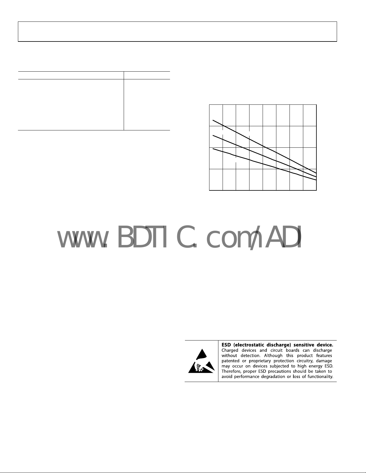
MAXIMUM POWER DISSIPATION
The maximum safe power dissipation in the AD8033/AD8034
packages is limited by the associated rise in junction temperature
(T
) on the die. The plastic that encapsulates the die locally
J
reaches the junction temperature. At approximately 150°C,
which is the glass transition temperature, the plastic changes its
properties. Even temporarily exceeding this temperature limit
can change the stresses that the package exerts on the die,
permanently shifting the parametric performance of the AD8033/
AD8034. Exceeding a junction temperature of 175°C for an
extended period can result in changes in silicon devices, potentially
causing failure.
OUT
),
JA
)
S
,
The still-air thermal properties of the package and PCB (θ
ambient temperature (T
package (P
) determine the junction temperature of the die.
D
), and the total power dissipated in the
A
The junction temperature can be calculated as
T
= TA + (PD × θJA)
J
P
is the sum of the quiescent power dissipation and the power
D
dissipated in the package due to the load drive for all outputs.
The quiescent power is the voltage between the supply pins (V
times the quiescent current (I
referenced to midsupply, the total drive power is V
). Assuming the load (RL) is
S
/2 × I
S
some of which is dissipated in the package and some in the load
(V
× I
OUT
). The difference between the total drive power and
OUT
the load power is the drive power dissipated in the package
= Quiescent Power + (Total Drive Power − Load Power)
P
D
= [VS × IS] + [(VS/2) × (V
P
D
OUT/RL
)] − [V
RMS output voltages should be considered. If R
, as in single-supply operation, the total drive power is
to −V
S
V
× I
.
S
OUT
2
/RL]
OUT
is referenced
L
If the rms signal levels are indeterminate, consider the worst case,
when V
In single-supply operation with R
is V
= VS/4 for RL to midsupply
OUT
= (VS × IS) + (VS/4)2/RL
P
D
referenced to VS−, worst case
L
= VS/2.
OUT
2.0
1.5
SOT-23-8
1.0
SC70-5
0.5
MAXIMUM POW ER DISSIPATION (W )
0
–60 –20–40 10060 80
Figure 5. Maximum Power Dissipation vs.
Ambient Temperature for a 4-Layer Board
SOIC-8
40020
AMBIENT TEM PERATURE (°C)
02924-005
Airflow increases heat dissipation, effectively reducing θJA. In
addition, more metal directly in contact with the package leads
from metal traces, through holes, ground, and power planes
reduces the θ
. Care must be taken to minimize parasitic
JA
capacitances at the input leads of high speed op amps as discussed
in the Layout, Grounding, and Bypassing Considerations section.
Figure 5 shows the maximum power dissipation in the package
vs. the ambient temperature for the 8-lead SOIC (125°C/W),
5-lead SC70 (210°C/W), and 8-lead SOT-23 (160°C/W) packages
on a JEDEC standard 4-layer board. θ
values are approximations.
JA
OUTPUT SHORT CIRCUIT
Shorting the output to ground or drawing excessive current for
the AD8033/AD8034 will likely cause catastrophic failure.
ESD CAUTION
Rev. D | Page 6 of 24
Page 7
AD8033/AD8034
www.BDTIC.com/ADI
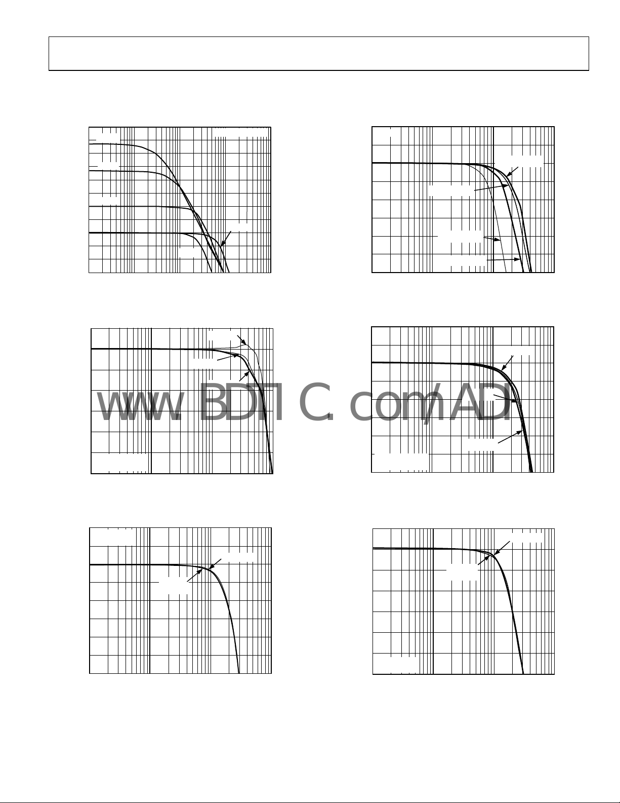
TYPICAL PERFORMANCE CHARACTERISTICS
Default conditions: VS = ±5 V, CL = 5 pF, RL = 1 k, TA = 25°C.
24
G = +10
21
18
G = +5
15
12
9
G = +2
6
GAIN (dB)
3
0
–3
–6
–9
G = –1
10
FREQUENCY (MHz)
V
= 200mV p-p
OUT
1000.1 1
G = +1
Figure 6. Small Signal Frequency Response for Various Gains
1
0
–1
–2
–3
GAIN (dB)
–4
–5
G = +1
= 200mV p-p
V
OUT
–6
FREQUENCY (MHz )
V
S
VS= +5V
=±5V
VS= ±12V
Figure 7. Small Signal Frequency Response for Various Supplies
(See Figure 44)
2
G = +1
= 2V
p-p
V
OUT
1
0
–1
–2
GAIN (dB)
–3
–4
–5
–6
VS=±5V
= +5V
V
S
FREQUE NCY (MHz )
VS= ±12V
10
Figure 8. Large Signal Frequency Response for Various Supplies
(See Figure 44)
1000
02924-006
1000.1 1 10
02924-007
1000.1 1
02924-008
8
G = +2
7
V
= 0.2V p-p
6
5
4
GAIN (dB)
3
2
1
0
V
= 1V p-p
OUT
V
= 4V p-p
OUT
V
= 2V p-p
OUT
FREQUENCY (MHz )
OUT
1000.1 1 10
02924-009
Figure 9. Frequency Response for Various Output Amplitudes (See Figure 45)
8
7
6
5
V
4
GAIN (dB)
3
2
1
G = +2
V
= 200mV p-p
OUT
0
FREQUENCY (MHz)
S
VS=
VS= +5V
=±5V
±12V
1000.1 1 10
02924-010
Figure 10. Small Signal Frequency Response for Various Supplies
(See Figure 45)
7
6
=±5V
V
5
4
3
GAIN (dB)
2
1
G = +2
V
= 2V p-p
OUT
0
S
V
= +5V
S
FREQUENCY (MHz )
V
= ±12V
S
1000.1 1 10
02924-011
Figure 11. Large Signal Frequency Response for Various Supplies
(See Figure 45)
Rev. D | Page 7 of 24
Page 8
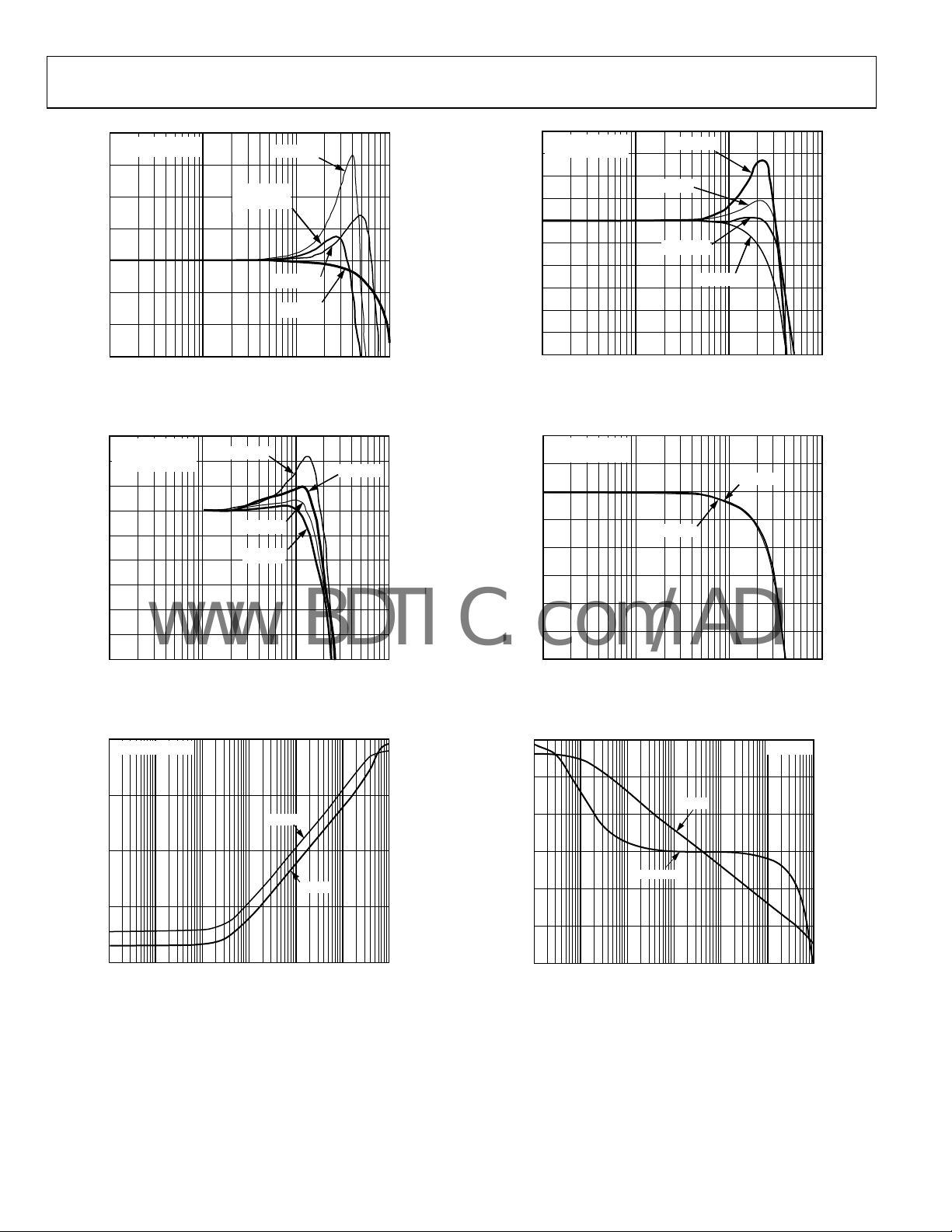
AD8033/AD8034
(
www.BDTIC.com/ADI
8
V
= 200mV p-p
OUT
G = +1
6
4
2
0
GAIN (dB)
–2
–4
–6
110
FREQUENCY (MHz)
CL= 100pF
R
SNUB
CL= 100pF
= 25Ω
CL= 33pF
CL= 2pF
1000.1
02924-012
Figure 12. Small Signal Frequency Response for Various CL (See Figure 44)
9
V
= 200mV p-p
OUT
= 3kΩ
R
F
8
G = +2
7
6
5
4
GAIN (dB)
3
2
1
0
CF= 0pF
CF= 1pF
CF= 1.5pF
CF= 2pF
110
FREQUENCY (MHz )
1000.1
02924-013
Figure 13. Small Signal Frequency Response for Various CF (See Figure 45)
100
V
= 200mV p-p
OUT
10
V
= 200mV p-p
OUT
G = +2
9
8
7
6
5
4
GAIN (dB)
3
2
1
0
CL= 100pF
CL= 51pF
CL= 33pF
CL= 2pF
1
FREQUENCY (MHz)
10
1000.1
02924-015
Figure 15. Small Signal Frequency Response for Various CL (See Figure 45)
8
V
= 200mV p-p
OUT
G = +2
7
6
5
4
GAIN (dB)
3
2
1
0
RL= 500Ω
FREQUENCY (MHz )
R
= 1kΩ
L
1000.1 1 10
02924-016
Figure 16. Small Signal Frequency Response for Various RL (See Figure 45)
100
VS = ±12V
180
80
10
Ω)
1
IMPEDANCE
0.1
0.01
100 1k 10k 100k 1M 10M 100M
FREQUENCY (Hz)
G = +2
G = +1
Figure 14. Output Impedance vs. Frequency (See Figure 47)
2924-014
60
40
GAIN (dB)
20
0
–20
100 1k 10k 100k 1M 10M 100M
PHASE
FREQUENCY (Hz)
Figure 17. Open-Loop Response
Rev. D | Page 8 of 24
GAIN
150
120
90
60
30
0
PHASE (Degrees)
02924-017
Page 9

AD8033/AD8034
–
–
√
–
–
www.BDTIC.com/ADI
–50
40
G = +2
HD3 RL = 500
Ω
40
–50
–60
–70
–80
–90
DISTORTION (dBc)
–100
–110
–120
HD3 RL = 1k
HD2 RL = 1k
FREQUENCY (MHz)
Ω
= 500
HD2 R
Ω
Ω
L
510.1
02924-018
Figure 18. Harmonic Distortion vs. Frequency for Various Loads
(See Figure 45)
40
DISTORTI ON (dBc)
–100
–110
–120
–50
–60
–70
–80
–90
G = +2
HD2 V
= 5V
S
HD2 V
FREQUENCY (MHz)
= 24V
S
1
HD3 V
= 5V
S
HD3 VS = 24V
50.1
02924-019
Figure 19. Harmonic Distortion vs. Frequency for Various Supply Voltages
(See Figure 45)
1000
–60
DISTORT ION (dBc)
–100
–110
–120
–70
–80
–90
HD3 G = +2
HD2 G = +1
HD3 G = +1
FREQUENCY (MHz )
HD2 G = +2
50.1 1
Figure 21. Harmonic Distortion vs. Frequency for Various Gains
20
G = +2
DISTORTION (dBc)
–100
–110
–120
–30
–40
–50
–60
–70
–80
–90
HD3 V
= 20V p-p
OUT
HD2 V
OUT
= 10V p-p
OUT
= 2V p-p
FREQUENCY (MHz)
HD2 V
HD2 V
HD3 V
OUT
OUT
OUT
= 20V p-pHD3 V
= 10V p-p
= 2V p-p
50.1 1
Figure 22. Harmonic Distortion vs. Frequency for Various Amplitudes
(See Figure 45), V
80
G = +1
70
= 24 V
S
VS = +5V
POSITIVE SI DE
02924-021
02924-022
60
VS = +5V
NEGATIVE SIDE
Hz)
100
NOISE (n V/
10
100 1k 10k 100k 1M 10M 100M
FREQUENCY (Hz)
M0110
02924-020
Figure 20. Voltage Noise vs. Frequency
50
40
30
PERCENT OVERSHOOT (%)
20
10
0
10 30 50 70 90 110
VS =±5V
Figure 23. Percent Overshoot vs. Capacitive Load (See Figure 44)
Rev. D | Page 9 of 24
VS =±5V
POSITI VE SIDE
CAPACITIVE L OAD (pF)
NEGATIVE SIDE
2924-023
Page 10

AD8033/AD8034
www.BDTIC.com/ADI
G = +1
G = +1
38pF
15pF
25mV/DIV
20ns/DIV
Figure 24. Small Signal Transient Response 5 V (See Figure 44)
G = +1
V
= 20V p-p
OUT
V
= 8V p-p
OUT
V
= 2V p-p
OUT
3V/DIV
320ns/DIV
Figure 25. Large Signal Transient Response (See Figure 44)
G = –1
V
IN
V
OUT
02924-024
80mV/DIV
80ns/DIV
02924-027
Figure 27. Small Signal Transient Response ±5 V (See Figure 44)
G = +2
2924-025
3V/DIV
V
OUT
V
OUT
V
OUT
= 20V p-p
= 8V p-p
= 2V p-p
320ns/DIV
02924-028
Figure 28. Large Signal Transient Response (See Figure 45)
G = +1
V
OUT
V
IN
1.5V/DIV
Figure 26. Output Overdrive Recovery (See Figure 46)
350ns/DIV
02924-026
1.5V/DIV
Figure 29. Input Overdrive Recovery (See Figure 44)
Rev. D | Page 10 of 24
350ns/DIV
02924-029
Page 11

AD8033/AD8034
(
(
www.BDTIC.com/ADI
VIN = 1V
VIN = 1V
V
– 2V
OUT
IN
t
= 0
+0.1%
–0.1%
t
= 0
V
– 2V
OUT
IN
+0.1%
–0.1%
2mV/DIV
Figure 30. Long-Term Settling Time
0
–5
–10
–15
–20
(pA)
b
I
–25
–30
–35
–40
25 30 35 40 45 50 60 65 70 807555
BJT INPUT RANGE
42
36
30
A)
24
µ
18
b
I
12
6
0
FET INPUT RANGE
10
5
0
–5
A)
p
–10
b
I
–15
–20
–25
–30
Figure 32. I
1.5µs/DI V
+I
b
TEMPERATURE ( °C)
Figure 31. Ib vs. Temperature
+I
b
–I
b
–4–6–8–10–12 –2
COMMON-MO DE VOLTAG E (V)
vs. Common-Mode Voltage Range
b
02468 1210
02924-030
2mV/DIV
20ns/DIV
02924-033
Figure 33. 0.1% Short-Term Settling Time
7.0
6.9
6.8
–I
b
8520
02924-031
6.7
6.6
6.5
6.4
6.3
6.2
6.1
QUIESCENT S UPPLY CURRENT (mA)
6.0
5.9
–40 –20
= ±12V
V
S
= ±5V
V
S
VS = +5V
0 20406080
TEMPERATURE (°C)
02924-034
Figure 34. Quiescent Supply Current vs. Temperature for Various Supply
Voltages
4.0
3.5
–I
b
+I
b
02924-032
NORMALIZED OFFSET (mV)
3.0
2.5
2.0
1.5
1.0
0.5
–0.5
–1.0
VS = +5VVS = ±5V
0
–12 –10 –8 –6 –4 –2 0 2 4 6 8 10 12 14–14
COMMON-MO DE VOLTAGE (V)
V
S
= ±12V
02924-035
Figure 35. Input Offset Voltage vs. Common-Mode Voltage
Rev. D | Page 11 of 24
Page 12

AD8033/AD8034
–
–
www.BDTIC.com/ADI
20
–30
–40
–50
CMRR (dB)
–60
–70
–80
0.1 1 10 100
FREQUENCY (MHz)
Figure 36. CMRR vs. Frequency (See Figure 50)
1.0
0.8
VCC –V
OH
0.6
0.4
VOL – V
OUTPUT SATURATION (V)
0.2
EE
2924-036
105
100
95
90
85
80
75
OPEN-LOOP GAIN (dB)
70
65
60
–12
RL = 500Ω
RL = 1kΩ
OUTPUT VOLTAGE (V)
RL = 2kΩ
Figure 39. Open-Loop Gain vs. Output Voltage for Various R
40
–50
–60
–70
SOT-23 B/A
CROSSTALK (d B)
–80
–90
SOT-23 A/B
SOIC A/B
SOIC B/A
12–10–8–6–4–2 2468100
2924-039
L
0
10 15 20 25
I
(mA)
LOAD
Figure 37. Output Saturation Voltage vs. Load Current
0
–10
–20
–30
–40
–50
PSRR (dB)
–60
–70
–80
–90
–100
0.0001 0.001 0 .01 0.1 1 10
–PSRR
+PSRR
FREQUENCY (MHz )
Figure 38. PSRR vs. Frequency (See Figure 49 and Figure 51)
3005
100
–100
0.1
02924-037
FREQUENCY (MHz)
101
50
2924-040
Figure 40. Crosstalk (See Figure 52)
180
150
120
90
FREQUENCY
60
30
0
–1.5 –1.0 –0.5 0 0.5 1.0 1. 5
02924-038
VOS (mV)
02924-041
Figure 41. Initial Offset
Rev. D | Page 12 of 24
Page 13

AD8033/AD8034
www.BDTIC.com/ADI
V
OUT
V
OUT
1.2V/DIV
V
IN
Figure 42. G = +1 Response, V
= ±5 V
S
1µs/DIV
2924-042
1.2V/DIV
Figure 43. G = +2 Response, V
V
IN
= ±5 V
S
1µs/DIV
2924-043
Rev. D | Page 13 of 24
Page 14

AD8033/AD8034
V
V
V
www.BDTIC.com/ADI
TEST CIRCUITS
+V
S
1µF
+
10nF
IN
49.9Ω
AD8033/AD8034
10nF
1µF
–V
S
Figure 44. G = +1
R
SNUB
976Ω
C
LOAD
+
49.9Ω
V
OUT
02924-044
Figure 47. Output Impedance, G = +1
C
F
1kΩ
IN
499Ω
49.9Ω
1kΩ
R
F
+V
S
1µF
+
10nF
AD8033/AD8034
10nF
+
1µF
–V
S
Figure 45. G = +2
R
SNUB
C
976Ω
LOAD
49.9Ω
V
OUT
02924-045
Figure 48. Output Impedance, G = +2
IN
1kΩ1kΩ
+V
S
1
µF
+
10nF
AD8033/AD8034
10nF
+
1µF
–V
S
1k
Ω1kΩ
+V
S
1µF
+
10nF
AD8033/AD8034
10nF
+
1µF
–V
S
V
SINE
0.2V p-p
V
SINE
0.2V p-p
+
–
02924-047
+
–
02924-048
+V
S
1µF
+
499Ω
10nF
AD8033/AD8034
10nF
+
1µF
–V
S
976Ω
49.9
V
OUT
Ω
02924-046
Figure 46. G = −1
Rev. D | Page 14 of 24
Page 15

AD8033/AD8034
–V
p
www.BDTIC.com/ADI
+V
S
1µF
+
10nF
V
AD8033/AD8034
1V p-p
+
–
S
–VSAC
49.9Ω
OUT
02924-051
Figure 49. Negative PSRR
1kΩ 1kΩ
+V
S
V
IN
49.9
Ω
1kΩ
1kΩ
1µF
+
10nF
AD8033/AD8034
10nF
+
1µF
–V
S
976Ω
49.9Ω
TO PORT 1
+
IN
50Ω
–
TO PORT 2
V
V
OUT
02924-050
Figure 50. CMRR
1V p-
+V
–
+
AC
+V
S
49.9Ω
AD8033/AD8034
10nF
+
1µF
–V
S
Figure 51. Positive PSRR
1kΩ1kΩ
–V
S
–
499Ω
1kΩ
B
+
+V
S
–V
S
+
A
–
+V
S
Figure 52. Crosstalk
S
V
OUT
02924-049
1kΩ
499Ω
1kΩ1kΩ
02924-052
Rev. D | Page 15 of 24
Page 16

AD8033/AD8034
www.BDTIC.com/ADI
THEORY OF OPERATION
The incorporation of JFET devices into the Analog Devices
high voltage XFCB process has enabled the ability to design the
AD8033/AD8034. The AD8033/AD8034 are voltage feedback
rail-to-rail output amplifiers with FET inputs and a bipolarenhanced common-mode input range. The use of JFET devices in
high speed amplifiers extends the application space into both the
low input bias current and low distortion, high bandwidth areas.
Using N-channel JFETs and a folded cascade input topology,
the common-mode input level operates from 0.2 V below the
negative rail to within 3.0 V of the positive rail. Cascading of
the input stage ensures low input bias current over the entire
common-mode range as well as CMRR and PSRR specifications
that are above 90 dB. Additionally, long-term settling issues that
normally occur with high supply voltages are minimized as a
result of the cascading.
OUTPUT STAGE DRIVE AND CAPACITIVE LOAD DRIVE
The common emitter output stage adds rail-to-rail output
performance and is compensated to drive 35 pF (30% overshoot
at G = +1). Additional capacitance can be driven if a small snub
resistor is put in series with the capacitive load, effectively
decoupling the load from the output stage, as shown in Figure 12.
The output stage can source and sink 20 mA of current within
500 mV of the supply rails and 1 mA within 100 mV of the
supply rails.
INPUT OVERDRIVE
An additional feature of the AD8033/AD8034 is a bipolar input
pair that adds rail-to-rail common-mode input performance
specifically for applications that cannot tolerate phase inversion
problems.
Under normal common-mode operation, the bipolar input
pair is kept reversed, maintaining I
the input common-mode operation comes within 3.0 V of the
positive supply rail, I1 turns off and I4 turns on, supplying tail
current to the bipolar pair Q25 and Q27. With this configuration,
the inputs can be driven beyond the positive supply rail without
any phase inversion (see Figure 53).
at less than 1 pA. When
b
As a result of entering the bipolar mode of operation, an offset
and input bias current shift occurs (see Figure 32 and Figure 35).
After re-entering the JFET common-mode range, the amplifier
recovers in approximately 100 ns (refer to Figure 29 for input
overload behavior). Above and below the supply rails, ESD
protection diodes activate, resulting in an exponentially
increasing input bias current. If the inputs are driven well
beyond the rails, series input resistance should be included
to limit the input bias current to <10 mA.
INPUT IMPEDANCE
The input capacitance of the AD8033/AD8034 forms a pole
with the feedback network, resulting in peaking and ringing
in the overall response. The equivalent impedance of the
feedback network should be kept small enough to ensure that
the parasitic pole falls well beyond the −3 dB bandwidth of the
gain configuration being used. If larger impedance values are
desired, the amplifier can be compensated by placing a small
capacitor in parallel with the feedback resistor. Figure 13 shows
the improvement in frequency response by including a small
feedback capacitor with high feedback resistance values.
THERMAL CONSIDERATIONS
Because the AD8034 operates at up to ±12 V supplies in the
small 8-lead SOT-23 package (160°C/W), power dissipation can
easily exceed package limitations, resulting in permanent shifts
in device characteristics and even failure. Likewise, high supply
voltages can cause an increase in junction temperature even
with light loads, resulting in an input bias current and offset
drift penalty. The input bias current doubles for every 10°C
shown in Figure 31. Refer to the Maximum Power Dissipation
section for an estimation of die temperature based on load and
supply voltage.
Rev. D | Page 16 of 24
Page 17

AD8033/AD8034
V
www.BDTIC.com/ADI
V
TH
+
S
Q27
I2
Q9
R14
Q7
R3
+
V2
–
Q4
Q13
J2
D5
+IN
Q11
Q29
R7
I3
Q1
Q14
V
CC
Q28
R8
+
V4
–
V
OUT
02924-053
R2
Q6
D4
J1
–IN
I1 I4
–V
S
Q25
Figure 53. Simplified AD8033/AD8034 Input Stage
Rev. D | Page 17 of 24
Page 18

AD8033/AD8034
www.BDTIC.com/ADI
LAYOUT, GROUNDING, AND BYPASSING CONSIDERATIONS
BYPASSING
Power supply pins are actually inputs, and care must be taken
so that a noise-free stable dc voltage is applied. The purpose of
bypass capacitors is to create low impedances from the supply
to ground at all frequencies, thereby shunting or filtering a
majority of the noise. Decoupling schemes are designed to
minimize the bypassing impedance at all frequencies with a
parallel combination of capacitors. The chip capacitors, 0.01 µF
or 0.001 µF (X7R or NPO), are critical and should be placed as
close as possible to the amplifier package. Larger chip capacitors,
such as the 0.1 µF capacitor, can be shared among a few closely
spaced active components in the same signal path. The 10 µF
tantalum capacitor is less critical for high frequency bypassing, and
in most cases, only one per board is needed at the supply inputs.
GROUNDING
A ground plane layer is important in densely packed PCBs to
spread the current, thereby minimizing parasitic inductances.
However, an understanding of where the current flows in a
circuit is critical to implementing effective high speed circuit
design. The length of the current path is directly proportional
to the magnitude of the parasitic inductances and, thus, the
high frequency impedance of the path. High speed currents
in an inductive ground return create unwanted voltage noise.
The length of the high frequency bypass capacitor leads is most
critical. A parasitic inductance in the bypass grounding works
against the low impedance created by the bypass capacitor.
Place the ground leads of the bypass capacitors at the same
physical location.
Because load currents flow from the supplies as well, the ground
for the load impedance should be at the same physical location
as the bypass capacitor grounds. For the larger value capacitors
that are intended to be effective at lower frequencies, the current
return path distance is less critical.
LEAKAGE CURRENTS
Poor PCB layout, contaminants, and the board insulator material
can create leakage currents that are much larger than the input
bias currents of the AD8033/AD8034. Any voltage differential
between the inputs and nearby runs set up leakage currents
through the PCB insulator, for example, 1 V/100 G = 10 pA.
Similarly, any contaminants on the board can create significant
leakage (skin oils are a common problem). To significantly reduce
leakages, put a guard ring (shield) around the inputs and input
leads that is driven to the same voltage potential as the inputs.
This way there is no voltage potential between the inputs and
surrounding area to set up any leakage currents. For the guard
ring to be completely effective, it must be driven by a relatively
low impedance source and should completely surround the input
leads on all sides, above, and below using a multilayer board.
Another effect that can cause leakage currents is the charge
absorption of the insulator material itself. Minimizing the amount
of material between the input leads and the guard ring helps to
reduce the absorption. In addition, low absorption materials
such as Teflon® or ceramic may be necessary in some instances.
INPUT CAPACITANCE
Along with bypassing and ground, high speed amplifiers can be
sensitive to parasitic capacitance between the inputs and
ground. A few pF of capacitance reduces the input impedance at
high frequencies, in turn it increases the gain of the amplifier
and can cause peaking of the overall frequency response or even
oscillations if severe enough. It is recommended that the external
passive components that are connected to the input pins be placed
as close as possible to the inputs to avoid parasitic capacitance.
The ground and power planes must be kept at a distance of at
least 0.05 mm from the input pins on all layers of the board.
Rev. D | Page 18 of 24
Page 19

AD8033/AD8034
V
www.BDTIC.com/ADI
APPLICATIONS INFORMATION
HIGH SPEED PEAK DETECTOR
The low input bias current and high bandwidth of the AD8033/
AD8034 make the parts ideal for a fast settling, low leakage peak
detector. The classic fast-low leakage topology with a diode in
the output is limited to ~1.4 V p-p maximum in the case of the
AD8033/AD8034 because of the protection diodes across the
inputs, as shown in Figure 54.
AD8033/
V
IN
~1.4V p-p MAX
Figure 54. High Speed Peak Detector with Limited Input Range
AD8034
Using the AD8033/AD8034, a unity gain peak detector can
be constructed that captures a 300 ns pulse while still taking
advantage of the low input bias current and wide commonmode input range of the AD8033/AD8034, as shown in Figure 55.
V
OUT
02924-054
Using two amplifiers, the difference between the peak and the
current input level is forced across R2 instead of either amplifier’s
input pins. In the event of a rising pulse, the first amplifier
compensates for the drop across D2 and D3, forcing the voltage
at Node 3 equal to Node 1. D1 is off and the voltage drop across
R2 is zero. Capacitor C3 speeds up the loop by providing the
charge required by the input capacitance of the first amplifier,
helping to maintain a minimal voltage drop across R2 in the
sampling mode. A negative going edge results in D2 and D3
turning off and D1 turning on, closing the loop around the
first amplifier and forcing V
− VIN across R2. R4 makes
OUT
the voltage across D2 zero, minimizing leakage current and
kickback from D3 from affecting the voltage across C2.
The rate of the incoming edge must be limited so that the output
of the first amplifier does not overshoot the peak value of V
before the output of the second amplifier can provide negative
feedback at the summing junction of the first amplifier. This
is accomplished with the combination of R1 and C1, which
allows the voltage at Node 1 to settle to 0.1% of V
The selection of C2 and R3 is made by considering droop
rate, settling time, and kickback. R3 prevents overshoot from
occurring at Node 3. The time constants of R1, C1 and R3, C2
are roughly equal to achieve the best performance. Slower time
constants can be selected by increasing C2 to minimize droop
rate and kickback at the cost of increased settling time. R1 and
C1 should also be increased to match, reducing the incoming
pulse’s effect on kickback.
C3
10pF
in 270 ns.
IN
IN
R2
1kΩ
D1
LS4148
+V
S
R1
IN
49.9Ω
1kΩ
R5
39pF/
C1
120pF
1/2
AD8034
–V
S
Figure 55. High Speed, Unity Gain Peak Detector Using AD8034
D3
LS4148
C4
4.7pF
R4
6kΩ
D2
LS4148
C2
200Ω
+V
S
1/2
AD8034
–V
180pF/
560pF
R3
V
OUT
S
2924-056
Rev. D | Page 19 of 24
Page 20

AD8033/AD8034
www.BDTIC.com/ADI
The Sallen-Key topology is the least dependent on the active
INPUT
OUTPUT
2
1V/DIV 100n s/DIV
02924-055
Figure 56. Peak Detector Response 4 V, 300 ns Pulse
Figure 56 shows the peak detector in Figure 55 capturing a
300 ns, 4 V pulse with 10 mV of kickback and a droop rate of
5 V/s. For larger peak-to-peak pulses, increase the time constants
of R1, C1 and R3, C3 to reduce overshoot. The best droop rate
occurs by isolating parasitic resistances from Node 3, which can
be accomplished using a guard band connected to the output of the
second amplifier that surrounds its summing junction (Node 3).
Increasing both time constants by a factor of 3 permits a larger
peak pulse to be captured and increases the output accuracy.
INPUT
OUTPUT
2
1V/DIV 200ns/DIV
02924-057
Figure 57. Peak Detector Response 5 V, 1 μs Pulse
Figure 57 shows a 5 V peak pulse being captured in 1 µs with
less than 1 mV of kickback. With this selection of time constants,
up to a 20 V peak pulse can be captured with no overshoot.
ACTIVE FILTERS
The response of an active filter varies greatly depending on the
performance of the active device. Open-loop bandwidth and
gain, along with the order of the filter, determines the stop-band
attenuation as well as the maximum cutoff frequency, while
input capacitance can set a limit on which passive components
are used. Topologies for active filters are varied, and some are
more dependent on the performance of the active device than
others are.
device, requiring that the bandwidth be flat to beyond the stopband frequency because it is used simply as a gain block. In the
case of high Q filter stages, the peaking must not exceed the openloop bandwidth and the linear input range of the amplifier.
Using an AD8033/AD8034, a 4-pole cascaded Sallen-Key filter
can be constructed with f
= 1 MHz and over 80 dB of stop-band
C
attenuation, as shown in Figure 58.
C3
V
IN
4.99kΩ
R4
82pF
33pF
R1
4.22kΩ
R5
49.9Ω
C4
4.99kΩ
R2
6.49kΩ
C1
27pF
R3
C2
10pF
AD8034
1/2
AD8034
+V
1/2
–V
+V
S
–V
S
S
V
OUT
S
Figure 58. 4-Pole Cascade Sallen-Key Filter
Component values are selected using a normalized cascaded,
2-stage Butterworth filter table and Sallen-Key 2-pole active
filter equations. The overall frequency response is shown in
Figure 59.
0
–10
–20
–30
–40
–50
–60
REF LEVEL (dB)
–70
–80
–90
–100
100k
FREQUENCY (Hz)
Figure 59. 4-Pole Cascade Sallen-Key Filter Response
10M1M10k
02924-058
2924-059
Rev. D | Page 20 of 24
Page 21

AD8033/AD8034
V
I
×
www.BDTIC.com/ADI
When selecting components, the common-mode input capacitance
must be taken into consideration.
Filter cutoff frequencies can be increased beyond 1 MHz using the
AD8033/AD8034 but limited open-loop gain and input impedance
begin to interfere with the higher Q stages. This can cause early
roll-off of the overall response.
Additionally, the stop-band attenuation decreases with decreasing
open-loop gain.
Keeping these limitations in mind, a 2-pole Sallen-Key Butterworth
filter with f
= 4 MHz can be constructed that has a relatively
C
low Q of 0.707 while still maintaining 15 dB of attenuation an
octave above f
and 35 dB of stop-band attenuation. The filter
C
and response are shown in Figure 60 and Figure 61, respectively.
WIDEBAND PHOTODIODE PREAMP
Figure 62 shows an I/V converter with an electrical model of a
photodiode.
The basic transfer function is
R
V
where I
PHOTO
=
OUT
PHOTO
+
1
is the output current of the photodiode, and the
parallel combination of R
F
RsC
FF
and CF sets the signal bandwidth.
F
C
F
R
F
C
M
C
D
C
M
creates a zero
F
(45)
V
OUT
) is defined
02924-062
S
f
CR
F
RSH = 1011Ω
CR
××π
S
R
F
C3
22pF
R1
R5
49.9Ω
2.49kΩ
IN
R2
2.49kΩ
10pF
C1
Figure 60. 2-Pole Butterworth Active Filter
5
0
–5
–10
–15
–20
GAIN (dB)
–25
–30
–35
–40
–45
FREQUENCY (Hz)
Figure 61. 2-Pole Butterworth Active Filter Response
AD8033
10M
+V
S
V
OUT
–V
S
02924-060
I
PHOTO
C
S
V
B
CF + C
Figure 62. Wideband Photodiode Preamp
The stable bandwidth attainable with this preamp is a function
of R
, the gain bandwidth product of the amplifier, and the total
F
capacitance at the summing junction of the amplifier, including
C
and the amplifier input capacitance. RF and the total capacitance
S
produce a pole in the loop transmission of the amplifier that
can result in peaking and instability. Adding C
in the loop transmission that compensates for the effect of the
pole and reduces the signal bandwidth. It can be shown that the
signal bandwidth resulting in a 45°phase margin (f
by the expression
=
f
)45(
2
100M100k 1M
2924-061
where:
is the amplifier crossover frequency.
f
CR
is the feedback resistor.
R
F
is the total capacitance at the amplifier summing junction
C
S
(amplifier + photodiode + board parasitics).
The value of C
that produces f
F
(45)
is
C
=
C
F
S
2
××π
F
The frequency response in this case shows about 2 dB of
peaking and 15% overshoot. Doubling C
bandwidth in half results in a flat frequency response, with
about 5% transient overshoot.
Rev. D | Page 21 of 24
fR
CR
and cutting the
F
Page 22

AD8033/AD8034
√
www.BDTIC.com/ADI
The output noise over frequency of the preamp is shown in
Figure 63.
The pole in the loop transmission translates to a zero in the
noise gain of the amplifier, leading to an amplification of the
input voltage noise over frequency. The loop transmission zero
introduced by C
limits the amplification. The bandwidth of the
F
noise gain extends past the preamp signal bandwidth and is
eventually rolled off by the decreasing loop gain of the amplifier.
Keeping the input terminal impedances matched is recommended
to eliminate common-mode noise peaking effects that add to
the output noise.
Integrating the square of the output voltage noise spectral density
over frequency and then taking the square root results in the
total rms output noise of the preamp.
f
=
1
2πRF (CF + CS + CM + 2CD)
f2 =
Hz)
RF NOISE
VOLTAGE NOISE (nV/
f
1
VEN
2πRF C
f
=
3
(C
f
2
NOISE DUE T O AMPLIF IER
Figure 63. Photodiode Voltage Noise Contributions
1
1
F
f
CR
+ CM + 2CD + CF)/C
S
VEN (C
+ CS + CM + 2CD)/C
F
FREQUENCY (Hz)
F
f
3
F
02924-063
Rev. D | Page 22 of 24
Page 23

AD8033/AD8034
www.BDTIC.com/ADI
OUTLINE DIMENSIONS
5.00 (0.1968)
4.80 (0.1890)
4.00 (0.1574)
3.80 (0.1497)
0.25 (0.0098)
0.10 (0.0040)
COPLANARITY
0.10
CONTROLL ING DIMENSI ONS ARE IN MILLIMETERS; INCH DI MENSIONS
(IN PARENTHESES) ARE ROUNDED-OFF MILLIMETER EQUIVALENTS FOR
REFERENCE ONLY AND ARE NOT APPROPRI ATE FOR USE IN DESIGN.
85
1
1.27 (0.0500)
SEATING
PLANE
COMPLIANT TO JEDEC STANDARDS MS-012-A A
BSC
6.20 (0.2441)
5.80 (0.2284)
4
1.75 (0.0688)
1.35 (0.0532)
0.51 (0.0201)
0.31 (0.0122)
8°
0°
0.25 (0.0098)
0.17 (0.0067)
0.50 (0.0196)
0.25 (0.0099)
1.27 (0.0500)
0.40 (0.0157)
45°
012407-A
Figure 64. 8-Lead Standard Small Outline Package [SOIC_N]
Narrow Body (R-8)
Dimensions shown in millimeters and (inches)
2.20
2.00
1.80
1.35
1.25
1.15
PIN 1
1.00
0.90
0.70
0
.
1
0
M
A
X
0.10 COPLANARITY
123
0.30
0.15
COMPLIANT TO JEDEC STANDARDS MO-203-AA
45
0.65 BSC
2.40
2.10
1.80
1.10
0.80
SEATING
PLANE
0.40
0.10
0.22
0.08
0.46
0.36
0.26
Figure 65. 5-Lead Thin Shrink Small Outline Transistor Package [SC70]
(KS-5)
Dimensions shown in millimeters
2.90 BSC
2
1.95
BSC
56
0.65 BSC
2.80 BSC
1.45 MAX
SEATING
PLANE
0.22
0.08
8°
4°
0°
1.60 BSC
PIN 1
INDICATOR
1.30
1.15
0.90
0.15 MAX
847
13
0.38
0.22
COMPLIANT TO JEDEC STANDARDS MO-178-B A
Figure 66. 8-Lead Small Outline Transistor Package [SOT-23]
(RJ-8)
Dimensions shown in millimeters
Rev. D | Page 23 of 24
0.60
0.45
0.30
Page 24

AD8033/AD8034
www.BDTIC.com/ADI
ORDERING GUIDE
Model Temperature Range Package Description Package Option Branding
AD8033AR –40°C to +85°C 8-Lead SOIC_N R-8
AD8033AR-REEL –40°C to +85°C 8-Lead SOIC_N R-8
AD8033AR-REEL7 –40°C to +85°C 8-Lead SOIC_N R-8
AD8033ARZ
AD8033ARZ-REEL
AD8033ARZ-REEL7
AD8033AKS-R2 –40°C to +85°C 5-Lead SC70 KS-5 H3B
AD8033AKS-REEL –40°C to +85°C 5-Lead SC70 KS-5 H3B
AD8033AKS-REEL7 –40°C to +85°C 5-Lead SC70 KS-5 H3B
AD8033AKSZ-R2
AD8033AKSZ-REEL
AD8033AKSZ-REEL7
AD8034AR –40°C to +85°C 8-Lead SOIC_N R-8
AD8034AR-REEL7 –40°C to +85°C 8-Lead SOIC_N R-8
AD8034AR-REEL –40°C to +85°C 8-Lead SOIC_N R-8
AD8034ARZ
AD8034ARZ-REEL
AD8034ARZ-REEL7
AD8034ART-R2 –40°C to +85°C 8-Lead SOT-23 RJ-8 HZA
AD8034ART-REEL –40°C to +85°C 8-Lead SOT-23 RJ-8 HZA
AD8034ART-REEL7 –40°C to +85°C 8-Lead SOT-23 RJ-8 HZA
AD8034ARTZ-R2
AD8034ARTZ-REEL
AD8034ARTZ-REEL7
AD8034CHIPS DIE
1
Z = RoHS Compliant Part, # denotes RoHS compliant product may be top or bottom marked.
1
–40°C to +85°C 8-Lead SOIC_N R-8
1
–40°C to +85°C 8-Lead SOIC_N R-8
1
–40°C to +85°C 8-Lead SOIC_N R-8
1
–40°C to +85°C 5-Lead SC70 KS-5 H3C
1
–40°C to +85°C 5-Lead SC70 KS-5 H3C
1
–40°C to +85°C 5-Lead SC70 KS-5 H3C
1
–40°C to +85°C 8-Lead SOIC_N R-8
1
–40°C to +85°C 8-Lead SOIC_N R-8
1
–40°C to +85°C 8-Lead SOIC_N R-8
1
–40°C to +85°C 8-Lead SOT-23 RJ-8 HZA#
1
–40°C to +85°C 8-Lead SOT-23 RJ-8 HZA#
1
–40°C to +85°C 8-Lead SOT-23 RJ-8 HZA#
©2002–2008 Analog Devices, Inc. All rights reserved. Trademarks and
registered trademarks are the property of their respective owners.
D02924-0-9/08(D)
Rev. D | Page 24 of 24
 Loading...