

Page 1
Quad High Speed
R
F
R
G
R
G
R
F
V
EE
V
CC
AD8026
R
F
R
P
R
P
OUT A
–IN A
+IN A
+IN B
–IN B
OUT B
OUT D
–IN D
+IN D
+IN C
–IN C
OUT C
R
F
R
G
R
P
R
P
R
G
a
FEATURES
Voltage Feedback, Rail-to-Rail Output
Rated Settling Time to Within 0.5 V of Supply Rail
Quad High Speed Amplifier
Settling Time to 0.1% of 55 ns (4 V Swing, C
Slew Rate 135 V/ms (4 V Swing)
–3 dB Bandwidth 60 MHz
Fixed Gain Resistors for High DC Accuracy
Low Voltage Offset 0.5 mV RTO Typical
Gain Error Less than 0.05%
Low Supply Current 3.4 mA
Nominal +12 V Supply
14-Lead SOIC Package
APPLICATIONS
LCD Source Drivers
CD DVD
CDR
PRODUCT DESCRIPTION
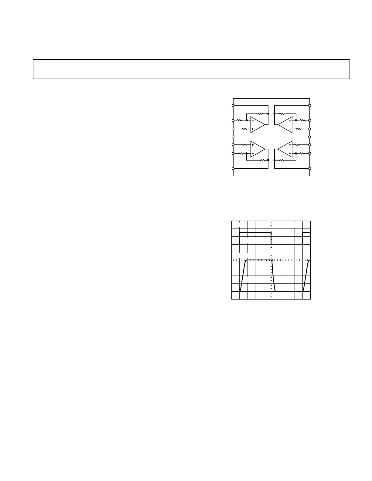
The AD8026 is a complete low cost, closed loop, voltage feedback, quad amplifier. Precision trimmed resistors set a fixed R
ratio of 5/3 to a typical gain accuracy of 0.02%. Manufac-
R
G
tured on ADI’s proprietary XFCB high speed bipolar process,
which enables the output drivers to settle to within 0.1% within
55 ns into a 100 pF load (4 V swing) and drive output voltages
to rated settling time to within 0.5 V from the rail. The typical
3 dB bandwidth is 60 MHz, at G = +2.67. The AD8026 is
laser trimmed to produce both exceptional offset and gain
performance.
The low settling time, high slew rate, low offset and rail-to-rail
output voltage drive capability makes the AD8026 ideal for
driving LCD displays.
The AD8026 is available in a 14-lead SOIC package.
= 100 pF)
L
/
F
FUNCTIONAL BLOCK DIAGRAM
RL = 10kV
50ns/DIV
1V/DIV
1V/DIV
INPUT
OUTPUT
VIN = 1.5V
V
= 4V
OUT
Figure 1. 4 V Step Response
Amplifier
AD8026
REV. 0
Information furnished by Analog Devices is believed to be accurate and
reliable. However, no responsibility is assumed by Analog Devices for its
use, nor for any infringements of patents or other rights of third parties
which may result from its use. No license is granted by implication or
otherwise under any patent or patent rights of Analog Devices.
One Technology Way, P.O. Box 9106, Norwood, MA 02062-9106, U.S.A.
Tel: 781/329-4700 World Wide Web Site: http://www.analog.com
Fax: 781/326-8703 © Analog Devices, Inc., 1998
Page 2

(@ +258C, VS = 66 V, RI = 500 V, RL = 10 kV, RF = 5K, RG = 3K Noninverting
AD8026–SPECIFICATIONS
Configuration, T
= 08C, T
MIN
= +708C, unless otherwise noted.)
MAX
Parameter Conditions Min Typ Max Units
DYNAMIC PERFORMANCE
–3 dB Small Signal Bandwidth V
Bandwidth for 0.1 dB Flatness V
Slew Rate V
Full Power Response V
Settling Time to 0.1% V
= 50 mV rms
IN
= 1 kΩ 20 60 MHz
R
L
= 50 mV rms
IN
= 1 kΩ 12 MHz
R
L
= 4 V Step 135 V/µs
O
= 2 V p-p 10 MHz
O
= 4 V Step, CL = 100 pF,
O
R
= 50 Ω 55 ns
S
NOISE/DISTORTION PERFORMANCE
Total Harmonic Distortion f
Voltage Noise (RTO)
1
Crosstalk, Output to Output f = 5 MHz, V
Differential Gain Error NTSC R
Differential Phase Error NTSC R
DC PERFORMANCE
RTO Offset Voltage
2
= 5 MHz, VO = 2 V p-p,
C
= 1 kΩ –60 dBc
R
L
f = 10 kHz 67 nV/√Hz
= 2 V p-p,
= 1 kΩ –80 dB
R
L
O
= 1 kΩ 0.02 %
L
= 1 kΩ 0.02 Degrees
L
VIN = 0 V 0.5 5.5 mV
to T
T
MIN
MAX
6mV
RTO Offset Drift 10 µV/°C
+Input Bias Current 0.6 1.6 µA
Closed-Loop Gain Error
Gain Matching Channel-to-Channel, R
3
R
= 10 kΩ, –2.67 < V
L
to T
T
MIN
MAX
< +2.67 –0.02 0.05 %
O
0.05 %
= 10 kΩ 0.03 %
L
INPUT CHARACTERISTICS
+Input Resistance 170 kΩ
+Input Capacitance 2.5 pF
OUTPUT CHARACTERISTICS
Output Voltage Swing R
= 10 kΩ, V
L
– VOH, VEE + V
CC
OL
0.2 0.25 V
Short Circuit Output Current 175 mA
POWER SUPPLY
Operating Range
4
13 V
Quiescent Current/Amp 3.2 3.4 mA/Amp
Power Supply Rejection Ratio (RTO) +V
= 5.5 V to 6.5 V, –VS = –6 V 48 60 dB
S
–VS = –5.5 V to –6.5 V, +VS = 6 V 48 65 dB
OPERATING TEMPERATURE RANGE 0 +70 °C
NOTES
1
Includes gain resistor thermal noise.
2
RTO offset includes effects of input voltage offset, input current, and input offset current.
3
Measured in the inverting mode.
4
Observe Absolute Maximum Ratings.
Specifications subject to change without notice.
–2– REV. 0
Page 3
AD8026
AMBIENT TEMPERATURE – 8C
1.5
1.0
0.5
–10 800
MAXIMUM POWER DISSIPATION – Watts
10 20 30 40 50 60 70
TJ = +1508C
WARNING!
ESD SENSITIVE DEVICE
ABSOLUTE MAXIMUM RATINGS
Supply␣ Voltage VCC–VEE . . . . . . . . . . . . . . . . . . . . . . . 14.0␣ V
Internal␣ Power␣ Dissipation
␣␣
Small␣ Outline␣ Package (R) . . . . . . . . . . . . . . . . . . . . 0.9␣ W
+Input Voltage V
CC–VIN
2
+ . . . . . . . . . . . . . . . . . . . . . . < 12 V
–Input Voltage . . . . . . . . . . . . . . . . . . . . . . . . . . < V
. . . . . . . . . . . . . . . . . . . . . . . . . . . . . . . . . . . . . > V
1
+ 12 V
EE
– 12 V
EE
Output Short Circuit Duration
␣ ␣ . . . . . . . . . . . . . . . . . . . . Observe Power Derating Curves
Storage Temperature Range . . . . . . . . . . . . –65°C to +125°C
Operating Temperature Range (A Grade) . . . . 0°C to +70°C
Lead Temperature Range (Soldering 10 sec) . . . . . . . +300°C
NOTES
1
Stresses above those listed under Absolute Maximum Ratings may cause perma-
nent damage to the device. This is a stress rating only; functional operation of the
device at these or any other conditions above those indicated in the operational
section of this specification is not implied. Exposure to absolute maximum rating
conditions for extended periods may affect device reliability.
2
Specification is for device in free air:
14-Lead SOIC Package: θJA = 120°C/W, where P
= (TJ – T
D
)/θ
.
A
JA
ORDERING GUIDE
Temperature Package Package
Model Range Description Option
AD8026AR 0°C to +70°C 14-Lead Plastic SOIC SO-14
AD8026AR-REEL 0°C to +70°C REEL SOIC SO-14
AD8026AR-REEL7 0°C to +70°C REEL 7 SOIC SO-14
MAXIMUM POWER DISSIPATION
The maximum power that can be safely dissipated by the
AD8026 is limited by the associated rise in junction temperature. The maximum safe junction temperature for plastic
encapsulated devices is determined by the glass transition tem-
perature of the plastic, approximately +150°C. Exceeding this
limit temporarily may cause a shift in parametric performance
due to a change in the stresses exerted on the die by the package.
Exceeding a junction temperature of +175°C for an extended
period can result in device failure.
While the AD8026 is internally short circuit protected, this
may not be sufficient to guarantee that the maximum junction
temperature (+150°C) is not exceeded under all conditions. To
ensure proper operation, it is necessary to observe the maximum
power derating curves.
PIN CONFIGURATION
OUT A
–IN A
+IN A
V
+IN B
–IN B
OUT B
CC
1
2
3
AD8026
4
TOP VIEW
(Not to Scale)
5
6
7
14
13
12
11
10
9
8
OUT D
–IN D
+IN D
V
EE
+IN C
–IN C
OUT C
Figure 2. Maximum Power Dissipation vs. Temperature
CAUTION
ESD (electrostatic discharge) sensitive device. Electrostatic charges as high as 4000 V readily
accumulate on the human body and test equipment and can discharge without detection.
Although the AD8026 features proprietary ESD protection circuitry, permanent damage may
occur on devices subjected to high energy electrostatic discharges. Therefore, proper ESD
precautions are recommended to avoid performance degradation or loss of functionality.
–3–REV. 0
Page 4

AD8026–Typical Performance Characteristics
FREQUENCY – Hz
0
–20
–120
100k 100M1M 10M
–40
–60
–80
–100
V
OUT
= 2V p-p
R
L
= 1kV
CROSSTALK – dB
0.5
0.4
0.3
0.2
0.1
0
–0.1
VIN = 50mV rms
–0.2
NORMALIZED FLATNESS – dB
–0.3
–0.4
–0.5
= 1kV
R
L
= 0V
R
S
= 0pF
C
L
100k 500M
1M 10M
FREQUENCY – Hz
100M
2
1
0
–1
–2
–3
–4
–5
NORMALIZED OUTPUT – dB
–6
–7
–8
Figure 3. Small Signal Bandwidth and 0.1 dB Flatness
RL = 10kV
20mV/DIV
25mV/DIV
VIN = 37.5mV
V
= 100mV
OUT
50ns/DIV
Figure 4. 100 mV Step Response
21.5
18.5
15.5
12.5
9.5
6.5
3.5
OUTPUT – dBm
0.5
–2.5
–5.5
–8.5
100k 500M1M 10M 100M
VIN = 2.0V p-p
VIN = 1.0V p-p
VIN = 0.5V p-p
VIN = 0.25V p-p
FREQUENCY – Hz
RL = 1kV
Figure 6. Large Signal Bandwidth
3
VIN = 50mV rms
2
= 1kV
R
L
1
= 25V
R
S
0
–1
–2
–3
–4
NORMALIZED OUTPUT – dB
–5
–6
–7
100k 500M
CL = 300pF
1M
FREQUENCY – Hz
10M 100M
CL = 100pF
CL = 200pF
Figure 7. Cap Load vs. Frequency
VIN = 4V STEP
R
R
C
0.1%/DIV
0 20 40 60 80 100 120 140 160
Figure 5. Short-Term Settling Time
= 10kV
L
= 50V
S
= 100pF
L
TIME – ns
180
Figure 8. Crosstalk (Output-to-Output) vs. Frequency
–4– REV. 0
Page 5

0.03
10
100
NOISE VOLTAGE, RTO – nV/ Hz
NOISE CURRENT – pA/ Hz
FREQUENCY – Hz
10000
10k
100k
1000
100
10
1k
100
10
1
0.1
e
n
i
n
FREQUENCY – Hz
–30
–90
–130
1M 10M
DISTORTION – dBc
–100
–110
–120
100k
–40
–50
–60
–70
–80
RL = 1kV
V
OUT
= 2V p-p
FREQUENCY – Hz
20
10
–80
30k
100M100k 1M 10M
–20
–50
–60
–70
0
–10
–40
–30
POWER SUPPLY REJECTION RATIO – dB
–PSRR
+PSRR
NTSC
0.02
0.01
0.00
–0.01
–0.02
DIFF GAIN – %
–0.03
12345678 91011
0.03
0.02
NTSC
0.01
0.00
–0.01
–0.02
–0.03
DIFF PHASE – Degrees
12345678 91011
IRE
IRE
AD8026
Figure 9. Differential Gain and Differential Phase
0
–0.2
–0.4
–0.6
–0.8
RTO – mV
–1.0
OS
V
–1.2
–1.4
–1.6
–1.8
–15
15 25 40 55 700
TEMPERATURE – 8C
Figure 10. VOS RTO vs. Temperature
0
–0.0005
Figure 12. Noise (RTO) vs. Frequency
Figure 13. Total Harmonic Distortion
–0.001
–0.0015
GAIN ACCURACY – %
–0.002
–0.0025
0
Figure 11. Gain Accuracy vs. Temperature
15 25 40 55 70
TEMPERATURE – 8C
Figure 14. PSRR vs. Frequency
–5–REV. 0
Page 6

AD8026
100
10
1
0.1
OUTPUT IMPEDANCE – V
0.01
10k 100M100k 1M 10M
FREQUENCY – Hz
Figure 15. Output Impedance vs. Frequency
1M
100k
10k
1k
INPUT IMPEDANCE – V
100
10
10k 100M100k 1M 10M
FREQUENCY – Hz
Figure 16. Input Impedance vs. Frequency
20
VIN = 50mV rms
C
= 100pF
L
10
0
–10
NORMALIZED OUTPUT – dB
–20
1
100k
1875V
3kV
1M
+
–
5kV
R
S
FREQUENCY – Hz
0V
49.9V
100V
C
L
10M 100M 500M
Figure 17. Bandwidth and Flatness vs. Series Resistance
into 100 pF
1G
1G
24.9V
THEORY OF OPERATION
The AD8026, a quad voltage feedback amplifier with rail-to-rail
output swing, is internally configured for a gain of either –5/3 or
+8/3. The gain-setting resistors are laser trimmed for precise
control of their ratio. In addition, the amplifier’s frequency
response has been adjusted to compensate for the parasitic
capacitances associated with the gain resistors and with the
amplifier’s inverting input. The result is an amplifier with very
tight control of closed-loop gain and settling time.
The amplifier’s input stage will operate with voltages from about
–0.2 V below the negative supply voltage to within about 1 V of
the positive supply. Exceeding these values will not cause phase
reversal at the output; however, the input ESD protection devices will begin to conduct if the input voltages exceed the supply rails by greater than 0.5 V. The gain resistors that connect to
Pins 2, 6, 9, and 13 are protected from ESD in such a way that
the voltages applied to these pins may exceed the negative supply by as much as –7 V.
The rail-to-rail output range of the AD8026 is provided by a
complementary common-emitter output stage. The chosen
circuit topology allows the outputs to source and sink 50 mA of
output current and, with the use of an external series resistor, to
achieve rapid settling time while driving capacitive loads within
0.5 V of the supply rails.
Output Referred Offset Voltage
The output referred offset voltage for a voltage feedback amplifier can be estimated with the following equation:
V
OOS=VIOS
× 1 +
R
()
F/RG
+I
× R
OS
()
FiRG
+I
×RP−R
B
()
iR
F
G
()
where:
= output referred offset voltage,
V
OOS
= input referred offset voltage,
V
IOS
= difference of the two input currents,
I
OS
= average of the two input currents,
I
B
= total resistance in series with positive input,
R
P
= 5 kΩ, RG = 3 kΩ for this part.
R
F
This equation leads to the well known conclusion that, for a
voltage feedback amplifier to maintain minimum output offset
voltage, the value of R
combination of R
should be selected to match the parallel
P
and RG. It should be noted that the AD8026
F
was designed for an assumed source impedance, of 500 Ω driv-
ing the +Input. Therefore, the value of R
included on the chip
P
is 500 Ω less than the ideal value for minimum output offset.
Additional resistance may be added externally, in series with the
+Input, if the part is to be driven by a lower impedance source.
APPLICATIONS
The AD8026 is designed with on-chip resistors for each op amp
to provide accurate fixed gain and low output-referenced offset
voltages. This can result in significant cost and board-space savings
for systems that can take advantage of the AD8026 specifications.
The part is actually trimmed in three steps. First, the supply
current of the part is trimmed. Then the gain is accurately
trimmed to specification. This trim adjusts the values of either
the gain or feedback resistor for a ratio of 5 to 3. The final trim
is for the offset voltage. For this trim, the –Input is connected to
ground and the +Input is connected to ground via 500 Ω, while
internal offset resistors are trimmed.
–6– REV. 0
Page 7

AD8026
In a system application, the part is designed assuming that each
–Input will be driven from a low impedance source, while each
+Input will be driven by a current-output DAC with a 500 Ω
termination resistor. Thus, to first order, each on-chip series
input resistor to each +Input is 500 Ω less than the parallel
combination of the gain-setting resistors. The offset-inducing
effect of the bias currents is minimized by this scheme.
Figure 18 shows how to drive the AD8026 with a fixed positive
gain of 8/3 from a current output DAC. The gain and offset
errors are minimized by using a 500 Ω resistor (R
the DAC output current into a voltage. The gain resistor (R
) to convert
I
)
G
should be directly connected to ground, or driven from a low
output impedance source to ensure minimum offset and maximum gain accuracy.
If the +Input of any of the op amps is driven from a voltage
source, the low offset voltage of the AD8026 can be maintained
by adding a series resistance of 500 Ω between the source and
the +Input to the AD8026. This is illustrated in Figure 19. If
the –Input is to be driven, such as when creating an offset voltage, then a low source impedance should be provided in order
to maintain both gain and offset accuracy.
+V
S
10mF
0.1mF
QUAD AMPLIFIER CHARACTERIZATION BOARD
Figure 20. Component Side
1/4 AD8026
R
CURRENT-
OUTPUT
DAC
V
R
500V
P
IN
I
+I
B
R
R
–I
G
F
B
0.1mF
10mF
–V
S
R
V
OUT
S
C
L
Figure 18. Low Offset and High Gain Accuracy Circuit for
Driving the AD8026 from a Current Output DAC
+V
S
10mF
VOLTAGE-
OUTPUT
DRIVER
R
I
500V
V
IN
R
P
+I
B
0.1mF
1/4 AD8026
–I
B
R
G
0.1mF
10mF
R
V
R
F
OUT
S
C
L
Figure 21. Solder Side
–V
S
Figure 19. Low Offset and High Gain Accuracy Circuit for
Driving the AD8026 from a Voltage Source
Figure 22. Silkscreen
–7–REV. 0
Page 8

AD8026
0.1574 (4.00)
0.1497 (3.80)
OUTLINE DIMENSIONS
Dimensions shown in inches and (mm).
14-Lead SOIC
(SO-14)
0.3444 (8.75)
0.3367 (8.55)
14
1
8
0.2440 (6.20)
7
0.2284 (5.80)
C3327–8–4/98
0.0098 (0.25)
0.0040 (0.10)
SEATING
PLANE
PIN 1
0.0500
(1.27)
BSC
0.0688 (1.75)
0.0532 (1.35)
0.0192 (0.49)
0.0138 (0.35)
0.0099 (0.25)
0.0075 (0.19)
0.0196 (0.50)
0.0099 (0.25)
88
08
0.0500 (1.27)
0.0160 (0.41)
3 458
–8–
PRINTED IN U.S.A.
REV. 0
 Loading...