

Page 1
Low Power, High Output
Data Sheet
FEATURES
xDSL line driver that features full ADSL central office (CO)
Performance on ±12 V supplies
Low power operation
±5 V to ±12 V voltage supply
12.5 mA/amp (typical) total supply current
Power reduced keep alive current of 4.5 mA/amp
High output voltage and current drive
I
= 600 mA
OUT
40 V p-p differential output voltage R
Low single-tone distortion
–75 dBc @ 1 MHz SFDR, R
= 100 Ω, V
L
MTPR = –75 dBc, 26 kHz to 1.1 MHz, Z
P
= 20.4 dBm
LINE
High Speed
78 MHz bandwidth (–3 dB), G = +5
40 MHz gain flatness
1000 V/μs slew rate
= 50 Ω, VS = ±12 V
L
= 2 V p-p
OUT
= 100 Ω,
LINE
Current xDSL Line Driver
AD8016
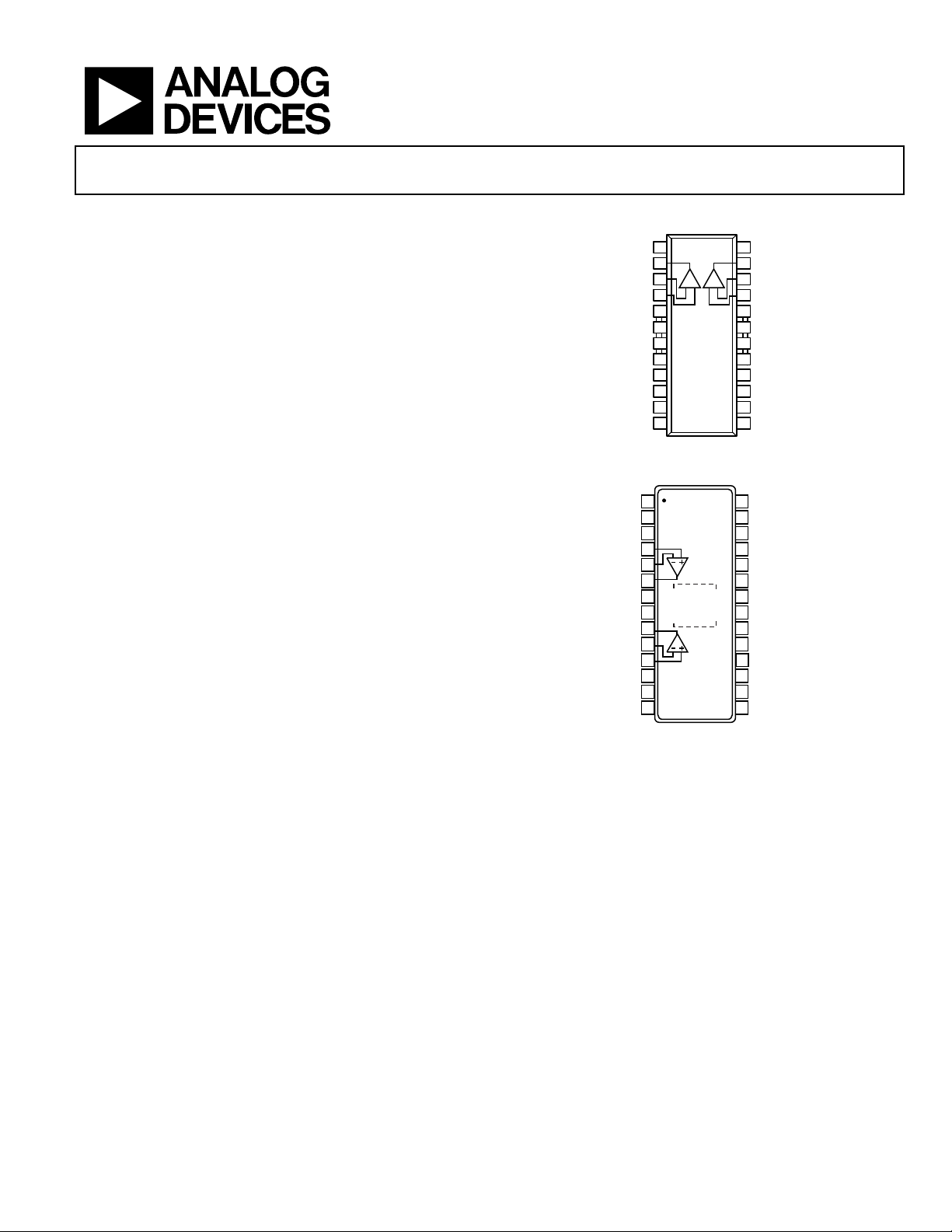
PIN CONFIGURATIONS
+V1 +V2
1
2
V
1
OUT
3
1
V
INN
4
V
1
INP
5
AGND
AGND
AGND
AGND
PWDN0
DGND
NC = NO CON NECT
AD8016
6
TOP VIEW
7
(Not to Scale)
8
9 16
10 15
11 14
–V1
12 13
NC
Figure 1. 24-Lead SOIC_W_BAT (RB-24)
1
NC NC
2
NC
3
NC
4
2
+V
IN
5
2
–V
IN
6
2
V
OUT
7
AD8016ARE
+V2
+V1
V
OUT
–V
IN
+V
IN
NC
NC
NC
NOTES
1. THE EXPOSED PADDLE IS FLOATING,
NOT ELECTRICALLY CONNECTED
INTERNALLY.
2. NC = NO CONNE CT.
8
9
1
10
1
11
1
12
13
14
TOP VIEW
(Not to Scale)
Figure 2. 28-Lead TSSOP_EP (RE-28-1)
+–
+–
24
23
22
21
20
19
18
17
28
27
26
25
24
23
22
21
20
19
18
17
16
15
V
OUT
2
V
INN
V
2
INP
AGND
AGND
AGND
AGND
PWDN1
BIAS
–V2
NC
NC
NC
NC
PWDN1
BIAS
–V2
–V1
DGND
NC
PWDN0
NC
NC
NC
2
01019-002
01019-003
GENERAL DESCRIPTION
The AD8016 high output current dual amplifier is designed for
the line drive interface in Digital Subscriber Line systems such
as ADSL, HDSL2, and proprietary xDSL systems. The drivers
are capable, in full-bias operation, of providing 24.4 dBm
output power into low resistance loads, enough to power a
20.4 dBm line, including hybrid insertion loss.
The AD8016 is available in a low cost 24-lead SOIC_W_BAT
and a 28-lead TSSOP_EP with an exposed lead frame (ePAD).
Operating from ±12 V supplies, the AD8016 requires only 1.5 W
of total power dissipation (refer to the Power Dissipation section
for details) while driving 20.4 dBm of power downstream using
Rev. C
Information furnished by Analog Devices is believed to be accurate and reliable. However, no
responsibility is assumed by Analog Devices for its use, nor for any infringements of patents or other
rights of third parties that may result from its use. Specifications subject to change without notice. No
license is granted by implication or otherwise under any patent or patent rights of Analog Devices.
Trademarks and registered trademarks are the property of their respective owners.
the xDSL hybrid in Figure 35 and Figure 36. Two digital bits
(PWDN0, PWDN1) allow the driver to be capable of full
performance, an output keep-alive state, or two intermediate
bias states. The keep-alive state biases the output transistors
enough to provide a low impedance at the amplifier outputs
for back termination.
The low power dissipation, high output current, high output
voltage swing, flexible power-down, and robust thermal
packaging enable the AD8016 to be used as the central office
(CO) terminal driver in ADSL, HDSL2, VDSL, and proprietary
xDSL systems.
One Technology Way, P.O. Box 9106, Norwood, MA 02062-9106, U.S.A.
Tel: 781.329.4700 www.analog.com
Fax: 781.461.3113 ©2012 Analog Devices, Inc. All rights reserved.
Page 2

AD8016 Data Sheet
TABLE OF CONTENTS
Features .............................................................................................. 1
Pin Configurations ........................................................................... 1
General Description ......................................................................... 1
Revision History ............................................................................... 2
Specifications ..................................................................................... 3
Logic Inputs (CMOS Compatible Logic) .................................. 4
Absolute Maximum Ratings ............................................................ 5
Maximum Power Dissipation ..................................................... 5
ESD Caution .................................................................................. 5
Pin Configurations and Function Descriptions ........................... 6
Typical Performance Characteristics ............................................. 7
Test Circuts ...................................................................................... 13
Theory of Operation ...................................................................... 14
Power Supply and Decoupling .................................................. 14
Feedback Resistor Selection ...................................................... 14
Bias Pin and PWDN Features ................................................... 14
Thermal Shutdown .................................................................... 15
Applications Information .............................................................. 16
Multitone Power Ratio (MTPR) ............................................... 16
Generating DMT ........................................................................ 17
Power Dissipation....................................................................... 17
Thermal Enhancements and PCB Layout ............................... 18
Thermal Testing .......................................................................... 18
Air Flow Test Conditions .......................................................... 18
Experimental Results ................................................................. 19
Outline Dimensions ....................................................................... 20
Ordering Guide .......................................................................... 20
REVISION HISTORY
3/12—Rev. B to Rev. C
Updated Format .................................................................. Universal
Deleted PSOP Package and Evaluation Boards (Throughout) ... 1
Added Pin Configurations and Function Descriptions Sections .. 7
Updated Outline Dimensions ....................................................... 21
Changes to Ordering Guide .......................................................... 19
11/03—Rev. A to Rev. B
Changes to Ordering Guide ............................................................ 4
Changes to TPC 21 ........................................................................... 8
Updated Outline Dimensions ..................................................19-20
Rev. C | Page 2 of 20
Page 3

Data Sheet AD8016
Bandwidth for 0.1 dB Flatness
G = +5, RF = 499 Ω, V
= 0.2 V p-p
16
38 MHz
Peaking
V
= 0.2 V p-p < 50 MHz
0.1 dB
Multitone Power Ratio1
26 kHz to 1.1 MHz, Z
= 100 Ω, P
= 20.4 dBm
–75 dBc
IMD
500 kHz, Δf = 10 kHz, RL = 100 Ω/25 Ω
−84/−80
−88/−85
dBc
Input Capacitance
2 pF
Input Common-Mode Voltage Range
−10 +10
V
SPECIFICATIONS
@ 25°C, VS = ±12 V, RL = 100 Ω, PWDN0, PWDN1 = (1, 1), T
Table 1.
Parameter Test Conditions/Comments Min Typ Max Unit
DYNAMIC PERFORMANCE
−3 dB Bandwidth G = +1, RF = 1.5 kΩ, V
G = +5, RF = 499 Ω, V
Large Signal Bandwidth V
Slew Rate V
Rise and Fall Time V
Settling Time 0.1%, V
Input Overdrive Recovery Time V
NOISE/DISTORTION PERFORMANCE
Distortion, Single-Ended V
Second Harmonic fC = 1 MHz, RL = 100 Ω/25 Ω −75/−62 −77/−64 dBc
Third Harmonic fC = 1 MHz, RL = 100 Ω/25 Ω −88/−74 −93/−76 dBc
IP3 500 kHz, RL = 100 Ω/25 Ω 42/40 43/41 dBm
Voltage Noise (RTI) f = 10 kHz 2.6 4.5 nV/√Hz
Input Current Noise f = 10 kHz 18 21 pA√Hz
INPUT CHARACTERISTICS
RTI Offset Voltage −3.0 1.0 +3.0 mV
+Input Bias Current −45 +45 μA
–Input Bias Current −75 4 +75 μA
Input Resistance 400 kΩ
= 4 V p-p 90 MHz
OUT
OUT
= 4 V p-p, G = +2 1000 V/μs
OUT
= 2 V p-p 2 ns
OUT
= 2 V p-p 23 ns
OUT
= 12.5 V p-p 350 ns
OUT
= 2 V p-p, G = +5, RF = 499 Ω
OUT
= −40°C, T
MIN
= 0.2 V p-p 380 MHz
OUT
< 0.5 V p-p 69 78 MHz
OUT
OUT
LINE
= +85°C, unless otherwise noted.
MAX
LINE
Common-Mode Rejection Ratio 58 64 dB
OUTPUT CHARACTERISTICS
Output Voltage Swing Single-ended, RL = 100 Ω −11 +11 V
Linear Output Current G = 5, RL = 10 Ω, f1 = 100 kHz, −60 dBc SFDR 400 600 mA
Short-Circuit Current 2000 mA
Capacitive Load Drive 80 pF
POWER SUPPLY
Operating Range ±3 ±13 V
Quiescent Current PWDN1, PWDN0 = (1, 1) 12.5 13.2 mA/Amp
PWDN1, PWDN0 = (1, 0) 8 10 mA/Amp
PWDN1, PWDN0 = (0, 1) 5 8 mA/Amp
PWDN1, PWDN0 = (0, 0) 4 6 mA/Amp
Recovery Time To 95% of IQ 25 μs
Shutdown Current 250 μA out of bias pin 1.5 4.0 mA/Amp
Power Supply Rejection Ratio ΔVS = ±1 V 63 75 dB
OPERATING TEMPERATURE RANGE −40 +85 °C
1
See Figure 48, R20, R21 = 0 Ω, R1 = open.
Rev. C | Page 3 of 20
Page 4

AD8016 Data Sheet
PWDN1, PWDN0 = (1, 0)
6
6.9
mA/Amp
PWDN1, PWDN0 = (0, 1)
4
5.0
mA/Amp
@ 25°C, VS = ±6 V, RL = 100 Ω, PWDN0, PWDN1 = (1, 1), T
Table 2.
Parameter Test Conditions/Comments Min Typ Max Unit
DYNAMIC PERFORMANCE
–3 dB Bandwidth G = +1, RF = 1.5 kΩ, V
G = +5, RF = 499 Ω, V
Bandwidth for 0.1 dB Flatness G = +5, RF = 499 Ω, V
Large Signal Bandwidth V
Peaking V
Slew Rate V
Rise and Fall Time V
Settling Time 0.1%, V
Input Overdrive Recovery Time V
NOISE/DISTORTION PERFORMANCE
Distortion, Single-Ended G = +5, V
Second Harmonic fC = 1 MHz, RL = 100 Ω/25 Ω −73/61 −75/−63 dBc
Third Harmonic fC = 1 MHz, RL = 100 Ω/25 Ω −80/−68 −82/−70 dBc
Multitone Power Ratio1 26 kHz to 138 kHz, Z
IMD 500 kHz, Δf = 110 kHz, RL = 100 Ω/25 Ω −87/−82 −88/−83 dBc
IP3 500 kHz 42/39 42/39 dBm
Voltage Noise (RTI) f = 10 kHz 4 5 nV/√Hz
Input Current Noise f = 10 kHz 17 20 pA√Hz
INPUT CHARACTERISTICS
RTI Offset Voltage −3.0 0.2 +3.0 mV
+Input Bias Current −25 10 +25 μA
−Input Bias Current −30 10 +30 μA
Input Resistance 400 kΩ
Input Capacitance 2 pF
Input Common-Mode Voltage Range −4 +4 V
Common-Mode Rejection Ratio 60 66 dB
OUTPUT CHARACTERISTICS
Output Voltage Swing Single-Ended, RL = 100 Ω −5 +5 V
Linear Output Current G = +5, RL = 5 Ω, f = 100 kHz, −60 dBc SFDR 300 420 mA
Short-Circuit Current 830 mA
Capacitive Load Drive RS = 10 Ω 50 pF
POWER SUPPLY
Quiescent Current PWDN1, PWDN0 = (1, 1) 8 9.7 mA/Amp
= 1 V rms 80 MHz
OUT
= 0.2 V p-p < 50 MHz 0.7 1.0 dB
OUT
= 4 V p-p, G = +2 300 V/μs
OUT
= 2 V p-p 2 ns
OUT
= 2 V p-p 39 ns
OUT
= 6.5 V p-p 350 ns
OUT
= 2 V p-p, RF = 499 Ω
OUT
= –40°C, T
MIN
= 0.2 V p-p 320 MHz
OUT
< 0.5 V p-p 70 71 MHz
OUT
= 0.2 V p-p 10 15 MHz
OUT
= 100 Ω, P
LINE
= +85°C, unless otherwise noted.
MAX
= 13 dBm −68 dBc
LINE
PWDN1, PWDN0 = (0, 0) 3 4.1 mA/Amp
Recovery Time To 95% of IQ 23 μs
Shutdown Current 250 μA out of bias pin 1.0 2.0 mA/Amp
Power Supply Rejection Ratio ΔVS = ±1 V 63 80 dB
OPERATING TEMPERATURE RANGE −40 +85 °C
1
See Figure 48, R20, R21 = 0 Ω, R1 = open.
LOGIC INPUTS (CMOS COMPATIBLE LOGIC)
PWDN0, PWDN1, VCC = ±12 V or ±6 V; full temperature range.
Table 3.
Parameter Min Typ Max Unit
Logic 1 Voltage 2.2 VCC V
Logic 0 Voltage 0 0.8 V
Rev. C | Page 4 of 20
Page 5
Data Sheet AD8016
A
ABSOLUTE MAXIMUM RATINGS
Table 4.
Parameter Rating
Supply Voltage 26.4 V
Internal Power Dissipation
SOIC_W_BAT Package1 1.4 W
TSSOP_EP Package2 1.4 W
Input Voltage (Common-Mode) ±VS
Differential Input Voltage ±VS
Output Short-Circuit Duration Observe power derating
Storage Temperature Range −65°C to +125°C
Operating Temperature Range −40°C to +85°C
Lead Temperature Range (Soldering 10 sec) 300°C
1
Specification is for device on a 4-layer board with 10 inches2 of 1 oz copper
at 85°C 24-lead SOIC_W_BAT package: θ
2 Specification is for device on a 4-layer board with 9 inches2 of 1 oz copper at
85°C 28-lead (TSSOP_EP) package: θJA = 29°C/W.
= 28°C/W.
JA
curves
Stresses above those listed under Absolute Maximum Ratings
may cause permanent damage to the device. This is a stress
rating only; functional operation of the device at these or any
other conditions above those indicated in the operational
section of this specification is not implied. Exposure to absolute
maximum rating conditions for extended periods may affect
device reliability.
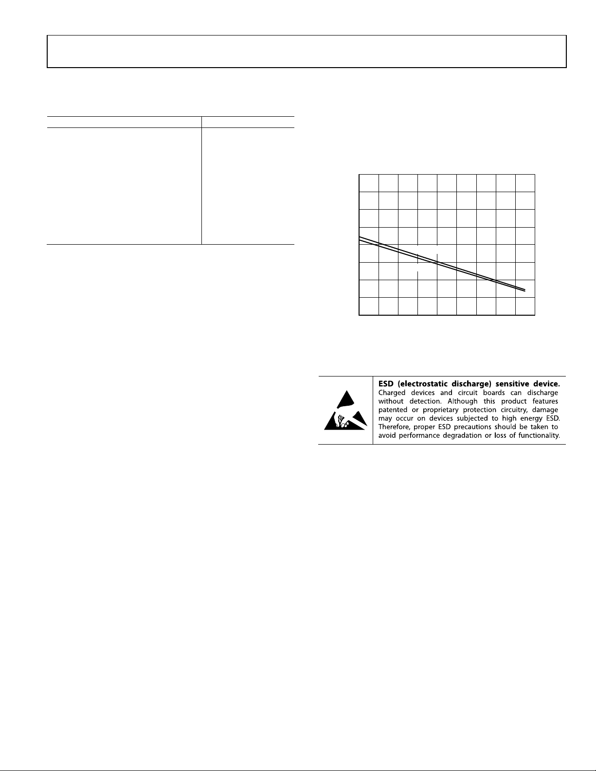
MAXIMUM POWER DISSIPATION
The maximum power that can be safely dissipated by the
AD8016 is limited by the associated rise in junction temper-
ature. The maximum safe junction temperature for a plastic
encapsulated device is determined by the glass transition
temperature of the plastic, approximately 150°C. Temporarily
exceeding this limit may cause a shift in parametric performance due to a change in the stresses exerted on the die by
the package.
The output stage of the AD8016 is designed for maximum load
current capability. As a result, shorting the output to common
can cause the AD8016 to source or sink 2000 mA. To ensure
proper operation, it is necessary to observe the maximum
power derating curves. Direct connection of the output to
either power supply rail can destroy the device.
8
7
6
TION (W)
5
4
3
2
MAXIMUM POWER DISSIP
1
0
010
Figure 3. Maximum Power Dissipation vs. Temperature for AD8016 for
SOIC_W_BAT
TSSOP-EP
20 30 40 50 60 70 80 90
AMBIENT TEMPERATURE (°C)
T
= 125 °C
J
01019-005
ESD CAUTION
Rev. C | Page 5 of 20
Page 6
AD8016 Data Sheet
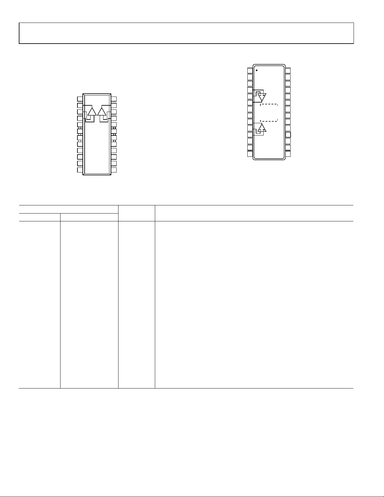
PIN CONFIGURATIONS AND FUNCTION DESCRIPTIONS
+V1 +V2
1
2
V
1
OUT
3
1
V
INN
4
V
1
INP
5
AGND
6
AGND
7
AGND
8
AGND
9 16
PWDN0
10 15
DGND
11 14
–V1
12 13
NC
NC = NO CON NECT
+–
+–
AD8016
TOP VIEW
(Not to Scale)
24
23
22
21
20
19
18
17
V
OUT
2
V
INN
V
2
INP
AGND
AGND
AGND
AGND
PWDN1
BIAS
–V2
NC
1
NC NC
2
NC
3
NC
4
+V
2
IN
5
–V
2
IN
6
V
2
2
01019-002
OUT
7
AD8016ARE
+V2
+V1
V
OUT
–V
IN
+V
IN
NC
NC
NC
NOTES
1. THE EXPOSED PADDLE IS FLOATING,
NOT ELECTRICALLY CONNECTED
INTERNALLY.
2. NC = NO CONNE CT.
8
9
1
10
1
11
1
12
13
14
TOP VIEW
(Not to Scale)
28
27
26
25
24
23
22
21
20
19
18
17
16
15
NC
NC
NC
PWDN1
BIAS
–V2
–V1
DGND
NC
PWDN0
NC
NC
NC
01019-003
Figure 4. 24-Lead SOIC_W_BAT (RB-24) Figure 5. 28-Lead TSSOP_EP (RE-28-1)
Table 5. Pin Function Descriptions
Pin No.
Mnemonic Description SOIC_W_BAT TSSOP_EP
1 8 +V1 Positive Power Supply, Amp 1.
2 9 V
3 V
4 V
1 Output Signal, Amp 1.
OUT
1 Negative Input Signal, Amp 1.
INN
1 Positive Input Signal, Amp1.
INP
5 to 8, 17 to 20 AGND Analog Ground.
9 18 PWDN0 Power-Down Input 0.
10 20 DGND Digital Ground.
11 21 −V1 Negative Power Supply, Amp1.
12, 13
1 to 3, 12 to 17, 19,
NC This pin is not connected internally (see Figure 4 and Figure 5).
25 to 28
14 22 −V2 −V Power Supply, Amp 2.
15 23 BIAS Quiescent Current Adjust.
16 24 PWDN1 Power-Down Input 1.
21 V
22 V
23 6 V
2 Positive Input Signal, Amp 2.
INP
2 Negative Input Signal, Amp 2.
INN
2 Output Signal, Amp 2.
OUT
24 7 +V2 Positive Power Supply, Amp 2.
4 +VIN2 Positive Input Signal, Amp 2.
5 −VIN2 Negative Input Signal, Amp 2.
10 −VIN1 Negative Input Signal, Amp 1.
11 +VIN1 Positive Input Signal, Amp 1.
EP EPAD Exposed Pad. The exposed paddle is floating, not electrically connected internally.
Rev. C | Page 6 of 20
Page 7

Data Sheet AD8016
10dB/DIV
V
OUT
= 100mV
VIN = 20mV
VOLTS
TIME (100ns/DIV)
01019-008
V
OUT
= 5V
VIN = 800mV
TIME (100ns/DIV)
VOLTS
01019-009
V
OUT
= 100mV
V
IN
= 20mV
VOLTS
TIME (100ns/DIV)
01019-010
VOLTS
TIME (100ns/DIV)
V
OUT
= 4V
V
IN
= 800mV
01019-011
(1,0)
(0,1)
FREQUENCY (MHz)
–30
100.01
DISTORTION (dBc)
10.1
–110
–100
–90
–80
–70
–60
–50
–40
20
RF = 499Ω
G = +10
V
OUT
= 4V p-p
(0,0)
PWDN1, PW DN0 = ( 1,1)
01019-012
TYPICAL PERFORMANCE CHARACTERISTICS
–75dBc
549.3
550.3 551.3 552.3 553.3 554.3 555.3 556.3 557.3 558.3 559.3
FREQUENCY ( kHz )
01019-004
Figure 6. Multitone Power Ratio; VS = ±12 V, 20.4 dBm Output Power into
100 Ω, Downstream
Figure 9. 100 mV Step Response; G = +5, V
= ±12 V, RL = 25 Ω, Single-Ended
S
Figure 7. 100 mV Step Response; G = +5, VS = ±6 V, RL = 25 Ω, Single-Ended
Figure 8. 4 V Step Response; G = +5, V
= ±6 V, RL = 25 Ω, Single-Ended
S
Rev. C | Page 7 of 20
Figure 10. 4 V Step Response; G = +5, V
= ±12 V, RL = 25 Ω, Single-Ended
S
Figure 11. Distortion vs. Frequency; Second Harmonic, VS = ±12 V, RL = 50 Ω,
Differential
Page 8

AD8016 Data Sheet
–
–
–
–
–
–
30
RF = 499Ω
G = +10
V
= 4V p-p
–40
OUT
–50
–60
–70
–80
DISTORTION (dBc)
–90
–100
–110
FREQUENCY (MHz)
PWDN1, PWDN0 = (1,1)
Figure 12. Distortion vs. Frequency; Second Harmonic, V
30
RF = 499Ω
G = +5
–35
–40
–45
–50
DISTORTION (d Bc)
–55
–60
–65
–70
–75
–80
0 100
(0,0)
(0,1)
300400500600700800
200
PEAK OUTPUT CURRENT (mA)
(1,0)
PWDN1, PW DN0 = (1,1)
(0,0)
(0,1)
100.01 10.1 20
= ±6 V, RL = 50 Ω
S
Figure 13. Distortion vs. Peak Output Current; Second Harmonic, V
= 10 Ω, f = 100 kHz, Single-Ended
R
L
30
RF = 499Ω
G = +10
V
OUT
= 4V p-p
FREQUENCY (MHz)
DISTORTION (dBc)
–100
–110
–40
–50
–60
–70
–80
–90
Figure 14. Distortion vs. Frequency; Third Harmonic, V
(0,0)
(0,1)
(1,0)
PWDN1, P WDN0 = (1, 1)
100.01 10. 1 20
= ±12 V, RL = 50 Ω,
S
Differential
(1,0)
S
01019-013
01019-014
= ±12 V,
01019-015
30
RF = 499Ω
G = +10
= 4V p-p
V
–40
OUT
–50
–60
–70
–80
DISTORTION (dBc)
–90
–100
–110
FREQUENCY (MHz)
Figure 15. Distortion vs. Frequency; Third Harmonic, V
(0,0)
(0,1)
PWDN1, PWDN0 = (1,1)
= ±6 V, RL = 50 Ω,
S
(1,0)
100.01 10.1 20
Differential
30
RF = 499Ω
G = +5
–40
–50
–60
–70
DISTOR TION (d Bc)
–80
–90
0 100
(0,0)
(0,1)
300 400 500 600 700
200
PEAK OUTP UT CURRENT (mA)
(1,0)
PWDN1,
PWDN0 = (1, 1)
Figure 16. Distortion vs. Peak Output Current, Third Harmonic; V
R
= 10 Ω, G = +5, f = 100 kHz, Single-Ended
L
30
RF = 499Ω
G = +5
–35
–40
–45
–50
–55
–60
DISTORTION (dBc)
–65
–70
–75
–80
0100
(0,0)
(0,1)
(1,0)
PWDN1, PWDN0 = (1,1)
200
PEAK OUTP UT CURRENT (mA)
300 400 500 600
Figure 17. Distortion vs. Peak Output Current; Second Harmonic, V
= 5 Ω, f = 100 kHz, Single-Ended
R
L
= ±12 V,
S
= ±6 V,
S
01019-016
01019-017
01019-018
Rev. C | Page 8 of 20
Page 9

Data Sheet AD8016
–
–
–
–
–
30
30
–40
–50
–60
–70
DISTO RTION ( dBc)
–80
–90
–100
05
15 20 25 30 35 40
10
DIFFERENTIAL OUTPUT (V p-p)
(0,0)
(0,1)
(1,0)
PWDN1, P WDN0 = (1, 1)
Figure 18. Distortion vs. Output Voltage; Second Harmonic, V
G = +10, f = 1 MHz, R
30
–40
–50
–60
–70
DISTORTION (dBc)
–80
–90
05
DIFFERENTIAL OUTPUT (V p-p)
= 50 Ω, Differential
L
(0,0)
10
(0,1)
(1,0)
PWDN1, PWDN0 = (1,1)
15 20
Figure 19. Distortion vs. Output Voltage; Second Harmonic, V
30
–35
–40
–45
–50
–55
–60
DISTORTION (dBc)
–65
–70
–75
–80
0100
G = +10, f = 1 MHz, R
(0,0)
200
PEAK OUTP UT CURRENT (mA)
= 50 Ω, Differential
L
(0,1)
(1,0)
PWDN1, PWDN0 = (1,1)
300 400 500 600
Figure 20. Distortion vs. Peak Output Current; Third Harmonic, V
G = +5, R
= 5 Ω, f = 100 kHz, Single-Ended
L
= ±12 V,
S
= ±6 V,
S
= ±6 V,
S
–40
–50
–60
–70
DISTORT ION (d Bc)
–80
–90
–100
01019-020
05
10
Figure 21. Distortion vs. Output Voltage; Third Harmonic, V
G = +10, f = 1 MHz, R
30
–40
–50
–60
–70
DISTORTION (d Bc)
–80
–90
01019-021
05
Figure 22. Distortion vs. Output Voltage, Third Harmonic, V
f = 1 MHz, R
3
0
–3
–6
–9
–12
–15
–18
–21
VIN = 40mV p-p
–24
G = +5
NORMALIZED FREQUENCY RESPONSE (dB)
R
= 100Ω
L
–27
01019-022
1500100
Figure 23. Frequency Response; V
(0,0)
(0,1)
(1,0)
PWDN1, PW DN0 = (1,1)
15 20 25 30 35 40
DIFFERENTIAL OUTPUT (V p-p)
= 50 Ω, Differential
L
(0,0)
(0,1)
PWDN1, PW DN0 = (1,1)
DIFFERENTIAL OUTPUT (V p-p)
10
= 50 Ω, Differential
L
10
FREQUENCY (MHz)
= ±12 V, @ PWDN1, PWDN0 Codes
S
15 20
= ±12 V,
S
(1,0)
= ±6 V, G = +10,
S
(1,1)
(1,0)
(0,1)
(0,0)
01019-023
01019-024
01019-025
Rev. C | Page 9 of 20
Page 10

AD8016 Data Sheet
FREQUENCY (MHz)
1
OUTPUT VOLTAGE (dBV)
–16
–19
–13
–10
–7
–4
–1
2
5
8
11
500100
10
G = +5
R
L
= 100Ω
R
F
= 499Ω
01019-026
FREQUENCY (MHz)
20
0.03
CMRR (dB)
10
0
–10
–20
–30
–40
–50
–60
–70
–80
VIN= 2V rms
R
F
= 602
Ω
(1,1)
(1,0)
(0,1)
(0,0)
500100
100.1
1
01019-027
500100
FREQUENCY (MHz)
10
1
3
0
–3
–6
–9
–12
–15
–18
–21
–24
6
NORMALIZED FREQUENCY RE S P ONSE (dB)
(1,1)
(0,1)
(1,0)
(0,0)
V
IN
= 40mV p-p
G = +5
RL = 100Ω
01019-028
500100
10
FREQUENCY (MHz)
1
OUTPUT VOLTAGE (dBV)
–16
–19
–13
–10
–7
–4
–1
2
5
8
11
G = +5
R
L
= 100Ω
R
F
= 499Ω
01019-029
500100
100.10.01
1
FREQUENCY (MHz)
–10
PSRR (dB)
–20
–30
–40
–50
–60
–70
–80
–90
+PSRR
–PSRR
RF = 499Ω
01019-030
0
FREQUENCY (MHz)
10
INPUT VOLTAGE NOISE (nV/ Hz)
100
80
60
40
20
10M10k1k100
10
20
30
40
50
60
70
80
90
+ INPUT CURRENT NOISE (pA/ Hz)
0
120
140
160
180
100k 1M
+I
NOISE
V
IN NOISE
01019-031
Figure 24. Output Voltage vs. Frequency; VS = ±12 V
Figure 25. CMRR vs. Frequency; VS = ±12 V @ PWDN1, PWDN0 Codes
Figure 27. Output Voltage vs. Frequency; VS = ±6 V
Figure 28. PSRR vs. Frequency; VS = ±12 V
Figure 26. Frequency Response; V
= ±6 V, @ PWDN1, PWDN0 Codes
S
Figure 29. Noise vs. Frequency
Rev. C | Page 10 of 20
Page 11

Data Sheet AD8016
+2mV
(–0.1%)
–2mV
(–0.1%)
0
G = +2
R
F
= 1kΩ
V
OUT
= 2V
STEP
R
L
= 100
Ω
OUTPUT VOLTAGE ERROR (2mV/ DIV (0.1%/DIV))
–5 0 5 10 15 20 25 30 35 40 45
TIME (ns)
V
IN
V
OUT
V
OUT
– V
IN
01019-032
FREQUENCY (MHz)
–30
0.03
CROSSTAL K ( dB)
0.1 1 10 100 500
–40
–50
–60
–70
–80
–90
–20
V
OUT
= 2V p-p
R
F
= 499Ω
G = +5
R
L
= 100Ω
01019-033
1010.10.010.0010.0001 10k1k100
FREQUENCY (MHz)
1M
TRANSIMPE DANCE ( k
Ω
)
100k
10k
1k
100
10
1
0.1
0.01
0.001
0
40
80
120
160
200
240
280
320
360
PHASE (Degrees)
TRANSIMPEDANCE
PHASE
01019-034
–5 0 5
10 15 20
25 30 35 40 45
OUTPUT VOLTAGE ERROR (2mV/ DIV (0.1%/DIV))
TIME (ns)
+2mV
(–0.1%)
–2mV
(–0.1%)
0
V
OUT
V
IN
V
OUT
– V
IN
G = +2
R
F
= 1kΩ
V
OUT
= 2V
STEP
R
L
= 100
Ω
01019-035
1010.1
500
100
FREQUENCY (MHz)
1000
0.03
OUTPUT IMPEDANCE (
Ω
)
100
10
1
0.1
0.01
(0,0)
(0,1)
(1,1)
(1,0)
01019-036
VIN = 2V/DIV
V
OUT
= 5V/DIV
V
IN
V
OUT
–100 100 200 300 400 500 600 700 800 9000
TIME (ns)
0V
0V
01019-037
Figure 30. Settling Time 0.1%; VS = ±12 V
Figure 33. Settling Time 0.1%; VS = ±6 V
Figure 31. Output Crosstalk vs. Frequency
Figure 32. Open-Loop Transimpedance and Phase vs. Frequency
Figure 34. Output Impedance vs. Frequency @ PWDN1, PWDN0 Codes
Rev. C | Page 11 of 20
Figure 35. Positive Overdrive Recovery; V
= ±12 V, G = +5, RL = 100 Ω
S
Page 12

AD8016 Data Sheet
–100 100 200 300 400 500 600 700 800 9000
TIME (ns)
V
IN
V
OUT
0V
0V
VIN = 2V/DIV
V
OUT
= 5V/DIV
01019-038
I
BIAS
(µA)
25
0
I
Q
(mA)
20
15
10
5
0
50 100 150 200
(0,1)
(0,0)
(1,0)
PWDN1, PW DN0 = ( 1,1)
01019-039
I
BIAS
(µA)
18
0
I
Q
(mA)
16
14
12
10
8
50 100 150 200
6
4
2
0
(1,0)
(0,1)
(0,0)
PWDN1, PW DN0 = ( 1,1)
01019-040
R
LOAD
(
Ω
)
OUTPUT SWING (V)
12
8
10
100 1k 10k
4
0
–4
–8
–12
+V
OUT
, V
S
= ±12V
+V
OUT
, VS = ±6V
–V
OUT
, VS = ±12V
–V
OUT
, VS = ±6V
01019-041
Figure 36. Negative Overdrive Recovery; V
Figure 37. I
vs. I
Q
= ±12 V, G = +5, RL = 100 Ω
S
Current; VS = ±12 V
BIAS
Figure 38. I
Q
vs. I
BIAS
Current; VS = ±6 V
Figure 39. Output Voltage vs. R
LOAD
Rev. C | Page 12 of 20
Page 13

Data Sheet AD8016
0.1µF
0.1µF
10µF
10µF
49.9
Ω
124
Ω
499
Ω
R
L
V
OUT
+V
S
–V
S
+
+
V
IN
01019-006
499Ω
49.9Ω
+V
IN
R
L
499Ω
111Ω
49.9Ω
–V
IN
+V
O
–V
O
+V
S
–V
S
10µF
+
0.1µF
0.1µF
10µF
+
01019-007
TEST CIRCUTS
Figure 40. Single-Ended Test Circuit; G = +5
Figure 41. Differential Test Circuit; G = +10
Rev. C | Page 13 of 20
Page 14

AD8016 Data Sheet
FIN
Z
Z
IN
OUT
RRGST
S
T
G
V
V
+×+×=)(
)(
G
F
R
R
G += 1
Ω≈= 25
1
m
IN
g
R
+10
1000
111
T
Z
R
IN
I
IN
+
+
–
R
F
V
OUT
R
N
R
G
V
IN
01019-042
THEORY OF OPERATION
The AD8016 is a current feedback amplifier with high
(500 mA) output current capability. With a current feedback
amplifier, the current into the inverting input is the feedback
signal and the open-loop behavior is that of a transimpedance,
dV
/dIIN or TZ. The open-loop transimpedance is analogous
OUT
to the open-loop voltage gain of a voltage feedback amplifier.
Figure 42 shows a simplified model of a current feedback amplifie r. Because R
gain is just T
is proportional to 1/gm, the equivalent voltage
IN
× gm, where gm is the transconductance of the
Z
input stage. Basic analysis of the follower with gain circuit yields
where:
Recognizing that G × R
<< RF for low gains, the familiar result
IN
of constant bandwidth with gain for current feedback amplifiers
is evident, the 3 dB point being set when |T
| = RF. Of course,
Z
for a real amplifier there are additional poles that contribute
excess phase and there is a value for R
below which the ampli-
F
fier is unstable. Tolerance for peaking and desired flatness
determines the optimum R
in each application.
F
POWER SUPPLY AND DECOUPLING
The AD8016 should be powered with a good quality (that is,
low noise) dual supply of ±12 V for the best distortion and
multitone power ratio (MTPR) performance. Careful attention
must be paid to decoupling the power supply pins. A 10 μF
capacitor located in near proximity to the AD8016 is required
to provide good decoupling for lower frequency signals. In
addition, 0.1 μF decoupling capacitors should be located as
close to each of the four power supply pins as is physically
possible. All ground pins should be connected to a common
low impedance ground plane.
FEEDBACK RESISTOR SELECTION
In current feedback amplifiers, selection of feedback and gain
resistors has an impact on the MTPR performance, bandwidth,
and gain flatness. Tak e care in selecting these resistors so that
optimum performance is achieved. Tabl e 6 below shows the
recommended resistor values for use in a variety of gain
settings. These values are suggested as a good starting point
when designing for any application.
Table 6. Resistor Selection Guide
Gain RF (Ω) RG (Ω)
+1 1000 ∞
−1 500 500
+2 650 650
+5 750 187
Figure 42. Simplified Block Diagram
The AD8016 is the first current feedback amplifier capable of
delivering 400 mA of output current while swinging to within
2 V of either power supply rail. This enables full CO ADSL
performance on only 12 V rails, an immediate 20% power
saving. The AD8016 is also unique in that it has a power
management system included on-chip. It features four user
programmable power levels (all of which provide a low output
impedance of the driver), as well as the provision for complete
shutdown (high impedance state). Also featured is a thermal
shutdown with alarm signal.
Rev. C | Page 14 of 20
BIAS PIN AND PWDN FEATURES
The AD8016 is designed to cover both central office (CO)
and customer premise equipment (CPE) ends of an xDSL
application. It offers full versatility in setting quiescent bias
levels for the particular application from full on to reduced
bias (in three steps) to full off (via BIAS pin). This versatility
gives the modem designer the flexibility to maximize efficiency
while maintaining reasonable levels of MTPR performance.
Optimizing driver efficiency while delivering the required DMT
power is accomplished with the AD8016 through the use of onchip power management features. Two digitally programmable
logic pins, PWDN1 and PWDN0, may be used to select four
different bias levels: 100%, 60%, 40%, and 25% of full quiescent
power (see Table 7).
Table 7. PWDN Code Selection Guide
PWDN1
Code
1 1 100% (full on)
1 0 60%
0 1 40%
0 0 25% (low Z
X X Full off (high Z
PWDN0
Code Quiescent Bias Level
but not off)
OUT
via 250 μA pulled out of
OUT
BIAS pin)
Page 15

Data Sheet AD8016
*
V
The bias level can be controlled with TTL logic levels (high = 1)
applied to the PWDN1 and PWDN0 pins alone or in combination with the BIAS control pin. The DGND or digital ground
pin is the logic ground reference for the PWDN1 and PWDN0
pins. In typical ADSL applications where ±12 V or ±6 V
supplies (also single supplies) are used, the DGND pin is
connected to analog ground.
The BIAS control pin by itself is a means to continuously adjust
the AD8016 internal biasing and, thus, quiescent current I
Q
. By
pulling out a current of 0 μA (or open) to approximately200 μA,
the quiescent current can be adjusted from 100% (full on) to a
full off condition. The full off condition yields a high output
impedance. Because of an on-chip resistor variation of up to
±20%, the actual amount of current required to fully shut down
the AD8016 can vary. To institute a full chip shutdown, a pulldown current of 250 μA is recommended. See Figure 43 for the
logic drive circuit for complete amplifier shutdown. Figure 37
and Figure 38 show the relationship between current pulled out
of the BIAS pin (I
shutdown I
is less than 1 mA total. Alternatively, an external
Q
) and the supply current (IQ). A typical
BIAS
pull-down resistor to ground or a current sink attached to the
BIAS pin can be used to set I
to lower levels (see Figure 44).
Q
The BIAS pin may be used in combination with the PWDN1
and PWDN0 pins; however, diminished MTPR performance
may result when I
is lowered too much. Current pulled away
Q
from the BIAS pin shunts away a portion of the internal bias
current. Setting PWDN1 or PWDN0 to Logic 0 also shunts
away a portion of the internal bias current. The reduction of
quiescent bias levels due to the use of PWDN1 and PWDN0 is
consistent with the percentages established in Table 7. When
PWDN0 alone is set to Logic 0, and no other means of reducing
the internal bias currents is used, full-rate ADSL signals may be
driven while maintaining reasonable levels of MTPR.
3.3V LOGI C
R2
50kΩ
R1*
2N3904
BIAS
THERMAL SHUTDOWN
The AD8016 ARB is designed to incorporate shutdown
protection against accidental thermal overload. In the event
of thermal overload, the AD8016 was designed to shut down
at a junction temperature of 165°C and return to normal
operation at a junction temperature 140°C. The AD8016
continues to operate, cycling on and off, as long as the thermal
overload condition remains. The frequency of the protection
cycle depends on the ambient environment, severity of the
thermal overload condition, the power being dissipated, and
the thermal mass of the PCB beneath the AD8016. When the
AD8016 begins to cycle due to thermal stress, the internal
shutdown circuitry draws current out of the node connected
in common with the BIAS pin, while the voltage at the BIAS
pin goes to the negative rail. When the junction temperature
returns to 140°C, current is no longer drawn from this node,
and the BIAS pin voltage returns to the positive rail. Under
these circumstances, the BIAS pin can be used to trip an alarm
indicating the presence of a thermal overload condition.
Figure 44 also shows three circuits for converting this signal to
a standard logic level.
V
CC
AD8016
BIAS
200µA
PWDN0
10kΩ
10kΩ
SHUTDOWN
BIAS
PWDN1
V
CC
5V
ALARM
1/4 HCF 40109B
SGS–THOMSON
Figure 44. Shutdown and Alarm Circuit
V
EE
OR
V = VCC–0.2V
BIAS
1MΩ
BIAS
100kΩ
OR
0µA – 200µA
5V
10kΩ
ALARM
MIN β 350
01019-044
R1 = 47kΩ FOR ±12VS OR +12VS,
R1 = 22kΩ FOR ±6
.
S
01019-043
Figure 43. Logic Drive of BIAS Pin for Complete Amplifier Shutdown
Rev. C | Page 15 of 20
Page 16

AD8016 Data Sheet
( )
2
2
2 N
Z
Z×≡
′
4
1.0
3
2
1.2 1.4 2.0
1
0
–1
1.6 1.8
–2
1.1 1.3 1.5 1.7 1.9
DOWNSTRE AM TURNS RATIO
DYNAMIC HEADROOM (dB)
VS = ±12V
PWDN1, PW DN0 = ( 1,1)
VS = ±11.4V
PWDN1, PW DN0 = ( 1,1)
VS = ±12V
PWDN1, PW DN0 = ( 1,0)
VS = ±11.4V
PWDN1, PW DN0 = ( 1,0)
01019-045
APPLICATIONS INFORMATION
The AD8016 dual amplifier forms an integrated single-channel
ADSL line driver. The AD8016 may be applied in driving modulated signals including discrete multitone (DMT) in either
direction; upstream from CPE to the CO and downstream
from CO to CPE. The most significant thermal management
challenge lies in driving downstream information from CO sites
to the CPE. Driving xDSL information downstream suggests
the need to locate many xDSL modems in a single CO site. The
implication is that several modems will be placed onto a single
printed circuit board residing in a card cage located in a variety
of ambient conditions. Environmental conditioners such as fans
or air conditioning may or may not be available, depending on
the density of modems and the facilities contained at the CO
site. To achieve long-term reliability and consistent modem
performance, designers of CO solutions must consider the wide
array of ambient conditions that exist within various CO sites.
MULTITONE POWER RATIO (MTPR)
ADSL systems rely on discrete multitone modulation to carry
digital data over phone lines. DMT modulation appears in the
frequency domain as power contained in several individual
frequency subbands, sometimes referred to as tones or bins,
each of which is uniformly separated in frequency. (See Figure 6
for an example of downstream DMT signals used in evaluating
MTPR performance.) A uniquely encoded, quadrature amplitude modulation (QAM) signal occurs at the center frequency
of each subband or tone. Difficulties arise when decoding these
subbands if a QAM signal from one subband is corrupted by the
QAM signal(s) from other subbands, regardless of whether the
corruption comes from an adjacent subband or harmonics of
other subbands. Conventional methods of expressing the output
signal integrity of line drivers, such as spurious-free dynamic
range (SFDR), single-tone harmonic distortion or THD, twotone intermodulation distortion (IMD), and third-order intercept (IP3) become significantly less meaningful when amplifiers
are required to drive DMT and other heavily modulated
waveforms. A typical xDSL downstream DMT signal may
contain as many as 256 carriers (subbands or tones) of QAM
signals. MTPR is the relative difference between the measured
power in a typical subband (at one tone or carrier) vs. the power
at another subband specifically selected to contain no QAM
data. In other words, a selected subband (or tone) remains
open or void of intentional power (without a QAM signal),
yielding an empty frequency bin. MTPR, sometimes referred
to as the empty bin test, is typically expressed in dBc, similar
to expressing the relative difference between single-tone
fundamentals and second or third harmonic distortion
components.
See Figure 6 for a sample of the ADSL downstream spectrum
showing MTPR results while driving 20.4 dBm of power onto
a 100 Ω line. Measurements of MTPR are typically made at
the output (line side) of ADSL hybrid circuits. MTPR can be
affected by the components contained in the hybrid circuit,
including the quality of the capacitor dielectrics, voltage ratings,
and the turns ratio of the selected transformers. Other components aside, an ADSL driver hybrid containing the AD8016 can
be optimized for the best MTPR performance by selecting the
turns ratio of the transformers. The voltage and current demands
from the differential driver changes, depending on the transformer turns ratio. The point on the curve indicating maximum
dynamic headroom is achieved when the differential driver
delivers both the maximum voltage and current while maintaining
the lowest possible distortion. Below this point, the driver has
reserve current-driving capability and experiences voltage
clipping. Above this point, the amplifier runs out of current
drive capability before the maximum voltage drive capability
is reached. Because a transformer reflects the secondary load
impedance back to the primary side by the square of the turns
ratio, varying the turns ratio changes the load across the
differential driver. The following equation may be used to
calculate the load impedance across the output of the differential driver, reflected by the transformers, from the line side of
the xDSL driver hybrid.
where:
Z' is the primary side impedance as seen by the differential
driver.
Z
is the line impedance.
2
N is the transformer turns ratio.
Figure 45 shows the dynamic headroom in each subband of a
downstream DMT waveform vs. turns ratio running at 100%
and 60% of the quiescent power while maintaining −65 dBc
of MTPR at V
Rev. C | Page 16 of 20
= ±12 V.
S
Figure 45. Dynamic Headroom vs. XFMR Turns Ratio, V
= ±12 V
S
Page 17

Data Sheet AD8016
01
0
0.120
N/A
L
OUT
OUT
SSQ
D
R
V
VVVIP )(42 −×+××=
−+××=
L
OUT
L
S
OUT
SQ
D
R
V
R
VV
VIP
2
4
22
π
OUTPUT P OWER (mW)
2.5
0
POWER DISSIPATION
2.0
1.5
100 200 300
1.0
0.5
0
MEASURED
SINE
MEASURED
DMT
CALCULATED
01019-046
Once an optimum turns ratio is determined, the amplifier has
an MTPR performance for each setting of the power-down
pins. Ta ble 8 demonstrates the effects of reducing the total
power dissipated by using the PWDN pins on MTPR performance when driving 20.4 dBm downstream onto the line with
a transformer turns ratio of 1:1.4.
Table 8. Dynamic Power Dissipation of Downstream
Transmission
PWDN1 PWDN0 PD (W) MTPR
1 1 1.454 −78 dBc
1 0 1.262 −75.3 dBc
0 1 1.142 −57.2 dBc
1
This mode is quiescent power dissipation.
GENERATING DMT
At this time, DMT modulated waveforms are not typically
menu selectable items contained within arbitrary waveform
generators. Even using AWG software to generate DMT signals,
AWGs that are available today may not deliver DMT signals
sufficient in performance with regard to MTPR due to limitations in the DAC and output drivers used by AWG manufacturers.
Similar to evaluating single-tone distortion performance of an
amplifier, MTPR evaluation requires a DMT signal generator
capable of delivering MTPR performance better than that of
the driver under evaluation.
The situation is more complicated with a complex modulated
signal. In the case of a DMT signal, taking the equivalent sine
wave power overestimates the power dissipation by ~23%. For
example:
P
= 23.4 dBm = 220 mW
OUT
V
@ 50 Ω = 3.31 V rms
OUT
= 2.354 V
V
OUT
at each amplifier output, which yields a P
of 1.81 W.
D
Through measurement, a DMT signal of 23.4 dBm requires
1.47 W of power to be dissipated by the AD8016. Figure 46
shows the results of calculation and actual measurements
detailing the relationship between the power dissipated by
the AD8016 vs. the total output power delivered to the back
termination resistors and the load combined. A 1:2 transformer
turns ratio was used in the calculations and measurements.
POWER DISSIPATION
To properly size the heat sinking area for the user’s application,
it is important to consider the total power dissipation of the
AD8016. The dc power dissipation for V
V
), or 2 × I
EE
× V
Q
.
S
For the AD8016 powered on +12 V and −12 V supplies (±V
the number is 0.6 W. In a differential driver circuit (Figure 41),
one can use symmetry to simplify the computation for a dc
input signal.
where:
V
is the peak output voltage of an amplifier.
OUT
This formula is slightly pessimistic due to the fact that some of
the quiescent supply current is commutated during sourcing or
sinking current into the load. For a sine wave source, integration over a half cycle yields
= 0 V is IQ (VCC −
IN
),
S
Rev. C | Page 17 of 20
Figure 46. Power Dissipation vs. Output Power (Including Back
Terminations), See Figure 9 for Test Circuit
Page 18

AD8016 Data Sheet
THERMAL ENHANCEMENTS AND PCB LAYOUT
There are several ways to enhance the thermal capacity of the
CO solution. Additional thermal capacity can be created using
enhanced PCB layout techniques such as interlacing (sometimes referred to as stitching or interconnection) of the layers
immediately beneath the line driver. This technique serves to
increase the thermal mass or capacity of the PCB immediately
beneath the driver. The AD8016 in a TSSOP_EP (ARE model)
package can be designed to operate in the CO solution using
prudent measures to manage the power dissipation through
careful PCB design. The ARE package is available for use in
designing the highest density CO solutions. Maximum heat
transfer to the PCB can be accomplished using the ARE
package when the thermal slug is soldered to an exposed
copper pad directly beneath the AD8016. Optimum thermal
performance can be achieved in the ARE package only when
the back of the package is soldered to a PCB designed for
maximum thermal capacity (see Figure 48). Thermal experiments with the ARE package were conducted without soldering
the heat slug to the PCB. Heat transfer was through physical
contact only. The following offers some insight into the AD8016
power dissipation and relative junction temperature, as well as
the effects of PCB size and composition on the junction-to-air
thermal resistance or θ
.
JA
THERMAL TESTING
A wind tunnel study was conducted to determine the relationship between thermal capacity (that is, printed circuit board
copper area), air flow, and junction temperature. Junction-toambient thermal resistance, θ
AD8016 ARE and AD8016 ARB packages. The AD8016 was
operated in a noninverting differential driver configuration,
typical of an xDSL application yet isolated from any other
modem components. Testing was conducted using a 1 oz.
copper board in an ambient temperature of ~24°C over air
flows of 200, 150, 100, and 50 linear feet per minute (LFM)
(0.200 and 400 for AD8016 ARE) and for the ARB packages as
well as in still air. The 4-layer PCB was designed to maximize
the area of copper on the outer two layers of the board, while
the inner layers were used to configure the AD8016 in a
differential driver circuit. The PCB measured 3 inches ×
4 inches in the beginning of the study and was progressively
reduced in size to approximately 2 inches × 2 inches. The
testing was performed in a wind tunnel to control airflow
in units of LFM. The tunnel is approximately 11 inches in
diameter.
, was also calculated for the
JA
AIR FLOW TEST CONDITIONS
DUT Power
A typical DSL DMT signal produces about 1.5 W of power
dissipation in the AD8016 package. The fully biased (PWDN0
and PWDN1 = Logic 1) quiescent current of the AD8016 is
~25 mA. A 1 MHz differential sine wave at an amplitude of
8 V p-p/amplifier into an R
per side) produces the 1.5 W of power typical in the AD8016
device. (See the Power Dissipation section for details.)
Thermal Resistance
The junction-to-case thermal resistance (θJC) of the AD8016
ARB or SOIC_W_BAT package is 8.6°C/W and for the AD8016
ARE or TSSOP_EP it is 5.6°C/W. These package specifications
were used in this study to determine junction temperature
based on the measured case temperature.
PCB Dimensions of a Differential Driver Circuit
Several components are required to support the AD8016 in a
differential driver circuit. The PCB area necessary for these
components (that is, feedback and gain resistors, ac-coupling
and decoupling capacitors, termination and load resistors)
dictated the area of the smallest PCB in this study, 4.7 square
inches. Further reduction in PCB area, although possible, has
consequences in terms of the maximum operating junction
temperature method of thermal enhancement.) A cooling fan
that draws moving air over the PCB and xDSL drivers, while
not always required, may be useful in reducing the operating
temperature.
of 100 Ω differential (50 Ω
LOAD
Rev. C | Page 18 of 20
Page 19

Data Sheet AD8016
EXPERIMENTAL RESULTS
The experimental data suggests that for both packages, and
a PCB as small as 4.7 square inches, reasonable junction
temperatures can be maintained even in the absence of air
flow. The graph in Figure 47 shows junction temperature vs.
airflow for various dimensions of 1 oz. copper PCBs at an
ambient temperature of 24°C in the ARB package. For the
worst-case package, the AD8016 ARB and the worst-case
PCB at 4.7 square inches, the extrapolated junction temperature
for an ambient environment of 85°C would be approximately
132°C with 0 LFM of airflow. If the target maximum junction
temperature of the AD8016 ARB is 125°C, a 4-layer PCB with
1 oz. copper covering the outer layers and measuring 9 square
inches is required with 0 LFM of air flow.
Note that the AD8016 ARE is targeted at xDSL applications
other than full-rate CO ADSL. The AD8016 ARE is targeted
at g.lite and other xDSL applications where reduced power
dissipation can be achieved through a reduction in output
power. Extreme temperatures associated with full-rate ADSL
using the AD8016 ARE should be avoided whenever possible.
75
70
65
60
55
50
JUNCTION TEMPERATURE (°C)
45
ARB 4.7 SQ-IN
ARB 6 SQ-IN
ARB 7.125 SQ-IN
ARB 9 SQ-IN
+24°C AMBIENT
35
ARB 0 LFM
30
25
(°C/W)
JA
θ
20
15
10
4
ARB 50 LFM
ARB 100 LFM
ARB 150 LFM
PCB AREA (SQ-IN)
ARB 200 LFM
107
Figure 48. Junction-to-Ambient Thermal Resistance vs. PCB Area
50
45
40
35
30
(°C/W)
JA
θ
25
20
15
10
0
ARE 0 LFM
ARE 200 LFM
ARE 400 LFM
PCB AREA (SQ-IN)
10456789231
Figure 49. Junction-to-Ambient Thermal Resistance vs. PCB Area
01019-048
01019-049
40
0
AIR FLO W (LFM)
20015010050
01019-047
Figure 47. Junction Temperature vs. Air Flow
Rev. C | Page 19 of 20
Page 20

AD8016 Data Sheet
OUTLINE DIMENSIONS
15.60
15.20
24 13
1
PIN 1
0.30
0.10
1.27
BSC
COMPLIANT WITH JEDEC STANDARDS MS-013-AD
0.51
0.33
12
SEATING
PLANE
2.65
2.35
7.60
7.40
10.65
10.00
0.32
0.23
0.75
45°
0.25
8°
0°
1.27
0.40
Figure 50. 24-Lead Batwing SOIC, Thermally Enhanced w/Fused Leads [SOIC_W_BAT]
(RB-24)
Dimensions shown in millimeters
9.80
9.70
9.60
28
1
15
4.50
6.40
4.40
BSC
4.30
14
3.55
3.50
3.45
EXPOSED
PAD
(Pins Up)
3.05
3.00
2.95
BOTTOM VIEW
0.75
0.60
0.45
FOR PRO P ER CONNECTION OF
THE EXPOSED PAD, REFER TO
THE PIN CO NFIGURAT ION AND
FUNCTION DESCRIPTIONS
SECTION OF THIS DATA SHEET.
02-23-2012-A
1.20 MAX
0.15
SEATING
0.05
PLANE
COPLANARITY
0.10
TOP VIEW
0.65 BSC
1.05
1.00
0.80
0.30
0.19
COMPLIANT TO JEDEC STANDARDS MO -153-AET
8°
0°
0.20
0.09
Figure 51. 28-Lead Thin Shrink Small Outline With Exposed Pad [TSSOP_EP]
(RE-28-1)
Dimensions shown in millimeters
ORDERING GUIDE
Model1 Temperature Range Package Description Package Option
AD8016ARBZ −40°C to +85°C 24-Lead SOIC_W_BAT RB-24
AD8016ARBZ-REEL −40°C to +85°C 24-Lead SOIC_W_BAT RB-24
AD8016AREZ −40°C to +85°C 28-Lead TSSOP_EP RE-28-1
AD8016AREZ-REEL −40°C to +85°C 28-Lead TSSOP_EP RE-28-1
AD8016AREZ-REEL7 −40°C to +85°C 28-Lead TSSOP_EP RE-28-1
1
Z = RoHS Compliant Part.
©2012 Analog Devices, Inc. All rights reserved. Trademarks and
registered trademarks are the property of their respective owners.
D01019-0-3/12(C)
Rev. C | Page 20 of 20
 Loading...