

Page 1
Wideband/Differential Output
a
FEATURES
Low Cost, Wide Bandwidth, Low Noise
Bandwidth: 240 MHz
Pulse Width Modulation: 500 ps
Rise Time/Fall Time: 1.5 ns
Input Current Noise: 3.0 pA/√
Total Input RMS Noise: 26.5 nA to 100 MHz
Wide Dynamic Range
Optical Sensitivity: –36 dBm @ 155.52 Mbps
Peak Input Current: 6350 mA
Differential Outputs
Low Power: 5 V @ 25 mA
Wide Operating Temperature Range: –408C to +858C
APPLICATIONS
Fiber Optic Receivers: SONET/SDH, FDDI, Fibre Channel
Stable Operation with High Capacitance Detectors
Low Noise Preamplifiers
Single-Ended to Differential Conversion
I-to-V Converters
Hz @ 100 MHz
Transimpedance Amplifier
AD8015
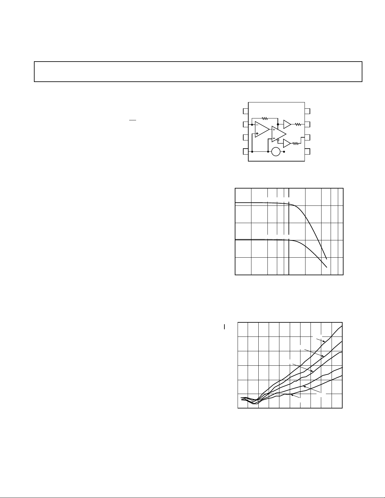
FUNCTIONAL BLOCK DIAGRAM
25.0E+3
20.0E+3
15.0E+3
1
NC
I
2
IN
3
NC
V
4
BYP
NC = NO CONNECT
AD8015
10kΩ
G = 30
+1
G = 3
+1
– + +V
1.7V
DIFFERENTIAL
50Ω
S
50Ω
+V
8
+OUTPUT
7
–OUTPUT
6
5
–V
S
S
PRODUCT DESCRIPTION
The AD8015 is a wide bandwidth, single supply transimpedance
amplifier optimized for use in a fiber optic receiver circuit. It is a
complete, single chip solution for converting photodiode current
into a differential voltage output. The 240MHz bandwidth enables
AD8015 application in FDDI receivers and SONET/SDH
receivers with data rates up to 155 Mbps. This high bandwidth
supports data rates beyond 300 Mbps. The differential outputs
drive ECL directly, or can drive a comparator/ fiber optic post
amplifier.
In addition to fiber optic applications, this low cost, silicon alternative to GaAs-based transimpedance amplifiers is ideal for
systems requiring a wide dynamic range preamplifier or singleended to differential conversion. The IC can be used with a
standard ECL power supply (–5.2 V) or a PECL (+5 V) power
supply; the common mode at the output is ECL compatible.
The AD8015 is available in die form, or in an 8-pin SOIC
package.
10.0E+3
X-RESISTANCE – Ω
5.0E+3
000.E+0
10.0E+6 100.0E+6 1.0E+9
SINGLE-ENDED
FREQUENCY – Hz
Figure 1. Differential/Single-Ended Transimpedance vs.
Frequency
5.0
Hz
√
4.5
4.0
3.5
3.0
2.5
EQUIVALENT INPUT CURRENT NOISE – pA
2.0
1.5pF
FREQUENCY – Hz
3.0pF
2.0pF
1.0pF
0.5pF
100.0E+620.0E+6000.0E+0 80.0E+660.0E+640.0E+6
REV. A
Information furnished by Analog Devices is believed to be accurate and
reliable. However, no responsibility is assumed by Analog Devices for its
use, nor for any infringements of patents or other rights of third parties
which may result from its use. No license is granted by implication or
otherwise under any patent or patent rights of Analog Devices.
Figure 2. Noise vs. Frequency (SO-8 Package with
Added Capacitance)
© Analog Devices, Inc., 1996
One Technology Way, P.O. Box 9106, Norwood, 02062-9106, U.S.A.
Tel: 617/329-4700 Fax: 617/326-8703
Page 2

AD8015–SPECIFICA TIONS
WARNING!
ESD SENSITIVE DEVICE
(SO Package @ TA = +258C and VS = +5 V, unless otherwise noted)
AD8015AR
Parameter Conditions Min Typ Max Units
DYNAMIC PERFORMANCE
Bandwidth 3 dB 180 240 MHz
Pulse Width Modulation 10 µA to 200 µA Peak 500 ps
Rise and Fall Time 10% to 90% 1.5 ns
Settling Time
1
to 3%, 0.5 V Diff Output Step 3 ns
INPUT
Linear Input Current Range ±2.5%, Nonlinearity ±25 ±30 µA
Max Input Current Range Saturation ±200 ±350 µA
Optical Sensitivity 155 Mbps, Avg Power –36 dBm
Input Stray Capacitance Die, by Design 0.2 pF
SOIC, by Design 0.4 pF
Input Bias Voltage +VS to I
NOISE Die, Single Ended at P
or Differential (P
C
STRAY
and V
IN
= 0.3 pF
BYP
OUT
OUT–NOUT
1.6 1.8 2.0 V
,
),
Input Current Noise f = 100 MHz 3.0 pA/√
Total Input RMS Noise DC to 100 MHz 26.5 nA
TRANSFER CHARACTERISTICS
Transresistance Single Ended 8 10 12 kΩ
Differential 16 20 24 kΩ
Power Supply Single Ended 37.0 dB
Rejection Ratio Differential 40 dB
Hz
OUTPUT
Differential Offset 620mV
Output Common-Mode Voltage From Positive Supply –1.5 –1.3 –1.1 V
Voltage Swing (Differential) Positive Input Current, R
Positive Input Current, R
= ∞ 1.0 V p-p
L
= 50 Ω 600 mV p-p
L
Output Impedance 40 50 60 Ω
POWER SUPPLY T
MIN
to T
MAX
Operating Range Single Supply +4.5 +5 +11 V
Dual Supply ±2.25 ±5.5 V
Current 25 26 mA
NOTES
1
Settling Time is defined as the time elapsed from the application of a perfect step input to the time when the output has entered and remained within a specified error
band symmetrical about the final value. This parameter includes propagation delay, slew time, overload recovery, and linear settling times.
Specifications subject to change without notice.
ABSOLUTE MAXIMUM RATINGS
Supply Voltage (+VS to –VS). . . . . . . . . . . . . . . . . . . . . . . 12 V
Internal Power Dissipation
2
1
Small Outline . . . . . . . . . . . . . . . . . . . . . . . . . . . . 0.9 Watts
Output Short Circuit Duration . . . . . . . . . . . . . . . Indefinite
Maximum Input Current . . . . . . . . . . . . . . . . . . . . . . . . 10 mA
Storage Temperature Range . . . . . . . . . . . . –65°C to +125°C
Operating Temperature Range (T
MIN
to T
MAX
)
AD8015ACHIP/AR . . . . . . . . . . . . . . . . . . –40°C to +85°C
Maximum Junction Temperature . . . . . . . . . . . . . . . . . +165°C
Lead Temperature Range (Soldering 10 sec) . . . . . . . . +300°C
NOTES
1
Stresses above those listed under “Absolute Maximum Ratings” may cause
permanent damage to the device. This is a stress rating only and functional
operation of the device at these or any other conditions above those indicated in the
operational section of this specification is not implied. Exposure to absolute
maximum rating conditions for extended periods may affect device reliability.
2
Specification is for device in free air: 8-pin SOIC package: θJA = 155°C/W.
ORDERING GUIDE
Temperature Package Package
Model Range Description Option
AD8015AR –40°C to +85°C 8-Pin Plastic SOIC SO-8
AD8015ACHIPS –40°C to +85°C Die Fo
rm
CAUTION
ESD (electrostatic discharge) sensitive device. Electrostatic charges as high as 4000 V readily
accumulate on the human body and test equipment and can discharge without detection.
Although the AD8015 features proprietary ESD protection circuitry, permanent damage may
occur on devices subjected to high energy electrostatic discharges. Therefore, proper ESD
precautions are recommended to avoid performance degradation or loss of functionality.
–2–
REV. A
Page 3
V1
+V
S
CLOCK
RECOVERY
LPF:
3dB@
0.7 x F
LPF:
3dB@
0.7 x F
QUANTIZER
R > 40Ω
C1 >100pF
4.5V < V
S
< 11V
CLK
DATA
RR
C1
10kΩ
5
6
7
8
4
3
2
1
AD8015
50Ω
+1
G = 3
G = 30
50Ω
+1
– + +V
S
1.7V
1.7V
+V
S
PIN CONFIGURATION
AD8015
AD8015
1
NC
I
IN
NC
V
BYP
10kΩ
2
G = 30
3
4
NC = NO CONNECT
G = 3
– + +V
1.7V
+1
50Ω
+1
S
METALIZATION PHOTOGRAPH
Dimensions shown in microns. Not to scale.
OPTIONAL
+V
CONNECTION
S
+V
50Ω
S
+V
8
+OUTPUT
7
–OUTPUT
6
5
–V
S
.
S
Figure 3. Fiber Optic Receiver Application: Photodiode
Referred to Positive Supply
PHOTODIODE REFERRED TO NEGATIVE SUPPLY
Figure 4 shows the AD8015 used in a circuit where the photodiode is referred to the negative supply. This results in a larger
back bias voltage than when referring the photodiode to the
positive supply. The larger back bias voltage on the photodiode
I
IN
V
BYP
NOTE:
FOR BEST PERFORMANCE ATTACH PACKAGE
SUBSTRATE TO +VS.
MATERIAL AT BACK OF DIE IS SILICON. USE OF
OR –VS FOR DIE ATTACH IS ACCEPTABLE.
+V
S
813µ
973µ
–V
S
+OUTPUT
838µ
998µ
–OUTPUT
decreases the photodiode’s capacitance thereby increasing its
bandwidth. The R2, C2 network shown in Figure 4 is added to
decouple the photodiode to the positive supply. This improves
PSRR.
+V
+V
S
C2
+V
S
1.7V
R2
1
2
3
4
AD8015
10kΩ
G = 30
G = 3
– + +V
1.7V
C1
50Ω
+1
50Ω
+1
S
S
LPF:
3dB@
0.7 x F
LPF:
3dB@
0.7 x F
V1
RR
RECOVERY
QUANTIZER
R > 40Ω
C1 >100pF
4.5V < V
R2 AND C2 OPTIONAL
FOR IMPROVED PSRR
< 11V
S
DATA
CLK
CLOCK
8
7
6
5
Figure 4. Fiber Optic Receiver Application: Photodiode
Referred to Negative Supply
FIBER OPTIC RECEIVER APPLICATIONS
In a fiber optic receiver, the photodiode can be placed from the
I
pin to either the positive or negative supply. The AD8015
IN
converts the current from the photodiode to a differential voltage in these applications. The voltage at the V
pin is ≈1.8 V
BYP
below the positive supply. This node must be bypassed with a
capacitor (C1 in Figures 3 and 4 below) to the signal ground. If
large levels of power supply noise exist, then connecting C1 to
+V
is recommended for improved noise immunity. For opti-
S
mum performance, choose C1 such that C1 > 1/(2 π × 1000 ×
f
); where f
MIN
is the minimum useful
MIN
frequency in Hz.
FIBER OPTIC SYSTEM NOISE PERFORMANCE
The AD8015 maintains 26.5 nA referred to input (RTI) to 100
MHz. Calculations below translate this specification into minimum power level and bit error rate specifications for SONET
and FDDI systems. The dominant sources of noise are: 10 kΩ
feedback resistor current noise, input bipolar transistor base
current noise, and input voltage noise.
The AD8015 has dielectrically isolated devices and bond pads
that minimize stray capacitance at the I
pin. Input voltage
IN
noise is negligible at lower frequencies, but can become the
dominant noise source at high frequencies due to I
capacitance. Minimizing the stray capacitance at the I
pin stray
IN
pin is
IN
critical to maintaining low noise levels at high frequencies. The
PHOTODIODE REFERRED TO POSITIVE SUPPLY
Figure 3 shows the AD8015 used in a circuit where the photodiode is referred to the positive supply. The back bias voltage on
the photodiode is ≈1.8 V. This method of referring the photodiode provides greater power supply noise immunity (PSRR)
than referring the photodiode to the negative supply. The signal
path is referred to the positive rail, and the photodiode capacitance is not modulated by high frequency noise that may exist
on the negative rail.
REV. A
pins surrounding the I
connection and should be left unconnected in an application.
This minimizes I
ground plane or metal runs near Pins 1, 2, and 3 and to minimize capacitance at the I
The AD8015AR (8-pin SOIC) I
0.4 pF without the photodiode. Photodiodes used for SONET
or FDDI systems typically add 0.3 pF, resulting in roughly
0.7 pF total stray capacitance.
–3–
pin (Pins 1 and 3) have no internal
IN
pin package capacitance. It is best to have no
IN
pin.
IN
pin total stray capacitance is
IN
Page 4

AD8015
SONET OC-3 SENSITIVITY ANALYSIS
OC-3 Minimum Bandwidth = 0.7 × 155 MHz ≈ 110 MHz
Total Current Noise = (π/2) × 26.5 nA
= 42 nA (assuming single pole response)
–10
To maintain a BER < 1 × 10
(1 error per 10 billion bits):
Minimum current level needs to be > 13 × Total Current Noise
= 541 nA (peak)
Assume a typical photodiode current/power conversion ratio
= 0.85 A/W
Sensitivity (minimum power level) = 541/0.85 nW
= 637 nW (peak)
= –32.0 dBm (peak)
= –35.0 dBm (average)
The SONET OC-3 specification allows for a minimum power
level of –31 dBm peak, or –34 dBm average. Using the AD8015
provides 1 dB margin.
FDDI SENSITIVITY ANALYSIS
FDDI Minimum Bandwidth = 0.7 × 125 MHz ≈ 88 MHz
Total Current Noise = (π /2)×
88 MHz
100 MHz
× 26.5nA
= 39 nA (assuming single pole response)
–10
To maintain a BER < 2.5 × 10
(1 error per 4 billion bits):
Minimum current level needs to be > 12.6 × Total Current Noise
= 492 nA (peak)
Assume a typical photodiode current/power conversion ratio
= 0.85 A/W
Sensitivity (minimum power level) = 492/0.85 nW
= 579 nW (peak)
= –32.4 dBm (peak)
= –35.4 dBm (average)
The FDDI specification allows for a minimum power level of
–28 dBm peak, or –31 dBm average. Using the AD8015 provides 4.4 dB margin.
THEORY OF OPERATION
The simplified schematic is shown in Figure 5. Q1 and Q3 make
up the input stage, with Q3 running at 300 µA and Q1 running
at 2.7 mA. Q3 runs essentially as a grounded emitter. A large
capacitor (0.01 µF) placed from V
to the positive supply
BYP
shorts out the noise of R17, R21, and Q16. The first stage of the
amplifier (Q3, R2, Q4, and C1) functions as an integrator, integrating current into the I
pin. The integrator drives a differen-
IN
tial stage (Q5, Q6, R5, R3, and R4) with gains of +3 and –3.
The differential stage then drives emitter followers (Q41, Q42,
Q60 and Q61). The positive output of the differential stage provides the feedback by driving R
. The differential outputs are
FB
buffered using Q7 and Q8.
The bandwidth of the AD8015 is set to within
+20% of the
nominal value, 240 MHz, by factory trimming R5 to 60 Ω. The
following formula describes the AD8015 bandwidth:
Bandwidth = 1/(2
π
× C1 × RFB × (R5 + 2 re)/R4)
where re (of Q5 and Q6) = 9 Ω each, constant over temperature,
and R
/R4 = 43.5, constant over temperature.
FB
The bandwidth equation simplifies, and the bandwidth depends
only on the value of C1:
Bandwidth = 1/(2 π × 3393 × C1).
V
BYP
1.5MA
I1
R21
1.8k
R17
635
Q16
R1
300
3MA
R2
3k
Q4
INPUT
CLAMPS
Q3
Q1
+V
S
I10
0.75MA
Q56
I2
I
IN
C1 0.2pF
I3
1MAI43MAI53MAI61MAI71MAI81MAI91MA
R3
R4
230
230
Q41
Q5
Q6
R5 60
RFB
10k
Figure 5. AD8015 Simplified Schematiic
–4–
+V
S
Q61
330
330
R44 50
Q60
R43 50
+OUTPUT
–OUTPUT
Q42
Q7
–V
S
Q8
REV. A
Page 5

AD8015
9
1
10 100
1000
5
0
4k
AD8015
V
OUT
IN
GAIN – dB
FREQUENCY – MHz
+85°C
–40°C AND 0°C
50Ω
9.0
7.0
5.0
10.0E+6 100.0E+6 1.0E+9
6.5
6.0
5.5
7.5
8.0
8.5
FREQUENCY – Hz
GAIN – dB
11.0V
5.0V
4.5V
1.5
1.0
0.5
0
–0.5
OUTPUT VOLTAGE – Volts
–1.0
–1.5
–80
–100
INPUT CURRENT – µA
+85°C
+ 25°C
– 40°C
804020060–20–40–60
100
Figure 6. Differential Output vs. Input Current
0
–0.5
PIN 7
–1.0
–1.5
PIN 6
OUTPUT VOLTAGE – Volts
–2.0
–2.5
–80
–100
+25°C
INPUT CURRENT – µA
+25°C
–40°C
+85°C
+85°C
–40°C
806040200–20–40–60
100
Figure 9. Gain vs. Frequency
10
5V, +25°C
0
GROUP DELAY – ns
10 100 1000
FREQUENCY – MHz
Figure 7. Single-Ended Output vs. Input Current
300
290
280
270
260
250
240
230
BANDWIDTH – MHz
220
210
200
–30
–40
Figure 8. Bandwidth vs. Temperature
TEMPERATURE – °C
Figure 10. Group Delay vs. Frequency
80
706050403020100–10–20
Figure 11. Differential Gain vs. Supply
REV. A
–5–
Page 6

AD8015
100
50
IMPEDANCE – Ω
0
1
5V, +25°C
PIN 7
PIN 6
10 100
FREQUENCY – MHz
Figure 12. Output Impedance vs. Frequency
100
0
VOLTAGE – mV
–100
10
TIME – ns
Figure 13. Small Signal Pulse Response
1000
200
APPLICATION
155 Mbps Fiber Optic Receiver
The AD8015 and AD807 can be used together for a complete
155 Mbps Fiber Optic Receiver (Transimpedance Amplifier,
Post Amplifier with Signal Detect Output, and Clock Recovery
and Data Retiming) as shown in Figure 16.
The PIN diode front end is connected to a single mode, 1300 nm
laser source. The PIN diode has 3.3 V reverse bias, 0.8 A/W
responsivity, 0.7 pF capacitance, and 2.5 GHz bandwidth.
The AD8015 outputs (P
OUT
and N
) drive a differential, con-
OUT
stant impedance (50 Ω) low-pass π filter with a 3 dB cutoff of
100 MHz. The outputs of the low-pass filter are ac coupled to
the AD807 inputs (PIN and NIN). The AD807 PLL damping
factor is set at 10 using a 0.22 µF capacitor.
The entire circuit was enclosed in a shielded box. Table I summarizes results of tests performed using a 2
23
–1 PRN sequence,
and varying the average power at the PIN diode.
The circuit acquires and maintains lock with an average input
power as low as –39.25 dBm.
30 DEVICES, 2 LOTS:
(+OUT, –OUT) × (25°C, –40°C, 85°C) × (5V, 4.5V, 11.0V)
80
70
60
50
40
30
POPULATION – Parts
20
10
0
100
90
80
70
60
50
40
CUMULATIVE – %
30
20
10
0
2
0
–2
–4
–6
GAIN – dB
–8
–10
–12
10.0E+6 100.0E+6 1.0E+9
5pF
8pF
FREQUENCY – Hz
1pF
0pF
3pF
Figure 14. Differential Gain vs. Input Capacitance
200.000E+6
205.000E+6
215.000E+6
220.000E+6
225.000E+6
230.000E+6
235.000E+6
240.000E+6
245.000E+6
250.000E+6
255.000E+6
260.000E+6
265.000E+6
270.000E+6
275.000E+6
280.000E+6
285.000E+6
290.000E+6
210.000E+6
FREQUENCY – Hz
295.000E+6
Figure 15. Bandwidth Distribution Matrix
300.000E+6
–6–
REV. A
Page 7

DATAOUTN
DATAOUTP
CLKOUTN
CLKOUTP
C2
0.1µF
C4
0.1µF
C5
0.1µF
0.1µF
C1
0.1µF
R1
100R2100
C3
0.1µF
R4
R3
100
100
C6
NOTES
1. ALL CAPS ARE CHIP,
15pF ARE MICA.
2. 150 nH ARE SMT
NC = NO CONNECT
R5 100
R6 100
R7 100
R8 100
R11
154
R11
154
C7
C8
CD
R12
154
DAMPING
CAP,0.22µF
R10
154
TP1
TP2
1
DATAOUTN
2
DATAOUTP
3
VCC2
4
CLKOUTN
5
CLKOUTP
6
VCC1
CF1
7
CF2
8
GND
TP4
ABB HAFO
1A227
FC HOUSING
THRADJ
AD807
C9
10µF
5V
TP3
0.8 A/W, 0.7pF
2.5GHz
0.1µF
TP8 TP7
100pF
16
V
EE
15
SDOUT
14
AVCC
13
PIN
12
NIN
11
AVCC
10
9
AVEE
NC
1
I
2
IN
NC
3
V
4
BYP
AD8015
0.01µF
C1
SDOUT
3.65k
C10
100
pF
+V
S
+OUT
–OUT
–V
R17
C11
TP6
S
C12
2.2µF
R13
THRADJ
TP5
8
7
6
5
0.1µF
10µF
150nH
15pF
150nH
R16
301
C15
0.1µF
15pF
R14
50
0.1µF
50Ω
LINE
C14
R15
50
50Ω
LINE
AD8015
C13
0.1µF
Figure 16. 155 Mbps Fiber Optic Receiver Schematic
Table I. AD8015, AD807 Fiber Optic Receiver Circuit:
Output Bit Error Rate & Output Jitter vs. Average Input Power
Average Optical Output Bit Output Jitter
Input Power (dBm) Error Rate (ps rms)
–6.4 Loses Lock
–6.45 1.2 × 10
–6.50 7.5 × 10
–6.60 9.4 × 10
–6.70 1 × 10
–7.0 to 1 × 10
–35.50
–36.00 3.0 × 10
–36.50 4.8 × 10
–37.00 2.8 × 10
–37.50 8.2 × 10
–38.00 1.3 × 10
–38.50 1.1 × 10
–39.00 1.0 × 10
–39.1 1.3 × 10
–39.20 1.9 × 10
–39.25 2.2 × 10
–14
–14
–2
–3
–4
–12
–10
–8
–7
–5
–4
–3
–3
–3
–3
< 40
< 40
–39.30 Loses Lock
REV. A
–7–
Page 8

AD8015
AC COUPLED PHOTODIODE APPLICATION FOR
IMPROVED DYNAMIC RANGE
AC coupling the photodiode current input to the AD8015 (Figure 17) extends fiber optic receiver overload by 3 dB while sacrificing only 1 dB of sensitivity (increasing receiver dynamic range
by 2 dB). This application results in typical overload of –4 dBm,
+V
S
AD8015
1
C
AC
0.01µF
R
AC
7k
10kΩ
2
G = 30
3
4
+1
G = 3
+1
– + +V
1.7V
C1
8
50Ω
7
6
50Ω
5
S
Figure 17. AC Coupled Photodiode Application for Improved Dynamic Range
and typical sensitivity of –35 dBm. AC coupling the input also
results in improved pulse width modulation performance.
Careful attention to minimize parasitic capacitance at the
AD8015 input (from the photodetector input), R
and CAC are
AC
critical for sensitivity performance in this application. Note that
C
of 0.01 µF was chosen for a low frequency cutoff equal to
AC
2.2 kHz.
+V
S
V1
LPF:
R
3dB@
0.7 x F
LPF:
3dB@
0.7 x F
R
CLOCK
RECOVERY
QUANTIZER
R > 40Ω
C1 >100pF
4.5V < V
< 11V
S
CLK
DATA
C1973–6–1/96
OUTLINE DIMENSIONS
Dimensions shown in inches and (mm).
8-Lead Small Outline IC Package (SO-8)
0.1968 (5.00)
0.1890 (4.80)
8
0.0500
(1.27)
BSC
5
0.2440 (6.20)
41
0.2284 (5.80)
0.0688 (1.75)
0.0532 (1.35)
0.020 (0.51)
0.013 (0.33)
0.0098 (0.25)
0.0075 (0.19)
0.0196 (0.50)
0.0099 (0.25)
8°
0°
0.0500 (1.27)
0.0160 (0.41)
0.1574 (4.00)
0.1497 (3.80)
PIN 1
0.0098 (0.25)
0.0040 (0.10)
SEATING
PLANE
x 45°
PRINTED IN U.S.A.
–8–
REV. A
 Loading...