

Page 1
400 MHz Low Power
1
V
OUT
AD8014
–V
S
+IN
2
34
5
+V
S
–IN
a
FEATURES
Low Cost
Low Power: 1.15 mA Max for 5 V Supply
High Speed
400 MHz, –3 dB Bandwidth (G = +1)
4000 V/s Slew Rate
60 ns Overload Recovery
Fast Settling Time of 24 ns
Drive Video Signals on 50 ⍀ Lines
Very Low Noise
3.5 nV/√Hz and 5 pA/√Hz
5 nV/√Hz Total Input Referred Noise @ G = +3 w/500 ⍀
Feedback Resistor
Operates on +4.5 V to +12 V Supplies
Low Distortion –70 dB THD @ 5 MHz
Low, Temperature-Stable DC Offset
Available in SOIC-8 and SOT-23-5
APPLICATIONS
Photo-Diode Preamp
Professional and Portable Cameras
Hand Sets
DVD/CD
Handheld Instruments
A-to-D Driver
Any Power-Sensitive High Speed System
PRODUCT DESCRIPTION
The AD8014 is a revolutionary current feedback operational
amplifier that attains new levels of combined bandwidth, power,
output drive and distortion. Analog Devices, Inc. uses a proprietary circuit architecture to enable the highest performance
amplifier at the lowest power. Not only is it technically superior,
but is low priced, for use in consumer electronics. This general
purpose amplifier is ideal for a wide variety of applications
including battery operated equipment.
High Performance Amplifier
AD8014
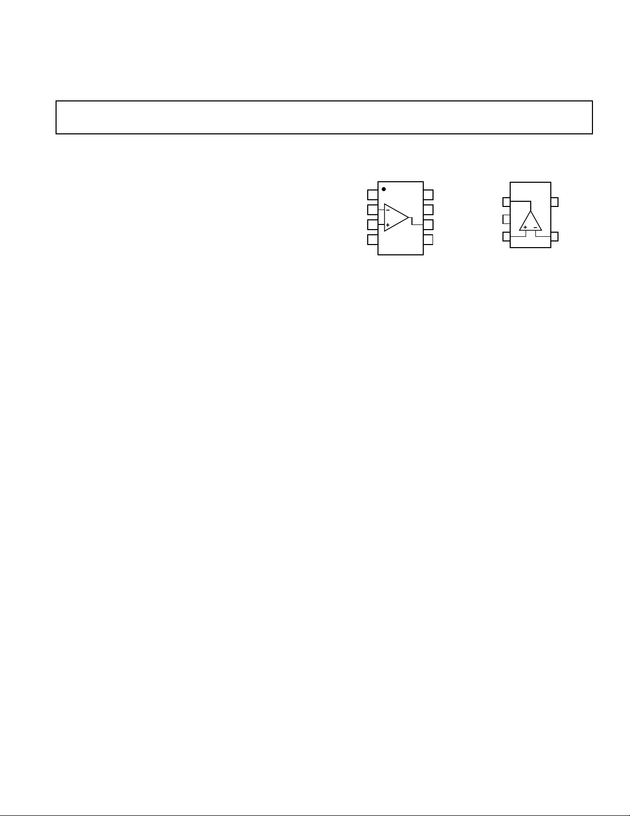
FUNCTIONAL BLOCK DIAGRAMS
SOIC-8 (R)
NC
1
–IN
2
+IN
3
4
–V
S
NC = NO CONNECT
AD8014
NC
8
+V
S
7
V
6
OUT
NC
5
The AD8014 is a very high speed amplifier with 400 MHz,
–3 dB bandwidth, 4000 V/µs slew rate, and 24 ns settling time.
The AD8014 is a very stable and easy to use amplifier with fast
overload recovery. The AD8014 has extremely low voltage and
current noise, as well as low distortion, making it ideal for use
in wide-band signal processing applications.
For a current feedback amplifier, the AD8014 has extremely
low offset voltage and input bias specifications as well as low
drift. The input bias current into either input is less than 15 µA
at +25°C with a typical drift of less than 50 nA/°C over the
industrial temperature range. The offset voltage is 5 mV max
with a typical drift less than 10 µV/°C.
For a low power amplifier, the AD8014 has very good drive
capability with the ability to drive 2 V p-p video signals on
75 Ω or 50 Ω series terminated lines and still maintain more
than 135 MHz, 3 dB bandwidth.
SOT-23-5 (RT)
REV. B
Information furnished by Analog Devices is believed to be accurate and
reliable. However, no responsibility is assumed by Analog Devices for its
use, nor for any infringements of patents or other rights of third parties
which may result from its use. No license is granted by implication or
otherwise under any patent or patent rights of Analog Devices.
One Technology Way, P.O. Box 9106, Norwood, MA 02062-9106, U.S.A.
Tel: 781/329-4700 World Wide Web Site: http://www.analog.com
Fax: 781/326-8703 © Analog Devices, Inc., 1999
Page 2

AD8014–SPECIFICATIONS
(@ TA = +25ⴗC, VS = ⴞ5 V, RL = 150 ⍀, RF = 1 k⍀, Gain = +2, unless otherwise noted)
AD8014AR/RT
Parameter Conditions Min Typ Max Units
DYNAMIC PERFORMANCE
–3 dB Bandwidth Small Signal G = +1, V
G = –1, V
–3 dB Bandwidth Large Signal V
0.1 dB Small Signal Bandwidth V
0.1 dB Large Signal Bandwidth V
Slew Rate, 25% to 75%, V
= 4 V Step R
O
= 2 V p-p 140 180 MHz
O
= 2 V p-p, R
V
O
= 2 V p-p, R
V
O
= 0.2 V p-p, R
O
= 2 V p-p, R
O
= 1 kΩ, RF = 500 Ω 4600 V/µs
L
= 1 kΩ 2800 V/µs
R
L
G = –1, R
G = –1, R
Settling Time to 0.1% G = +1, V
= 0.2 V p-p, R
O
= 0.2 V p-p, R
O
= 500 Ω 170 210 MHz
F
= 500 Ω, RL = 50 Ω 130 MHz
F
= 1 kΩ 12 MHz
L
= 1 kΩ 20 MHz
L
= 1 kΩ, RF = 500 Ω 4000 V/µs
L
= 1 kΩ 2500 V/µs
L
= 2 V Step, R
O
= 1 kΩ 400 480 MHz
L
= 1 kΩ 120 160 MHz
L
= 1 kΩ 24 ns
L
Rise and Fall Time 10% to 90% 2 V Step 1.6 ns
G = –1, 2 V Step 2.8 ns
Overload Recovery to Within 100 mV 0 V to ±4 V Step at Input 60 ns
NOISE/HARMONIC PERFORMANCE
Total Harmonic Distortion f
SFDR f
= 5 MHz, VO = 2 V p-p, R
C
= 5 MHz, VO = 2 V p-p –51 dB
f
C
= 20 MHz, VO = 2 V p-p –45 dB
f
C
= 20 MHz, VO = 2 V p-p –48 dB
C
= 1 kΩ –68 dB
L
Input Voltage Noise f = 10 kHz 3.5 nV/√Hz
Input Current Noise f = 10 kHz 5 pA/√Hz
Differential Gain Error NTSC, G = +2, R
NTSC, G = +2, R
Differential Phase Error NTSC, G = +2, R
NTSC, G = +2, R
= 500 Ω 0.05 %
F
= 500 Ω, RL = 50 Ω 0.46 %
F
= 500 Ω 0.30 Degree
F
= 500 Ω, RL = 50 Ω 0.60 Degree
F
Third Order Intercept f = 10 MHz 22 dBm
DC PERFORMANCE
Input Offset Voltage 25mV
T
MIN–TMAX
26mV
Input Offset Voltage Drift 10 µV/°C
Input Bias Current +Input or –Input 5 15 µA
Input Bias Current Drift 50 nA/°C
Input Offset Current 5 ±µA
Open Loop Transresistance 800 1300 kΩ
INPUT CHARACTERISTICS
Input Resistance +Input 450 kΩ
Input Capacitance +Input 2.3 pF
Input Common-Mode Voltage Range ±3.8 ±4.1 V
Common-Mode Rejection Ratio V
= ±2.5 V –52 –57 dB
CM
OUTPUT CHARACTERISTICS
Output Voltage Swing R
Output Current V
= 150 Ω±3.4 ±3.8 V
L
= 1 kΩ±3.6 ±4.0 V
R
L
= ±2.0 V 40 50 mA
O
Short Circuit Current 70 mA
Capacitive Load Drive for 30% Overshoot 2 V p-p, R
= 1 kΩ, RF = 500 Ω 40 pF
L
POWER SUPPLY
Operating Range ±2.25 ±5 ±6.0 V
Quiescent Current 1.15 1.3 mA
Power Supply Rejection Ratio ±4 V to ±6 V –55 –58 dB
Specifications subject to change without notice.
–2– REV. B
Page 3

AD8014
SPECIFICATIONS
Parameter Conditions Min Typ Max Units
DYNAMIC PERFORMANCE
–3 dB Bandwidth Small Signal G = +1, V
–3 dB Bandwidth Large Signal V
0.1 dB Small Signal Bandwidth V
0.1 dB Large Signal Bandwidth V
Slew Rate, 25% to 75%, V
Settling Time to 0.1% G = +1, V
Rise and Fall Time 10% to 90% 2 V Step 1.9 ns
Overload Recovery to Within 100 mV 0 V to ±2 V Step at Input 60 ns
NOISE/HARMONIC PERFORMANCE
Total Harmonic Distortion f
SFDR f
Input Voltage Noise f = 10 kHz 3.5 nV/√Hz
Input Current Noise f = 10 kHz 5 pA/√Hz
Differential Gain Error NTSC, G = +2, R
Differential Phase Error NTSC, G = +2, R
Third Order Intercept f = 10 MHz 22 dBm
DC PERFORMANCE
Input Offset Voltage 25mV
Input Offset Voltage Drift 10 µV/°C
Input Bias Current +Input or –Input 5 15 µA
Input Bias Current Drift 50 nA/°C
Input Offset Current 5 ±µA
Open Loop Transresistance 750 1300 kΩ
INPUT CHARACTERISTICS
Input Resistance +Input 450 kΩ
Input Capacitance +Input 2.3 pF
Input Common-Mode Voltage Range 1.2 1.1 to 3.9 3.8 V
Common-Mode Rejection Ratio V
OUTPUT CHARACTERISTICS
Output Voltage Swing R
Output Current V
Short Circuit Current 70 mA
Capacitive Load Drive for 30% Overshoot 2 V p-p, R
POWER SUPPLY
Operating Range 4.5 5 12 V
Quiescent Current 1.0 1.15 mA
Power Supply Rejection Ratio 4 V to 5.5 V –55 –58 dB
Specifications subject to change without notice.
(@ TA = +25ⴗC, VS = +5 V, RL = 150 ⍀, RF = 1 k⍀, Gain = +2, unless otherwise noted)
AD8014AR/RT
= 2 V Step R
O
= 0.2 V p-p, R
O
G = –1, V
= 2 V p-p 75 100 MHz
O
= 2 V p-p, R
V
O
= 2 V p-p, R
V
O
= 0.2 V p-p, R
O
= 2 V p-p 20 MHz
O
= 1 kΩ, RF = 500 Ω 3900 V/µs
L
= 1 kΩ 1100 V/µs
R
L
G = –1, R
G = –1, R
= 0.2 V p-p, R
O
= 500 Ω 90 115 MHz
F
= 500 Ω, RL = 75 Ω 100 MHz
F
= 1 kΩ 10 MHz
L
= 1 kΩ, RF = 500 Ω 1800 V/µs
L
= 1 kΩ 1100 V/µs
L
= 2 V Step, R
O
= 1 kΩ 345 430 MHz
L
= 1 kΩ 100 135 MHz
L
= 1 kΩ 24 ns
F
G = –1, 2 V Step 2.8 ns
= 5 MHz, VO = 2 V p-p, R
C
= 5 MHz, VO = 2 V p-p –51 dB
f
C
= 20 MHz, VO = 2 V p-p –45 dB
f
C
= 20 MHz, VO = 2 V p-p –47 dB
C
= 500 Ω 0.06 %
F
NTSC, G = +2, R
NTSC, G = +2, R
T
MIN–TMAX
= 1.5 V to 3.5 V –52 –57 dB
CM
= 150 Ω to 2.5 V 1.4 1.1 to 3.9 3.6 V
L
= 1 kΩ to 2.5 V 1.2 0.9 to 4.1 3.8 V
R
L
= 1.5 V to 3.5 V 30 50 mA
O
= 1 kΩ, RF = 500 Ω 55 pF
L
= 500 Ω, RL = 50 Ω 0.05 %
F
= 500 Ω 0.03 Degree
F
= 500 Ω, RL = 50 Ω 0.30 Degree
F
= 1 kΩ –70 dB
L
26mV
–3–REV. B
Page 4

AD8014
WARNING!
ESD SENSITIVE DEVICE
ABSOLUTE MAXIMUM RATINGS
Supply Voltage . . . . . . . . . . . . . . . . . . . . . . . . . . . . . . . .12.6 V
Internal Power Dissipation
2
1
Small Outline Package (R) . . . . . . . . . . . . . . . . . . . . 0.75 W
SOT-23-5 Package (RT) . . . . . . . . . . . . . . . . . . . . . . 0.5 W
Input Voltage Common Mode . . . . . . . . . . . . . . . . . . . . . .±V
S
Differential Input Voltage . . . . . . . . . . . . . . . . . . . . . . ±2.5 V
Output Short Circuit Duration
. . . . . . . . . . . . . . . . . . . . . . Observe Power Derating Curves
Storage Temperature Range . . . . . . . . . . . . –65°C to +150°C
Operating Temperature Range . . . . . . . . . . . –40°C to +85°C
Lead Temperature (Soldering 10 sec) . . . . . . . . . . . . .+300°C
ESD (Human Body Model) . . . . . . . . . . . . . . . . . . . . +1500 V
NOTES
1
Stresses above those listed under Absolute Maximum Ratings may cause permanent damage to the device. This is a stress rating only, functional operation of the
device at these or any other conditions above listed in the operational section of this
specification is not implied. Exposure to Absolute Maximum Ratings for any
extended periods may affect device reliability.
2
Specification is for device in free air at 25°C.
8-Lead SOIC Package θ
5-Lead SOT-23 Package θ
= 155°C/W.
JA
= 240°C/W.
JA
MAXIMUM POWER DISSIPATION
The maximum power that can be safely dissipated by the AD8014
is limited by the associated rise in junction temperature. The
maximum safe junction temperature for plastic encapsulated
devices is determined by the glass transition temperature of the
plastic. This is approximately +150°C. Even temporarily ex-
ceeding this limit may cause a shift in parametric performance
due to a change in the stresses exerted on the die by the pack-
age. Exceeding a junction temperature of +175°C may result in
device failure.
The output stage of the AD8014 is designed for large load current capability. As a result, shorting the output to ground or to
power supply sources may result in a very large power dissipation. To ensure proper operation it is necessary to observe the
maximum power derating tables.
Table I. Maximum Power Dissipation vs. Temperature
Ambient Temp Power Watts Power Watts
ⴗC SOT-23-5 SOIC
–40 0.79 1.19
–20 0.71 1.06
0 0.63 0.94
+20 0.54 0.81
+40 0.46 0.69
+60 0.38 0.56
+80 0.29 0.44
+100 0.21 0.31
ORDERING GUIDE
Model Temperature Range Package Descriptions Package Options Brand Code
AD8014AR
AD8014ART
AD8014AChips
NOTES
1
The AD8014AR is also available in 13" Reels of 2500 each and 7" Reels of 750 each.
2
Except for samples, the AD8014ART is only available in 7" Reels of 3000 each and 13" Reels of 10000 each.
3
The AD8014A Chips are available only in Waffle Pak of 400 each. The thickness of the AD8014A Chip is 12␣ mils ±1 mil. The Substrate should be tied to the +V
source.
1
2
–40°C to +85°C 8-Lead SOIC SO-8 Standard
–40°C to +85°C 5-Lead SOT-23 RT-5 HAA
3
–40°C to +85°C Not Applicable Waffle Pak Not Applicable
CAUTION
ESD (electrostatic discharge) sensitive device. Electrostatic charges as high as 4000 V readily
accumulate on the human body and test equipment and can discharge without detection.
Although the AD8014 features proprietary ESD protection circuitry, permanent damage may
occur on devices subjected to high energy electrostatic discharges. Therefore, proper ESD
precautions are recommended to avoid performance degradation or loss of functionality.
S
–4– REV. B
Page 5

Typical Performance Characteristics–
FREQUENCY – MHz
2.0
–7.0
1 100010010
–6.0
–5.0
–4.0
–3.0
–1.0
0
1.0
–2.0
NORMALIZED GAIN – dB
VS = 65V
G = –1
R
F
= 1kV
R
L
= 1kV
VO = 2V
VO = 4V
VO = 0.2V
VO = 0.5V
VO = 1V
FREQUENCY – MHz
12
1 100010010
–12
–9
–6
–3
3
6
9
0
NORMALIZED GAIN – dB
VS = +5V
G = +2
R
F
= 1kV
R
L
= 1kV
VO = 1V p-p
VO = 3V p-p
VO = 2V p-p
VO = 0.5V p-p
FREQUENCY – MHz
2
1 100010010
–8
–7
–5
–4
–2
0
1
–3
–6
–1
NORMALIZED GAIN – dB
VS = +5V
G = –1
R
F
= 1kV
R
L
= 1kV
VO = 2V p-p
VO = 0.2V p-p
VO = 4V p-p
VO = 0.5V p-p
15
G = +1
12
VO = 200mV p-p
= 1kV
R
9
F
R
= 1kV
L
6
3
0
–3
–6
NORMALIZED GAIN – dB
–9
–12
–15
1 100010010
FREQUENCY – MHz
Figure 1. Frequency Response, G = +1, VS = ±5 V and +5 V
12
9
6
3
VS = 65V
G = +2
0
R
= 500V
F
V
= 2V p-p
–3
O
–6
NORMALIZED GAIN – dB
–9
–12
–15
1 100010010
FREQUENCY – MHz
VS = 65V
VS = +5V
RL = 75V
RL = 50V
AD8014
Figure 4. Bandwidth vs. Output Level—Gain of –1, Dual
Supply
Figure 2. Frequency Response, G = +2, VO = 2 V p-p
12
9
6
3
0
–3
NORMALIZED GAIN – dB
VS = 65V
–6
G = +2
= 1kV
R
F
–9
R
= 1kV
L
–12
10
VO = 4V p-p
VO = 2V p-p
100
FREQUENCY – MHz
VO = 0.5V p-p
VO = 1V p-p
1000
Figure 3. Bandwidth vs. Output Voltage Level—
Dual Supply, G = +2
Figure 5. Bandwidth vs. Output Level—Single Supply,
G = +2
Figure 6. Bandwidth vs. Output Level—Single Supply,
Gain of –1
–5–REV. B
Page 6

AD8014
G = +2
V = 2V p-p
RF = 500V
R
L
= 150V
FREQUENCY – MHz
1 100010010
5.3
5.8
5.4
5.9
VS = 65V
VS = +5V
6.2
5.2
5.5
5.6
6.0
6.1
5.7
GAIN FLATNESS – dB
VS = ±5V
R
F
= 1kV
R
L
= 1kV
V
O
= 200mV p-p
1 100010010
–15
–3
–12
0
G = +1
G = +2
9
–18
–9
3
6
–6
G = +10
FREQUENCY – MHz
GAIN – dB
7.5
7.0
6.5
6.0
5.5
5.0
4.5
VS = 65V
NORMALIZED GAIN – dB
4.0
G = +2
= 2V p-p
V
O
3.5
R
= 150V
L
3.0
1 100010010
Figure 7. Bandwidth vs. Feedback Resistor—Dual Supply
7.5
7.0
RF = 300V
RF = 500V
RF = 600V
RF = 750V
RF = 1kV
FREQUENCY – MHz
Figure 10. Gain Flatness—Large Signal
Figure 8. Bandwidth vs. Feedback Resistor—Single Supply
6.5
6.0
5.5
5.0
VS = +5V
NORMALIZED GAIN – dB
G = +2
= 2V p-p
V
4.5
O
R
= 150V
L
4.0
1 100010010
6.8
G = +2
6.7
RF = 1kV
6.6
R
= 1kV
L
6.5
V
= 200mV p-p
O
6.4
6.3
6.2
6.1
6.0
NORMALIZED GAIN – dB
5.9
5.8
5.7
5.6
1 100010010
RF = 500V
RF = 750V
FREQUENCY – MHz
FREQUENCY – MHz
RF = 300V
RF = 1kV
VS = +5V
Figure 9. Gain Flatness—Small Signal
VS = 65V
Figure 11. Bandwidth vs. Gain—Dual Supply, RF = 1 k
9
6
3
0
VS = +5V
–3
R
= 1kV
F
R
= 1kV
L
–6
GAIN – dB
V
= 200mV p-p
O
–9
–12
–15
–18
1 100010010
G = +2
G = +10
FREQUENCY – MHz
G = +1
Ω
Figure 12. Bandwidth vs. Gain—Single Supply
–6– REV. B
Page 7

AD8014
g
FREQUENCY – MHz
100
10
1
0.1
0.01
1
1000
10 1000.1
0.01
OUTPUT RESISTANCE – V
0
–10
VS = 65V
–20
G = +2
R
–30
–40
–50
PSRR – dB
–60
–70
–80
–90
–100
0.01
–20
–25
–30
–35
–40
–45
–50
CMRR – dB
–55
–60
–65
–70
–75
0.1
= 1kV
F
0.10
–PSRR
+PSRR
1 10 100
FREQUENCY – MHz
Figure 13. PSRR vs. Frequency
VS = +5V
VS = ±5V
1 10 100
FREQUENCY – MHz
Figure 14. CMRR vs. Frequency
1000
1000
140
120
100
80
60
GAIN – dBV
40
20
0
1k 10k 100k 1M 10M 100M 1G
FREQUENCY – Hz
PHASE
GAIN
0
–40
–80
–120
–160
–200
–240
–280
Figure 16. Transimpedance Gain and Phase vs.
Frequency
Figure 17. Output Resistance vs. Frequency, VS = ±5 V
and +5 V
rees
PHASE – De
–30
3RD
RL = 150V
–50
2ND
RL = 150V
–70
DISTORTION – dBc
3RD
RL = 1kV
DISTORTION BELOW
NOISE FLOOR
–90
1 10010
FREQUENCY – MHz
Figure 15. Distortion vs. Frequency; V
2ND
RL = 1kV
= ±5 V, G = +2
S
␣␣
Figure 18. Settling Time
–7–REV. B
Page 8

AD8014
Figure 19. Large Signal Step Response; VS = ±5 V,
V
= 4 V Step
O
Figure 21 shows the circuit that was used to imitate a photodiode preamp. A photodiode for this application is basically a
high impedance current source that is shunted by a small capacitance. In this case, a high voltage pulse from a Picosecond
Pulse Labs Generator that is ac-coupled through a 20 kΩ resis-
tor is used to simulate the high impedance current source of a
photodiode. This circuit will convert the input voltage pulse into
a small charge package that is converted back to a voltage by the
AD8014 and the feedback resistor.
In this case the feedback resistor chosen was 1.74 kΩ, which is a
compromise between maintaining bandwidth and providing
sufficient gain in the preamp stage. The circuit preserves the
pulse shape very well with very fast rise time and a minimum of
overshoot as shown in Figure 22.
1.74kV
+5V
0.1mF
INPUT
20kV
49.9V
AD8014
–5V
49.9V
OUTPUT
(103 PROBE)
(NO LOAD)
Figure 21. AD8014 as a Photodiode Preamp
Figure 20. Large Signal Step Response; VS = +5 V,
V
= 2 V Step
O
Note: On Figures 19 and 20 R
= 500 Ω, RS = 50 Ω and C
F
=
L
20 pF.
APPLICATIONS
CD ROM and DVD Photodiode Preamp
High speed Multi-X CD ROM and DVD drives require high
frequency photodiode preamps for their read channels. To minimize the effects of the photodiode capacitance, the low impedance of the inverting input of a current feedback amplifier is
advantageous. Good group delay characteristics will preserve the
pulse response of these pulses. The AD8014, having many advantages, can make an excellent low cost, low noise, low power,
and high bandwidth photodiode preamp for these applications.
INPUT
20mV/DIV
OUTPUT
500mV/DIV
TEK RUN: 2.0GS/s ET AVERAGE
1
2
CH1 20.0V CH2 500mV M 25.0ns CH4 380mV
T[ ]
Figure 22. Pulse Response
–8– REV. B
Page 9

AD8014
40
30
20
010152025
CL – pF
10
R
SERIES
– V
5
Video Drivers
The AD8014 easily drives series terminated cables with video
signals. Because the AD8014 has such good output drive you
can parallel two or three cables driven from the same AD8014.
Figure 23 shows the differential gain and phase driving one
video cable. Figure 24 shows the differential gain and phase
driving two video cables. Figure 25 shows the differential gain
and phase driving three video cables.
0.00 0.02 0.04 0.05 0.05 0.05 0.04 0.04 0.04 0.04 0.03
0.10
0.05
0.00
–0.05
–0.10
DIFFERENTIAL GAIN – %
0.00 0.01 0.10 0.21 0.26 0.28 0.29 0.30 0.30 0.30 0.30
0.60
0.40
0.20
0.00
–0.20
–0.40
DIFFERENTIAL
PHASE – Degrees
–0.60
1ST 2ND 3RD 4TH 5TH 6TH 7TH 8TH 9TH 10TH 11TH
DRIVING CAPACITIVE LOADS
The AD8014 was designed primarily to drive nonreactive loads.
If driving loads with a capacitive component is desired, best
settling response is obtained by the addition of a small series
resistance as shown in Figure 26. The accompanying graph
shows the optimum value for R
vs. Capacitive Load. It is
SERIES
worth noting that the frequency response of the circuit when
driving large capacitive loads will be dominated by the passive
roll-off of R
SERIES
and CL.
Figure 23. Differential Gain and Phase RF = 500, ±5 V, RL =
150
Ω
, Driving One Cable, G = +2
0.00 –0.02 0.03 0.05 0.06 0.06 0.05 0.05 0.07 0.10 0.14
0.30
0.20
0.10
0.00
–0.10
–0.20
–0.30
DIFFERENTIAL GAIN – %
0.00 0.07 0.24 0.40 0.43 0.44 0.43 0.40 0.35 0.26 0.16
0.60
0.40
0.20
0.00
–0.20
–0.40
DIFFERENTIAL
PHASE – Degrees
–0.60
1ST 2ND 3RD 4TH 5TH 6TH 7TH 8TH 9TH 10TH 11TH
Figure 24. Differential Gain and Phase RF = 500, ±5 V, RL =
75
Ω
, Driving Two Cables, G = +2
Choosing Feedback Resistors
Changing the feedback resistor can change the performance of
the AD8014 like any current feedback op amp. The table below
illustrates common values of the feedback resistor and the performance which results.
Gain R
+1 1 kΩ Open 480 430
+2 1 kΩ 1 kΩ 280 260
+10 1 kΩ 111 Ω 50 45
Figure 26. Driving Capacitive Load
Table II.
–3 dB BW –3 dB BW
= ⴞ0.2 V VO = ⴞ0.2 V
V
F
R
G
O
RL = 1 k⍀ RL = 150 ⍀
–1 1 kΩ 1 kΩ 160 150
0.00 0.44 0.52 0.54 0.52 0.52 0.50 0.48 0.47 0.44 0.45
0.80
0.60
0.40
0.20
0.00
–0.20
–0.40
–0.60
–0.80
DIFFERENTIAL GAIN – %
0.00 0.10 0.32 0.53 0.57 0.59 0.58 0.56 0.54 0.51 0.48
0.80
0.60
0.40
0.20
0.00
–0.20
–0.40
DIFFERENTIAL
–0.60
PHASE – Degrees
–0.80
1ST 2ND 3RD 4TH 5TH 6TH 7TH 8TH 9TH 10TH 11TH
Figure 25. Differential Gain and Phase RF = 500, ±5 V, RL =
50
Ω
, Driving Three Cables, G = +2
–2 1 kΩ 499 Ω 140 130
–10 1 kΩ 100 Ω 45 40
+2 2 kΩ 2 kΩ 200* 180*
+2 750 Ω 750 Ω 260* 210*
+2 499 Ω 499 Ω 280* 230*
*V
= ±1 V.
O
–9–REV. B
Page 10

AD8014
0.1574 (4.00)
0.1497 (3.80)
PIN 1
0.0098 (0.25)
0.0040 (0.10)
OUTLINE DIMENSIONS
Dimensions shown in inches and (mm).
8-Lead Plastic SOIC
(SO-8)
0.1968 (5.00)
0.1890 (4.80)
8
5
0.2440 (6.20)
41
0.2284 (5.80)
0.0688 (1.75)
0.0532 (1.35)
0.0196 (0.50)
0.0099 (0.25)
C3439b–0–12/99
x 45°
0.0669 (1.70)
0.0590 (1.50)
0.0512 (1.30)
0.0354 (0.90)
0.0059 (0.15)
0.0019 (0.05)
SEATING
PLANE
0.0500
(1.27)
BSC
0.0192 (0.49)
0.0138 (0.35)
0.0098 (0.25)
0.0075 (0.19)
8°
0°
0.0500 (1.27)
0.0160 (0.41)
5-Lead Plastic Surface Mount (SOT-23)
(RT-5)
0.1181 (3.00)
0.1102 (2.80)
4 5
0.1181 (3.00)
0.1024 (2.60)
0.0374 (0.95) BSC
0.0571 (1.45)
0.0374 (0.95)
SEATING
PLANE
108
08
PIN 1
1 3
2
0.0748 (1.90)
BSC
0.0197 (0.50)
0.0138 (0.35)
0.0079 (0.20)
0.0031 (0.08)
0.0217 (0.55)
0.0138 (0.35)
–10– REV. B
PRINTED IN U.S.A.
 Loading...