

Page 1
Single Supply, Low Power,
1
2
3
4
5
6
7
14
13
12
11
10
9
8
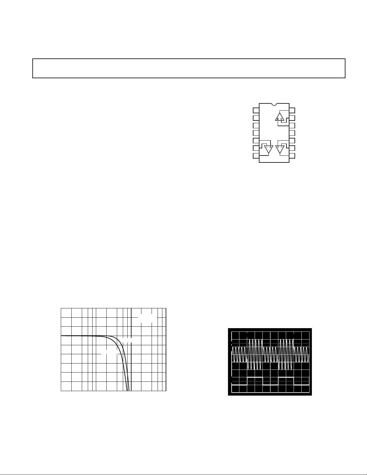
AD8013
OUT 2
–IN 2
+IN 2
–V
S
+IN 3
–IN 3
OUT 3
DISABLE 1
DISABLE 2
DISABLE 3
+V
S
+IN 1
–IN 1
OUT 1
a
FEATURES
Three Video Amplifiers in One Package
Drives Large Capacitive Load
Excellent Video Specifications (R
Gain Flatness 0.1 dB to 60 MHz
0.02% Differential Gain Error
0.06° Differential Phase Error
Low Power
Operates on Single +5 V to +13 V Power Supplies
4 mA/Amplifier Max Power Supply Current
High Speed
140 MHz Unity Gain Bandwidth (3 dB)
Fast Settling Time of 18 ns (0.1%)
1000 V/ms Slew Rate
High Speed Disable Function per Channel
Turn-Off Time 30 ns
Easy to Use
95 mA Short Circuit Current
Output Swing to Within 1 V of Rails
APPLICATIONS
LCD Displays
Video Line Driver
Broadcast and Professional Video
Computer Video Plug-In Boards
Consumer Video
RGB Amplifier in Component Systems
PRODUCT DESCRIPTION
The AD8013 is a low power, single supply, triple video
amplifier. Each of the three amplifiers has 30 mA of output
current, and is optimized for driving one back terminated video
load (150 Ω) each. Each amplifier is a current feedback amplifier and features gain flatness of 0.1 dB to 60 MHz while offering
0.2
0.1
0
–0.1
–0.2
–0.3
NORMALIZED GAIN – dB
–0.4
–0.5
1M
VS = +5V
10M
FREQUENCY – Hz
= 150 V)
L
VS = ± 5V
100M
G = +2
= 150Ω
R
L
1G
Triple Video Amplifier
AD8013
PIN CONFIGURATION
14-Pin DIP & SOIC Package
differential gain and phase error of 0.02% and 0.06°. This
makes the AD8013 ideal for broadcast and professional video
electronics.
The AD8013 offers low power of 4 mA per amplifier max and
runs on a single +5 V to +13 V power supply. The outputs of
each amplifier swing to within one volt of either supply rail to
easily accommodate video signals. The AD8013 is unique
among current feedback op amps by virtue of its large capacitive
load drive. Each op amp is capable of driving large capacitive
loads while still achieving rapid settling time. For instance it
can settle in 18 ns driving a resistive load, and achieves 40 ns
(0.1%) settling while driving 200 pF.
The outstanding bandwidth of 140 MHz along with 1000 V/µs
of slew rate make the AD8013 useful in many general purpose
high speed applications where a single +5 V or dual power
supplies up to ±6.5 V are required. Furthermore the AD8013’s
high speed disable function can be used to power down the
amplifier or to put the output in a high impedance state. This
can then be used in video multiplexing applications. The
AD8013 is available in the industrial temperature range of
–40°C to +85°C.
500mV
100
9
0
1
0
0%
5V
500ns
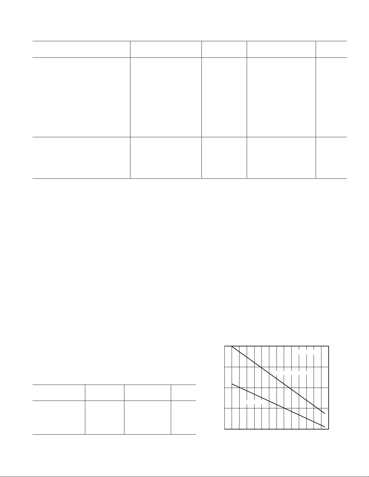
Fine-Scale Gain Flatness vs. Frequency, G = +2, RL= 150
REV. A
Information furnished by Analog Devices is believed to be accurate and
reliable. However, no responsibility is assumed by Analog Devices for its
use, nor for any infringements of patents or other rights of third parties
which may result from its use. No license is granted by implication or
otherwise under any patent or patent rights of Analog Devices.
Ω
Channel Switching Characteristics for a 3:1 Mux
© Analog Devices, Inc., 1995
One Technology Way, P.O. Box 9106, Norwood, MA 02062-9106, U.S.A.
Tel: 617/329-4700 Fax: 617/326-8703
Page 2

AD8013–SPECIFICA TIONS
(@ TA = +258C, R
= 150 V, unless otherwise noted)
LOAD
Model AD8013A
Conditions V
S
Min Typ Max Units
DYNAMIC PERFORMANCE
Bandwidth (3 dB) No Peaking, G = +2 +5 V 100 125 MHz
No Peaking, G = +2 ±5 V 110 140 MHz
Bandwidth (0.1 dB) No Peaking, G = +2 +5 V 50 MHz
No Peaking, G = +2 ±5 V 60 MHz
Slew Rate 2 V Step +5 V 400 V/µs
6 V Step ±5 V 600 1000 V/µs
Settling Time to 0.1% 0 V to +2 V ±5 V 18 ns
4.5 V Step, C
R
> 1 kΩ, RFB = 4 kΩ
LOAD
= 200 pF ±6 V 40 ns
LOAD
NOISE/HARMONIC PERFORMANCE
Total Harmonic Distortion f
= 5 MHz, RL = 1 k ±5 V –76 dBc
C
= 5 MHz, RL = 150 Ω±5 V –66 dBc
f
C
Input Voltage Noise f = 10 kHz +5 V, ±5 V 3.5 nV/√
Input Current Noise f = 10 kHz (–I
Differential Gain (R
Differential Phase (R
= 150 Ω) f = 3.58 MHz, G = +2 +5 V
L
= 150 Ω) f = 3.58 MHz, G = +2 +5 V
L
) +5 V, ±5 V 12 pA/√Hz
IN
1
±5 V 0.02 0.05 %
1
0.05 %
0.06 Degrees
±5 V 0.06 0.12 Degrees
DC PERFORMANCE
Input Offset Voltage T
MIN
to T
MAX
+5 V, ±5 V 2 5 mV
Offset Drift 7 µV/°C
Input Bias Current (–) +5 V, ± 5 V 2 10 µA
Input Bias Current (+) T
MIN
to T
MAX
+5 V, ±5 V 3 15 µA
Open-Loop Transresistance +5 V 650 800 kΩ
to T
T
MIN
MAX
550 kΩ
±5 V 800 k 1.1 M Ω
T
MIN
to T
MAX
650 kΩ
INPUT CHARACTERISTICS
Input Resistance +Input ±5 V 200 kΩ
–Input ±5 V 150 Ω
Input Capacitance ±5 V 2 pF
Input Common-Mode Voltage Range ±5 V 3.8 ±V
+5 V 1.2 3.8 +V
Common-Mode Rejection Ratio
Input Offset Voltage +5 V 52 56 dB
Input Offset Voltage ±5 V 52 56 dB
–Input Current +5 V, ±5 V 0.2 0.4 µA/V
+Input Current +5 V, ±5 V 5 7 µA/V
Hz
OUTPUT CHARACTERISTICS
Output Voltage Swing
RL = 1 kΩ VOL–V
V
= 150 Ω VOL–V
R
L
CC–VOH
V
CC–VOH
EE
EE
0.8 1.0 V
0.8 1.0 V
1.1 1.3 V
1.1 1.3 V
Output Current +5 V 30 mA
±5 V 25 30 mA
Short-Circuit Current ±5 V 95 mA
Capacitive Load Drive ±5 V 1000 pF
MATCHING CHARACTERISTICS
Dynamic
Crosstalk G = +2, f = 5 MHz +5 V, ±5 V 70 dB
Gain Flatness Match f = 20 MHz ±5 V 0.1 dB
DC
Input Offset Voltage +5 V, ± 5 V 0.3 mV
–Input Bias Current +5 V, ±5 V 1.0 µA
–2–
REV. A
Page 3
Model AD8013A
MAXIMUM POWER DISSIPATION – Watts
AMBIENT TEMPERATURE – °C
2.5
2.0
0.5
–50 90–40 –30 –20 0 10 20 30 40 50 60 70 80
1.5
1.0
–10
TJ = +150°C
14-PIN DIP PACKAGE
14-PIN SOIC
Conditions V
S
Min Typ Max Units
POWER SUPPLY
Operating Range Single Supply +4.2 +13 V
Dual Supply ±2.1 ±6.5 V
Quiescent Current/Amplifier +5 V 3.0 3.5 mA
± 5 V 3.4 4.0 mA
±6.5 V 3.5 mA
Quiescent Current/Amplifier Power Down +5 V 0.25 0.35 mA
± 5 V 0.3 0.4 mA
Power Supply Rejection Ratio
Input Offset Voltage V
= ±2.5 V to ±5 V 70 76 dB
S
–Input Current +5 V, ±5 V 0.03 0.2 µA/V
+Input Current +5 V, ±5 V 0.07 1.0 µA/V
DISABLE CHARACTERISTICS
Off Isolation f = 6 MHz +5 V, ±5 V –70 dB
Off Output Impedance G = +1 +5 V, ± 5 V 12 pF
Turn-On Time 50 ns
Turn-Off Time 30 ns
Switching Threshold –VS + xV 1.3 1.6 1.9 V
NOTES
1
The test circuit for differential gain and phase measurements on a +5 V supply is ac coupled.
Specifications subject to change without notice.
ABSOLUTE MAXIMUM RATINGS
Supply Voltage . . . . . . . . . . . . . . . . . . . . . . . . . . 13.2 V Total
Internal Power Dissipation
2
1
Plastic (N) . . . . . . . . . 1.6 Watts (Observe Derating Curves)
Small Outline (R) . . . . 1.0 Watts (Observe Derating Curves)
Input Voltage (Common Mode) . . Lower of ±V
or ±12.25 V
S
Differential Input Voltage . . . . . . . . Output ±6 V (Clamped)
Output Voltage Limit
Maximum . . . . . . . . . Lower of (+12 V from –V
Minimum . . . . . . . . . Higher of (–12.5 V from +V
) or (+VS)
S
) or (–VS)
S
Output Short Circuit Duration
. . . . . . . . . . . . . . . . . . . .Observe Power Derating Curves
Storage Temperature Range
N and R Package . . . . . . . . . . . . . . . . . . . –65°C to +125°C
Operating Temperature Range
AD8013A . . . . . . . . . . . . . . . . . . . . . . . . . . –40°C to +85°C
Lead Temperature Range (Soldering 10 sec) . . . . . . . .+300°C
NOTES
1
Stresses above those listed under “Absolute Maximum Ratings” may cause
permanent damage to the device. This is a stress rating only and functional
operation of the device at these or any other conditions above those indicated in
the operational section of this specification is not implied. Exposure to absolute
maximum rating conditions for extended periods may affect device reliability.
2
Specification is for device in free air:
14-Pin Plastic DIP Package: θJA = 75°C/Watt
14-Pin SOIC Package: θJA = 120°C/Watt
Maximum Power Dissipation
The maximum power that can be safely dissipated by the AD8013
is limited by the associated rise in junction temperature. The
maximum safe junction temperature for the plastic encapsulated
parts is determined by the glass transition temperature of the
plastic, about 150°C. Exceeding this limit temporarily may
cause a shift in parametric performance due to a change in the
stresses exerted on the die by the package. Exceeding a junction
temperature of 175°C for an extended period can result in
device failure.
While the AD8013 is internally short circuit protected, this may
not be enough to guarantee that the maximum junction temperature is not exceeded under all conditions. To ensure proper
operation, it is important to observe the derating curves.
It must also be noted that in (noninverting) gain configurations
(with low values of gain resistor), a high level of input overdrive
can result in a large input error current, which may result in a
significant power dissipation in the input stage. This power
must be included when computing the junction temperature rise
due to total internal power.
AD8013
Model Range Description Options
AD8013AN –40°C to +85°C 14-Pin Plastic DIP N-14
AD8013AR-14 –40°C to +85°C 14-Pin Plastic SOIC R-14
AD8013AR-14-REEL –40°C to +85°C 14-Pin Plastic SOIC R-14
AD8013AR-14-REEL7 –40°C to +85°C 14-Pin Plastic SOIC R-14
AD8013ACHIPS –40°C to +85°C Die Form
REV. A
ORDERING GUIDE
Temperature Package Package
Maximum Power Dissipation vs. Ambient Temperature
–3–
Page 4
AD8013
METALIZATION PHOTO
Contact factory for latest dimensions.
Dimensions shown in inches and (mm).
+v
4
DISABLE 3
s
3
10
+IN3
0.071 (1.81)
11
–V
S
12
+IN2
13
–IN2
–IN1 6
OUT1 7
0.044 (1.13)
OUT3 8
–IN3 9
+IN1
5
CAUTION
ESD (electrostatic discharge) sensitive device. Electrostatic charges as high as 4000 V readily
accumulate on the human body and test equipment and can discharge without detection. Although
the AD8013 features proprietary ESD protection circuitry, permanent damage may occur on devices
subjected to high energy electrostatic discharges. Therefore, proper ESD precautions are recommended to avoid performance degradation or loss of functionality.
2 DISABLE 2
1 DISABLE 1
14 OUT 2
WARNING!
ESD SENSITIVE DEVICE
6
5
4
3
2
1
COMMON-MODE VOLTAGE RANGE – ± Volts
0
172
3456
SUPPLY VOLTAGE – ± Volts
Figure 1. Input Common-Mode Voltage Range vs.
Supply Voltage
12
10
8
6
4
OUTPUT VOLTAGE SWING – V p-p
2
0
172
3456
SUPPLY VOLTAGE – ± Volts
NO LOAD
RL = 150Ω
Figure 2. Output Voltage Swing vs. Supply Voltage
–4–
REV. A
Page 5

AD8013
JUNCTION TEMPERATURE – °C
3
0
–3
–60 140–40
INPUT BIAS CURRENT – µA
–20 0 20 40 60 80 100 120
2
1
–1
–2
–I
B
+I
B
JUNCTION TEMPERATURE – °C
2
–1
–4
–60 140–40
INPUT OFFSET VOLTAGE – mV
–20 0 20 40 60 80 100 120
1
0
–2
–3
VS = +5V
VS = ±5V
JUNCTION TEMPERATURE – °C
140
130
80
–60 140–40
SHORT CIRCUIT CURRENT – mA
–20 0 20 40 60 80 100 120
120
100
90
SOURCE
SINK
VS = ± 5V
10
8
6
4
2
OUTPUT VOLTAGE SWING – V p-p
0
10 10k100
VS = ±5V
VS = +5V
LOAD RESISTANCE – Ω
1k
Figure 3. Output Voltage Swing vs. Load Resistance
12
11
VS = ± 5V
10
9
8
SUPPLY CURRENT – mA
7
VS = +5V
Figure 6. Input Bias Current vs. Junction Temperature
Figure 4. Total Supply Current vs. Junction Temperature
REV. A
Figure 5. Supply Current vs. Supply Voltage
6
–60 140–40
11
10
9
SUPPLY CURRENT – mA
8
7
1723456
–20 0 20 40 60 80 100 120
JUNCTION TEMPERATURE – °C
TA = +25°C
SUPPLY VOLTAGE – ± Volts
Figure 7. Input Offset Voltage vs. Junction
Temperature
Figure 8. Short Circuit Current vs. Junction
Temperature
–5–
Page 6

AD8013
FREQUENCY – Hz
10
100k 1G1M
COMMON-MODE REJECTION – dB
10M 100M
70
60
20
50
40
30
V
CM
R
R
R
R
1k
100
10
G = +2
1
0.1
CLOSED-LOOP OUTPUT RESISTANCE – Ω
0.01
100k 1G1M
VS = ±5V
FREQUENCY – Hz
10M 100M
Figure 9. Closed-Loop Output Resistance vs.
Frequency
100k
10k
1k
OUTPUT RESISTANCE – Ω
100
10
1M 1G10M
FREQUENCY – Hz
100M
Figure 12. Common-Mode Rejection vs. Frequency
80
70
60
50
40
30
20
POWER SUPPLY REJECTION – dB
10
0
100k 1G1M 10M 100M
+PSR
–PSR
FREQUENCY – Hz
VS = ±5V
Figure 10. Output Resistance vs. Frequency, Disabled
State
1k
Hz
√
100
10
VOLTAGE NOISE nV/
1
100 1M1k
Figure 11. Input Current and Voltage Noise vs.
Frequency
V
NOISE
FREQUENCY – Hz
NONINVERTING I
INVERTING I
10k 100k
1k
Hz
√
100
10
CURRENT NOISE pA/
1
Figure 13. Power Supply Rejection Ratio vs. Frequency
140
120
100
80
TRANSIMPEDANCE – dB
60
40
10k
100k 1G1M
FREQUENCY – Hz
10M 100M
VS = ±5V
R
L
= 1k
0
–45
–90
–135
PHASE – Degrees
–180
Figure 14. Open-Loop Transimpedance vs. Frequency
Ω
(Relative to 1
)
–6–
REV. A
Page 7

–30
FREQUENCY – Hz
1M 1G10M
CLOSED-LOOP GAIN
(NORMALIZED) – dB
100M
–6
+1
0
–1
–2
–3
–4
–5
0
–90
–180
–270
PHASE SHIFT – Degrees
G = +1
R
L
= 150Ω
VS = ±5V
VS = +5V
VS = +5V
VS = ±5V
GAIN
PHASE
10
0%
100
90
20ns
500mV
500mV
V
IN
V
OUT
G = +2
–40
= 2V p-p
V
O
V
= ±5V
S
–50
–60
–70
2nd
–80
R
= 150Ω
L
–90
–100
2nd
HARMONIC DISTORTION – dBc
R
= 1kΩ
L
–110
–120
1k 100M10k
3rd
R
= 150Ω
L
3rd
R
= 1kΩ
L
100k 1M 10M
FREQUENCY – Hz
AD8013
Figure 15. Harmonic Distortion vs. Frequency
1800
1600
1400
1200
1000
SLEW RATE – V/µs
VS = ±5V
R
= 500Ω
L
800
600
400
200
18234567
OUTPUT STEP SIZE – V p-p
G = +10
G = –1
G = +2
G = +1
Figure 16. Slew Rate vs. Output Step Size
2V
100
90
V
IN
20ns
Figure 18. Closed-Loop Gain and Phase vs. Frequency,
= 150
G = +1, R
2000
1800
1600
1400
1200
1000
800
SLEW RATE – V/µs
600
400
200
L
1.5 7.52.5
Ω
G = +10
3.5 4.5 5.5 6.5
SUPPLY VOLTAGE – ±Volts
G = –1
G = +2
G = +1
Figure 19. Maximum Slew Rate vs. Supply Voltage
V
10
OUT
0%
2V
Figure 17. Large Signal Pulse Response, Gain = +1,
(R
= 2 kΩ, RL = 150 Ω, VS = ±5 V)
F
REV. A
Figure 20. Small Signal Pulse Response, Gain = +1,
(RF = 2 kΩ, RL = 150 Ω, VS = ±5 V)
–7–
Page 8

AD8013
10
0%
100
90
20ns2V
2V
V
IN
V
OUT
10
0%
100
90
20ns
500mV
500mV
V
IN
V
OUT
V
V
OUT
20ns50mV
100
90
IN
10
0%
500mV
Figure 21. Large Signal Pulse Response, Gain = +10,
R
= 301 Ω, RL = 150 Ω, VS = ±5 V)
F
G = +10
R
PHASE
+1
0
GAIN
–1
–2
–3
–4
(NORMALIZED) – dB
CLOSED-LOOP GAIN
–5
–6
1M 1G10M
VS = +5V
VS = ±5V
FREQUENCY – Hz
VS = +5V
100M
= 150Ω
L
VS = ±5V
0
–90
–180
–270
PHASE SHIFT – Degrees
Figure 22. Closed-Loop Gain and Phase vs. Frequency,
G = +10, RL = 150
100
V
90
IN
50mV
Ω
20ns
Figure 24. Large Signal Pulse Response, Gain = –1,
(RF = 698 Ω, RL = 150 Ω, VS = ±5 V)
PHASE
+1
0
GAIN
–1
–2
–3
–4
(NORMALIZED) – dB
CLOSED-LOOP GAIN
–5
–6
1M 1G10M
VS = +5V
VS = +5V
FREQUENCY – Hz
100M
G = –1
= 150Ω
R
L
VS = ±5V
VS = ±5V
180
90
0
–90
PHASE SHIFT – Degrees
Figure 25. Closed-Loop Gain and Phase vs. Frequency,
G = –1, RL = 150
Ω
V
10
OUT
0%
500mV
Figure 23. Small Signal Pulse Response, Gain = +10,
= 301 Ω, RL = 150 Ω, VS = ±5 V)
(R
F
Figure 26. Small Signal Pulse Response, Gain = –1,
(R
= 698 Ω, RL = 150 Ω, VS = ±5 V)
F
–8–
REV. A
Page 9

G = –10
1
2 π C
T(RF
+Gn rin)
R
PHASE
+1
0
GAIN
–1
–2
–3
–4
(NORMALIZED) – dB
CLOSED-LOOP GAIN
–5
–6
1M 1G10M
VS = +5V
VS = +5V
FREQUENCY – Hz
100M
L
VS = ±5V
VS = ±5V
= 150Ω
180
90
0
–90
PHASE SHIFT – Degrees
Figure 27. Closed-Loop Gain and Phase vs. Frequency,
G = –10, R
= 150
L
Ω
General
The AD8013 is a wide bandwidth, triple video amplifier that
offers a high level of performance on less than 4.0 mA per
amplifier of quiescent supply current. The AD8013 uses a
proprietary enhancement of a conventional current feedback
architecture, and achieves bandwidth in excess of 200MHz with
low differential gain and phase errors, making it an extremely
efficient video amplifier.
The AD8013’s wide phase margin coupled with a high output
short circuit current make it an excellent choice when driving
any capacitive load. High open-loop gain and low inverting
input bias current enable it to be used with large values of
feedback resistor with very low closed-loop gain errors.
It is designed to offer outstanding functionality and performance
at closed-loop inverting or noninverting gains of one or greater.
Choice of Feedback & Gain Resistors
Because it is a current feedback amplifier, the closed-loop bandwidth of the AD8013 may be customized using different values
of the feedback resistor. Table I shows typical bandwidths at
different supply voltages for some useful closed-loop gains when
driving a load of 150 Ω.
The choice of feedback resistor is not critical unless it is
important to maintain the widest, flattest frequency response.
The resistors recommended in the table are those (chip
resistors) that will result in the widest 0.1 dB bandwidth without
peaking. In applications requiring the best control of bandwidth,
1% resistors are adequate. Package parasitics vary between the
14-pin plastic DIP and the 14-pin plastic SOIC, and may result
in a slight difference in the value of the feedback resistor used to
achieve the optimum dynamic performance. Resistor values and
widest bandwidth figures are shown in parenthesis for the SOIC
where they differ from those of the DIP. Wider bandwidths than
those in the table can be attained by reducing the magnitude of
the feedback resistor (at the expense of increased peaking),
while peaking can be reduced by increasing the magnitude of
the feedback resistor.
Increasing the feedback resistor is especially useful when driving
large capacitive loads as it will increase the phase margin of the
closed-loop circuit. (Refer to the section on driving capacitive
loads for more information.)
AD8013
To estimate the –3 dB bandwidth for closed-loop gains of 2 or
greater, for feedback resistors not listed in the following table,
the following single pole model for the AD8013 may be used:
ACL .
1+ SC
where: CT = transcapacitance > 1 pF
R
= feedback resistor
F
G = ideal closed loop gain
Gn =
rin = inverting input resistance > 150 Ω
1+
R
F
= noise gain
R
G
ACL = closed loop gain
The –3 dB bandwidth is determined from this model as:
.
f
3
This model will predict –3 dB bandwidth to within about 10%
to 15% of the correct value when the load is 150 Ω and V
±5 V. For lower supply voltages there will be a slight decrease in
bandwidth. The model is not accurate enough to predict either
the phase behavior or the frequency response peaking of the
AD8013.
It should be noted that the bandwidth is affected by attenuation
due to the finite input resistance. Also, the open-loop output
resistance of about 12 Ω reduces the bandwidth somewhat when
driving load resistors less than about 250 Ω. (Bandwidths will
be about 10% greater for load resistances above a few hundred
ohms.)
Table I. –3 dB Bandwidth vs. Closed-Loop Gain and Feedback
Resistor, R
= 150 Ω (SOIC)
L
VS – Volts Gain RF – Ohms BW – MHz
±5 +1 2000 230
+2 845 (931) 150 (135)
+10 301 80
–1 698 (825) 140 (130)
–10 499 85
+5 +1 2000 180
+2 887 (931) 120 (130)
+10 301 75
–1 698 (825) 130 (120)
–10 499 80
Driving Capacitive Loads
When used in combination with the appropriate feedback
resistor, the AD8013 will drive any load capacitance without
oscillation. The general rule for current feedback amplifiers is
that the higher the load capacitance, the higher the feedback
resistor required for stable operation. Due to the high open-loop
transresistance and low inverting input current of the AD8013,
the use of a large feedback resistor does not result in large closedloop gain errors. Additionally, its high output short circuit current
makes possible rapid voltage slewing on large load capacitors.
For the best combination of wide bandwidth and clean pulse
response, a small output series resistor is also recommended.
Table II contains values of feedback and series resistors which
result in the best pulse responses. Figure 29 shows the AD8013
driving a 300 pF capacitor through a large voltage step with
virtually no overshoot. (In this case, the large and small signal
pulse responses are quite similar in appearance.)
T(RF
G
+Gn rin)
=
S
REV. A
–9–
Page 10

AD8013
75Ω
75Ω
V
OUT
75Ω
CABLE
75Ω
75Ω
CABLE
4
+V
S
AD8013
0.1µF
11
0.1µF
–V
S
R
G
V
IN
R
F
R
F
1.0µF
+V
S
R
G
V
IN
R
T
Figure 28. Circuit for Driving a Capacitive Load
Table II. Recommended Feedback and Series Resistors vs.
Capacitive Load and Gain
CL – pF RF – Ohms G = 2 G ≥ 3
20 2k 25 15
50 2k 25 15
100 3k 20 15
200 4k 15 15
300 6k 15 15
≥500 7k 15 15
500mV
100
90
V
IN
10
V
OUT
0%
1V
Figure 29. Pulse Response Driving a Large Load Capacitor.
= 300 pF, G = +2, RF = 6k, RS = 15
C
L
Overload Recovery
The three important overload conditions are: input commonmode voltage overdrive, output voltage overdrive, and input
current overdrive. When configured for a low closed-loop gain,
the amplifier will quickly recover from an input commonmode voltage overdrive; typically in under 25 ns. When configured for a higher gain, and overloaded at the output, the
recovery time will also be short. For example, in a gain of +10,
with 15% overdrive, the recovery time of the AD8013 is about
20 ns (see Figure 30). For higher overdrive, the response is
somewhat slower. For 6 dB overdrive, (in a gain of +10), the
recovery time is about 65 ns.
500mV
100
90
V
IN
4
AD8013
11
–V
0.1µF
15Ω
1.0µF
0.1µF
S
R
S
V
O
C
L
RS – Ohms
50ns
Ω
50ns
As noted in the warning under “Maximum Power Dissipation,”
a high level of input overdrive in a high noninverting gain circuit
can result in a large current flow in the input stage. Though this
current is internally limited to about 30 mA, its effect on the
total power dissipation may be significant.
High Performance Video Line Driver
At a gain of +2, the AD8013 makes an excellent driver for a
back terminated 75 Ω video line (Figures 31, 32, and 33). Low
differential gain and phase errors and wide 0.1 dB bandwidth
can be realized. The low gain and group delay matching errors
ensure excellent performance in RGB systems. Figures 34 and
35 show the worst case matching.
Figure 31. A Video Line Driver Operating at a Gain of +2
= RG from Table I)
(R
F
G = +2
R
PHASE
+1
0
GAIN
–1
–2
–3
–4
(NORMALIZED) – dB
CLOSED-LOOP GAIN
–5
–6
1M 1G10M
VS = +5V
VS = +5V
FREQUENCY – Hz
100M
= 150Ω
L
VS = ±5V
VS = ±5V
0
–90
–180
–270
PHASE SHIFT – Degrees
Figure 32. Closed-Loop Gain & Phase vs. Frequency
for the Line Driver
G = +2
R
= 150Ω
+0.2
+0.1
0
–0.1
–0.2
–0.3
–0.4
NORMALIZED GAIN – dB
–0.5
VS = +5V
L
VS = ±5V
10
V
OUT
0%
Figure 30. 15% Overload Recovery, G = +10 (RF = 300 Ω,
= 1 kΩ, VS = ±5 V)
R
L
5V
Figure 33. Fine-Scale Gain Flatness vs. Frequency,
G = +2, R
–10–
1M 1G10M
= 150
L
Ω
FREQUENCY – Hz
100M
REV. A
Page 11

1.5
+5V
10k
TO DISABLE PIN
V
I
VI HIGH => AMPLIFIER ENABLED
V
I
LOW => AMPLIFIER DISABLED
–5V
4k
8k
10
0%
100
90
200ns
500mV
5V
1.0
0.5
G = +2
RL = 150Ω
AD8013
0
–0.5
GAIN MATCHING – dB
–1.0
–1.5
VS = ±5V
VS = +5V
Figure 36. Level Shifting to Drive Disable Pins on Dual
Supplies
The AD8013’s input stages include protection from the large
–2.0
1M 1G10M
FREQUENCY – Hz
100M
differential input voltages that may be applied when disabled.
Internal clamps limit this voltage to about ±3 V. The high input to
output isolation will be maintained for voltages below this limit.
Figure 34. Closed-Loop Gain Matching vs. Frequency
10
G = +2
8
RL = 150Ω
6
VS = ±5V
VS = +5V
FREQUENCY – Hz
DELAY
DELAY
MATCHING
VS = ±5V
VS = +5V
10M
4
2
1.0
G = +2
0.5
RL = 150Ω
GROUP DELAY – ns
0
–0.5
–1.0
100k 100M1M
Figure 35. Group Delay and Group Delay Matching
vs. Frequency, G = +2, R
= 150
L
Ω
Disable Mode Operation
Pulling the voltage on any one of the Disable pins about 1.6V
up from the negative supply will put the corresponding
amplifier into a disabled, powered down, state. In this
condition, the amplifier’s quiescent current drops to about
0.3 mA, its output becomes a high impedance, and there is
a high level of isolation from input to output. In the case of
the gain of two line driver for example, the impedance at the
output node will be about the same as for a 1.6 kΩ resistor
(the feedback plus gain resistors) in parallel with a 12 pF
capacitor and the input to output isolation will be about
3:1 Video Multiplexer
Wiring the amplifier outputs together will form a 3:1 mux with
excellent switching behavior. Figure 37 shows a recommended
configuration which results in –0.1 dB bandwidth of 35 MHz
and OFF channel isolation of 60 dB at 10 MHz on ± 5 V
supplies. The time to switch between channels is about 50 ns.
Switching time is virtually unaffected by signal level.
665Ω
845Ω
+V
S
V
DISABLE 1
V
DISABLE 2
V
DISABLE 3
654
13
12 2
9
10
1
845Ω
845Ω
3
1
IN
IN
IN
75Ω
665Ω
2
75Ω
665Ω
3
75Ω
84Ω
7
75Ω
CABLE
84Ω
14
84Ω
8
11
–V
S
75Ω
V
OUT
66 dB at 5 MHz.
Leaving the Disable pin disconnected (floating) will leave
the corresponding amplifier operational, in the enabled
Figure 37. A Fast Switching 3:1 Video Mux (Supply
Bypassing Not Shown)
state. The input impedance of the disable pin is about 40 kΩ
in parallel with a few picofarads. When driven to 0 V, with
the negative supply at –5 V, about 100 µA flows into the
disable pin.
When the disable pins are driven by complementary output
CMOS logic, on a single 5 V supply, the disable and enable
times are about 50 ns. When operated on dual supplies,
level shifting will be required from standard logic outputs to
the Disable pins. Figure 36 shows one possible method
which results in a negligible increase in switching time.
REV. A
Figure 38. Channel Switching Characteristic for the
3:1 Mux
–11–
Page 12

AD8013
2:1 Video Multiplexer
Configuring two amplifiers as unity gain followers and using the
third to set the gain results in a high performance 2:1 mux
(Figures 39 and 40). This circuit takes advantage of the very low
crosstalk between Channels 2 and 3 to achieve the OFF channel
isolation shown in Figure 40. This circuit can achieve
differential gain and phase of 0.03% and 0.07° respectively.
R1
2kΩ
R3
10Ω
R4
10Ω
8
R2
2kΩ
R6
845Ω
5
6
7
1
R5
845Ω
V
OUT
VINA
VINB
13
14
2
12
2
DISABLE
10
3
9
3
DISABLE
Figure 39. 2:1 Mux with High Isolation and Low
Differential Gain and Phase Errors
2
1
0
–1
–2
–3
–4
–5
CLOSED-LOOP GAIN – dB
–6
–7
–8
FEEDTHROUGH
10M
FREQUENCY – Hz
100M
GAIN
–30
–40
–50
–60
–70
–80
1G1M
FEEDTHROUGH – dB
The AD8013 can be used to build a circuit for switching between
any two arbitrary gains while maintaining a constant input
impedance. The example of Figure 41 shows a circuit for switching
between a noninverting gain of 1 and an inverting gain of 1. The
total time for channel switching and output voltage settling is
about 80 ns.
698Ω 698Ω
+5V
845Ω
10
6
5
9
845Ω
DIS 1
DIS 3
–5V
4
7
1
15Ω
V
OUT
3
8
11
2k
13
100Ω
V
IN
50Ω
14
12
1k
1k
Figure 41. Circuit to Switch Between Gains of –1 and +1
500mV5V500mV
100
90
10
0%
200ns
Figure 42. Switching Characteristic for Circuit of Figure 41
C2084–18–10/95
Figure 40. 2:1 Mux ON Channel Gain and Mux OFF Channel
Feedthrough vs. Frequency
Gain Switching
OUTLINE DIMENSIONS
Dimensions shown in inches and (mm).
14-Lead Plastic DIP (N-14)
0.795 (20.19)
0.725 (18.42)
0.210 (5.33)
MAX
0.160 (4.06)
0.115 (2.93)
14
17
PIN 1
0.022 (0.558)
0.014 (0.356)
0.100
(2.54)
BSC
8
0.280 (7.11)
0.240 (6.10)
0.060 (1.52)
0.015 (0.38)
0.070 (1.77)
0.045 (1.15)
0.130
(3.30)
MIN
SEATING
PLANE
0.325 (8.25)
0.300 (7.62)
0.015 (0.381)
0.008 (0.204)
0.195 (4.95)
0.115 (2.93)
–12–
0.1574 (4.00)
0.1497 (3.80)
0.0098 (0.25)
0.0040 (0.10)
SEATING
PLANE
14-Lead SOIC (R-14)
0.3444 (8.75)
0.3367 (8.55)
14 8
PIN 1
0.0500
0.0192 (0.49)
(1.27)
0.0138 (0.35)
BSC
0.2440 (6.20)
71
0.2284 (5.80)
0.0688 (1.75)
0.0532 (1.35)
0.0098 (0.25)
0.0075 (0.19)
0.0196 (0.50)
0.0099 (0.25)
8°
0°
0.0500 (1.27)
0.0160 (0.41)
PRINTED IN U.S.A.
x 45°
REV. A
 Loading...