

Datasheet AD8012ARM-REEL7, AD8012ARM-REEL, AD8012ARM, AD8012AR-REEL7, AD8012AR-REEL Datasheet (Analog Devices)
...Page 1
Dual 350 MHz
AMP 1
V
IN
V
REF
R2
R1
RL = 100V
OR
135V
V
OUT
Np:Ns
TRANSFORMER
LINE
POWER
IN dB
+V
S
+
–
–V
S
+
–
a
FEATURES
Low Power
1.7 mA/Amplifier Supply Current
Fully Specified for ⴞ5 V and +5 V Supplies
High Output Current, 125 mA
High Speed
350 MHz, –3 dB Bandwidth (G = +1)
150 MHz, –3 dB Bandwidth (G = +2)
2,250 V/s Slew Rate
20 ns Settling Time to 0.1%
Low Distortion
–72 dBc Worst Harmonic @ 500 kHz, R
–66 dBc Worst Harmonic @ 5 MHz, R
Good Video Specifications (R
= 1 k⍀, G = +2)
L
0.02% Differential Gain Error
0.06ⴗ Differential Phase Error
Gain Flatness 0.1 dB to 40 MHz
60 ns Overdrive Recovery
Low Offset Voltage, 1.5 mV
Low Voltage Noise, 2.5 nV/√Hz
Available in 8-Lead SOIC and 8-Lead microSOIC
APPLICATIONS
XDSL, HDSL Line Driver
ADC Buffer
Professional Cameras
CCD Imaging System
Ultrasound Equipment
Digital Camera
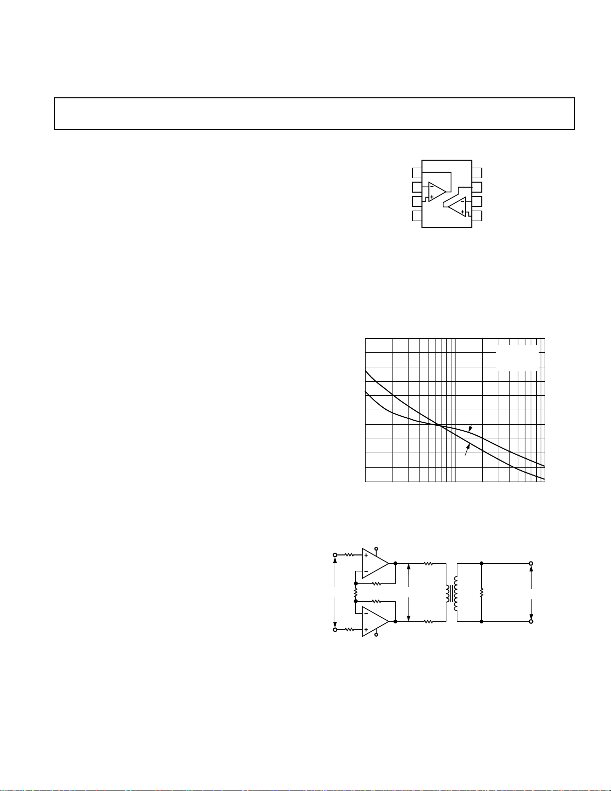
PRODUCT DESCRIPTION
The AD8012 is a dual low power current feedback amplifier
capable of providing 350 MHz bandwidth while using only
1.7 mA per amplifier. It is intended for use in high frequency,
wide dynamic range systems where low distortion, high speed
are essential and low power is critical.
With only 1.7 mA of supply current, the AD8012 also offers
exceptional ac specs such as 20 ns settling time and 2,250 V/µs
slew rate. The video specifications are 0.02% differential gain
and 0.06 degree differential phase, excellent for such a low power
amplifier. In addition, the AD8012 has a low offset of 1.5 mV.
The AD8012 is well suited for any application that requires high
performance with minimal power.
The product is available in standard 8-lead SOIC or microSOIC packages and operates over the industrial temperature
range –40°C to +85°C.
= 100 ⍀
L
= 1 k⍀
L
Low Power Amplifier
AD8012
FUNCTIONAL BLOCK DIAGRAM
+V
2nd
3rd
8
S
OUT2
7
6
–IN2
+IN2–V
5
G = +2
= 2V p-p
V
OUT
R
= 750V
F
OUT1
1
2
–IN1
3
+IN1
4
S
AD8012
–40
–50
–60
–70
DISTORTION – dBc
–80
–90
10 1k100
RL – V
Figure 1. Distortion vs. Load Resistance, VS = ±5 V,
Frequency = 500 kHz
Figure 2. Differential Drive Circuit for XDSL Applications
*
*Protected under U.S. Patent Number 5,537,079.
REV. A
Information furnished by Analog Devices is believed to be accurate and
reliable. However, no responsibility is assumed by Analog Devices for its
use, nor for any infringements of patents or other rights of third parties
which may result from its use. No license is granted by implication or
otherwise under any patent or patent rights of Analog Devices.
One Technology Way, P.O. Box 9106, Norwood, MA 02062-9106, U.S.A.
Tel: 781/329-4700 World Wide Web Site: http://www.analog.com
Fax: 781/326-8703 © Analog Devices, Inc., 1999
Page 2

AD8012–SPECIFICATIONS
DUAL SUPPLY
(@ TA = +25ⴗC, VS = ⴞ5 V, G = +2, RL = 100 ⍀, RF = RG = 750 ⍀, unless otherwise noted)
Parameter Conditions Min Typ Max Units
DYNAMIC PERFORMANCE
–3 dB Small Signal Bandwidth G = +1, V
G␣ =␣ +2, V
G␣ =␣ +2, V
0.1 dB Bandwidth V
Large Signal Bandwidth V
Slew Rate V
Rise and Fall Time V
< 0.4 V p-p, R
OUT
= 4 V p-p 75 MHz
OUT
= 4 V p-p 2,250 V/µs
OUT
= 2 V p-p 3 ns
OUT
Settling Time 0.1%, V
0.02%, V
< 0.4 V p-p, R
OUT
< 0.4 V p-p, R
OUT
< 0.4 V p-p, R
OUT
= 2 V p-p 20 ns
OUT
= 2 V p-p 35 ns
OUT
= 1 kΩ/100 Ω 40/23 MHz
L
= 1 kΩ 270 350 MHz
L
= 1 kΩ 95 150 MHz
L
= 100 Ω 90 MHz
L
Overdrive Recovery 2× Overdrive 60 ns
NOISE/HARMONIC PERFORMANCE
Distortion V
2nd Harmonic 500 kHz, R
3rd Harmonic 500 kHz, R
Output IP3 500 kHz, ∆f = 10 kHz, R
IMD 500 kHz, ∆f = 10 kHz, R
Crosstalk 5 MHz, R
= 2 V p-p, G = +2
OUT
5 MHz, R
5 MHz, R
= 1 kΩ/100 Ω –89/–73 dBc
L
= 1 kΩ/100 Ω –78/–62 dBc
L
= 1 kΩ/100 Ω –84/–72 dBc
L
= 1 kΩ/100 Ω –66/–52 dBc
L
= 100 Ω –70 dB
L
= 1 kΩ/100 Ω 30/40 dBm
L
= 1 kΩ/100 Ω –79/–77 dBc
L
Input Voltage Noise f = 10 kHz 2.5 nV/√Hz
Input Current Noise f = 10 kHz,␣ +Input, –Input 15 pA/√Hz
Differential Gain f = 3.58 MHz, R
Differential Phase f = 3.58 MHz, R
= 150 Ω/1 kΩ, G = +2 0.02/0.02 %
L
= 150 Ω/1 kΩ, G = +2 0.3/0.06 Degrees
L
DC PERFORMANCE
Input Offset Voltage ±1.5 ±4mV
Open-Loop Transimpedance V
T
MIN–TMAX
= ±2 V, RL = 100 Ω 240 500 kΩ
OUT
T
MIN–TMAX
200 kΩ
±5mV
INPUT CHARACTERISTICS
Input Resistance +Input 450 kΩ
Input Capacitance +Input 2.3 pF
Input Bias Current +Input, –Input ±3 ±12 µA
Common-Mode Rejection Ratio V
+Input, –Input, T
= ±2.5 V –56 –60 dB
CM
MIN–TMAX
±15 µA
Input Common-Mode Voltage Range ±3.8 ±4.1 V
OUTPUT CHARACTERISTICS
Output Resistance G = +2 0.1 Ω
Output Voltage Swing ±3.85 ±4V
Output Current T
MIN–TMAX
70 125 mA
Short Circuit Current 500 mA
POWER SUPPLY
Supply Current/Amp 1.7 1.8 mA
T
MIN–TMAX
1.9 mA
Operating Range Dual Supply ±1.5 ±6.0 V
Power Supply Rejection Ratio –58 –60 dB
Specifications subject to change without notice.
–2– REV. A
Page 3

AD8012
SINGLE SUPPLY
(@ TA +25ⴗC, VS = +5 V, G = +2, RL = 100 ⍀, RF = RG = 750 ⍀, unless otherwise noted)
Parameter Conditions Min Typ Max Units
DYNAMIC PERFORMANCE
–3 dB Small Signal Bandwidth G = +1, V
G␣ =␣ +2, V
G␣ =␣ +2, V
0.1 dB Bandwidth V
Large Signal Bandwidth V
Slew Rate V
Rise and Fall Time V
< 0.4 V p-p, R
OUT
= 2 V p-p 60 MHz
OUT
= 3 V p-p 1,200 V/µs
OUT
= 2 V p-p 2 ns
OUT
Settling Time 0.1%, V
0.02%, V
< 0.4 V p-p, R
OUT
< 0.4 V p-p, R
OUT
< 0.4 V p-p, R
OUT
= 2 V p-p 25 ns
OUT
= 2 V p-p 40 ns
OUT
= 1 kΩ/100 Ω 43/24 MHz
L
= 1 kΩ 220 300 MHz
L
= 1 kΩ 90 140 MHz
L
= 100 Ω 85 MHz
L
Overdrive Recovery 2× Overdrive 60 ns
NOISE/HARMONIC PERFORMANCE
Distortion V
2nd Harmonic 500 kHz, R
3rd Harmonic 500 kHz, R
Output IP3 500 kHz, R
IMD 500 kHz, R
Crosstalk 5 MHz, R
= 2 V p-p, G = +2
OUT
5 MHz, R
5 MHz, R
= 1 kΩ/100 Ω –87/–71 dBc
L
= 1 kΩ/100 Ω –77/–61 dBc
L
= 1 kΩ/100 Ω –89/–72 dBc
L
= 1 kΩ/100 Ω –78/–52 dBc
L
= 1 kΩ/100 Ω 30/40 dBm
L
= 1 kΩ/100 Ω –77/–80 dBc
L
= 100 Ω –70 dB
L
Input Voltage Noise f = 10 kHz 2.5 nV/√Hz
Input Current Noise f = 10 kHz,␣ +Input, –Input 15 pA/√Hz
Black Level Clamped to +2 V, f = 3.58 MHz
Differential Gain R
Differential Phase R
= 150 Ω/1 kΩ 0.03/0.03 %
L
= 150 Ω/1 kΩ 0.4/0.08 Degrees
L
DC PERFORMANCE
Input Offset Voltage ±1 ±3mV
±4mV
Open-Loop Transimpedance V
T
MIN–TMAX
= 2 V p-p, R
OUT
T
MIN–TMAX
= 100 Ω 200 400 kΩ
L
150 kΩ
INPUT CHARACTERISTICS
Input Resistance +Input 450 kΩ
Input Capacitance +Input 2.3 pF
Input Bias Current +Input, –Input ±3 ±12 µA
Common-Mode Rejection Ratio V
+Input, –Input, T
= 1.5 V to 3.5 V –56 –60 dB
CM
MIN–TMAX
±15 µA
Input Common-Mode Voltage Range 1.5 to 3.5 1.2 to 3.8 V
OUTPUT CHARACTERISTICS
Output Resistance G = +2 0.1 Ω
Output Voltage Swing 1 to 4 0.9 to 4.2 V
Output Current T
MIN–TMAX
50 100 mA
Short Circuit Current 500 mA
POWER SUPPLY
Supply Current/Amp 1.55 1.75 mA
T
MIN–TMAX
1.85 mA
Operating Range Single Supply 3 12 V
Power Supply Rejection Ratio –58 –60 dB
Specifications subject to change without notice.
–3–REV. A
Page 4
AD8012
WARNING!
ESD SENSITIVE DEVICE
ABSOLUTE MAXIMUM RATINGS
Supply␣ Voltage . . . . . . . . . . . . . . . . . . . . . . . . . . . . . . . 12.6␣ V
Internal␣ Power␣ Dissipation
2
1
Small␣ Outline␣ Package (R) . . . . . . . . . . . . . . . . . . . . . 0.8␣ W
microSOIC Package (RM) . . . . . . . . . . . . . . . . . . . . . 0.6 W
Input Voltage (Common Mode) . . . . . . . . . . . . . . . . . . . ±V
S
Differential␣ Input␣ Voltage . . . . . . . . . . . . . . . . . . . . . . ±2.5␣ V
Output Short Circuit Duration
␣ ␣ . . . . . . . . . . . . . . . . . . . . . . Observe Power Derating Curves
Storage Temperature Range RM, R . . . . . . –65°C to +125°C
Operating Temperature Range (A Grade) . . –40°C to +85°C
Lead Temperature Range (Soldering␣ 10␣ sec) . . . . . . . +300°C
NOTES
1
Stresses above those listed under Absolute Maximum Ratings may cause perma-
nent damage to the device. This is a stress rating only; functional operation of the
device at these or any other conditions above those indicated in the operational
section of this specification is not implied. Exposure to absolute maximum rating
conditions for extended periods may affect device reliability.
2
Specification is for device in free air at +25°C
8-Lead SOIC Package: θJA = 155°C/W
8-Lead microSOIC Package: θJA = 200°C/W
MAXIMUM POWER DISSIPATION
The maximum power that can be safely dissipated by the AD8012
is limited by the associated rise in junction temperature. The maximum safe junction temperature for plastic encapsulated devices
is determined by the glass transition temperature of the plastic,
approximately +150°C. Temporarily exceeding this limit may
cause a shift in parametric performance due to a change in the
stresses exerted on the die by the package. Exceeding a junction
temperature of +175°C for an extended period can result in device failure.
The output stage of the AD8012 is designed for maximum load
current capability. As a result, shorting the output to common
can cause the AD8012 to source or sink 500 mA. To ensure
proper operation, it is necessary to observe the maximum power
derating curves. Direct connection of the output to either power
supply rail can destroy the device.
2.0
TJ = +1508C
1.5
1.0
8-LEAD SOIC
PACKAGE
0
–50
8-LEAD
microSOIC
–40 –30
0 102030405060708090
–20 –10
AMBIENT TEMPERATURE – 8C
0.5
MAXIMUM POWER DISSIPATION – Watts
Figure 3. Plot of Maximum Power Dissipation vs.
Temperature for AD8012
CAUTION
ESD (electrostatic discharge) sensitive device. Electrostatic charges as high as 4000 V readily
accumulate on the human body and test equipment and can discharge without detection.
Although the AD8012 features proprietary ESD protection circuitry, permanent damage may
occur on devices subjected to high energy electrostatic discharges. Therefore, proper ESD
precautions are recommended to avoid performance degradation or loss of functionality.
ORDERING GUIDE
Temperature Package Package Brand
Model Range Description Options Code
AD8012AR –40°C to +85°C 8-Lead SOIC SO-8
AD8012AR-REEL –40°C to +85°C13” Tape and Reel SO-8
AD8012AR-REEL7 –40°C to +85°C7” Tape and Reel SO-8
AD8012ARM –40°C to +85°C 8-Lead microSOIC RM-08 H6A
AD8012ARM-REEL –40°C to +85°C13” Tape and Reel RM-08 H6A
AD8012ARM-REEL7 –40°C to +85°C7” Tape and Reel RM-08 H6A
␣␣␣␣
–4– REV. A
Page 5
0.1mF
0.1mF
10mF
10mF
R
L
V
IN
V
OUT
750V 750V
53.6V
+V
S
–V
S
+
+
Typical Performance Characteristics–
AD8012
750V 750V
V
IN
49.9V
0.1mF
0.1mF
+
+
10mF
10mF
Figure 4. Test Circuit; Gain = +2
20mV
5ns
V
OUT
R
L
+V
S
–V
S
Figure 7. Test Circuit; Gain = –1
20mV
5ns
Figure 5.* 100 mV Step Response; G = +2, VS = ±2.5 V or
±
5 V, RL = 1 k
Ω
1V
10ns
Figure 6. 4 V Step Response; G = +2, VS = ±5 V, RL = 1 k
Figure 8.* 100 mV Step Response; G = –1, VS = ±2.5 V or
±
5 V, RL = 1 k
Ω
Figure 9. 4 V Step Response; G = –1, VS = ±5 V, RL = 1 k
Ω
1V 10ns
Ω
*NOTE:␣ VS = ±2.5 V operation is identical to VS = +5 V single supply operation.
–5–REV. A
Page 6

AD8012
20mV
5ns
Figure 10.* 100 mV Step Response; G = +2, VS = ±2.5 V or
±
5 V, RL = 100
Ω
500mV
10ns
Figure 11. 2 V Step Response; G = +2, VS = ±2.5 V, RL = 100
20mV
5ns
Figure 13.* 100 mV Step Response; G = –1, VS = ±2.5 V or
±
5 V, RL = 100
Figure 14. 2 V Step Response; G = –1, VS = ±2.5 V, RL = 100
Ω
Ω
500mV
10ns
Ω
1V
10ns
Figure 12. 4 V Step Response; G = +2, VS = ±5 V, RL = 100
*NOTE:␣ VS = ±2.5 V operation is identical to VS = +5 V single supply operation.
1V
Ω
Figure 15. 4 V Step Response; G = –1, VS = ±5 V, RL = 100
10ns
–6– REV. A
Ω
Page 7

–40
RL – V
–40
–90
10 1k100
DISTORTION – dBc
–70
–80
–60
–50
G = +2
V
OUT
= 2V p-p
R
F
= 750V
2nd
3rd
–40
–100
10 20
DISTORTION – dBc
–80
–60
G = +2
V
OUT
= 2V p-p
R
F
= 750V
FREQUENCY – MHz
1
3rd
R
L
= 1kV
2nd
R
L
= 1kV
3rd
R
L
= 100V
2nd
R
L
= 100V
FREQUENCY 2 MHz
0.1
10 100
G = +2
VO = 0.3V p-p
R
F
= 750V
R
L
= 100V
V
S
= +5V
1
0.3
–0.3
0.2
–0.1
0.1
0
–0.2
–0.4
–0.5
0.4
0.5
NORMALIZED GAIN 2 dB
–50
–60
G = +2
V
OUT
R
= 750V
F
AD8012
= 2V p-p
–70
DISTORTION – dBc
–80
–90
10 1k100
3rd
2nd
RL – V
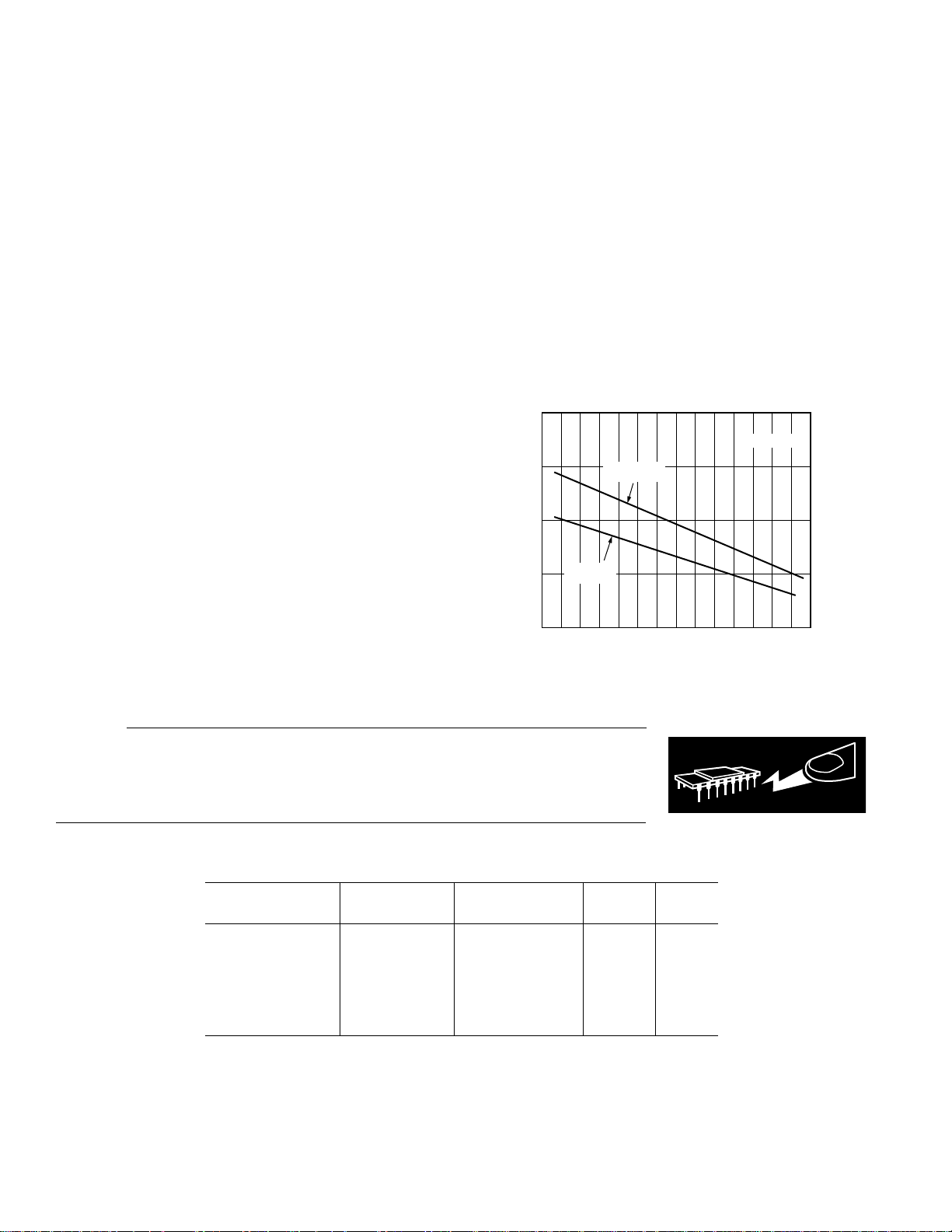
Figure 16. Distortion vs. Load Resistance; VS = ±5 V,
Frequency = 500 kHz
–40
3rd
R
= 100V
L
2nd
R
= 100V
3rd
RL = 1kV
L
G = +2
V
= 2V p-p
OUT
R
= 750V
F
10 20
–60
–80
DISTORTION 2 dBc
–100
2nd
RL = 1kV
1
FREQUENCY 2 MHz
Figure 19. Distortion vs. Load Resistance; VS = +5 V,
Frequency = 500 kHz
NORMALIZED GAIN 2 dB
Figure 17. Distortion vs. Frequency; VS = ±5 V
0.5
0.4
0.3
0.2
0.1
0
–0.1
–0.2
–0.3
–0.4
–0.5
0.1
Figure 18. Gain Flatness; VS = ±5 V
1
FREQUENCY 2 MHz
G = +2
VO = 0.3V p-p
R
= 750V
F
= 100V
R
L
= 65V
V
S
10 100
Figure 20. Distortion vs. Frequency; VS = +5 V
Figure 21. Gain Flatness; VS = +5 V
–7–REV. A
Page 8

AD8012
0
–10
–20
–30
–40
–60
–70
–80
100k 1M 10M 100M 500M
FREQUENCY – Hz
–50
–90
–100
PSRR – dB
VS = +5V OR 65V
G = +2
R
F
= 750V
–PSRR
+PSRR
NORMALIZED GAIN 2 dB
5
4
3
2
1
0
–1
–2
–3
–4
–5
1
G = +10
10
FREQUENCY 2 MHz
G = +2
100 500
VO = 0.3V p-p
R
= 750V
F
= 100V
R
L
= 65V
V
S
G = +1
Figure 22. Frequency Response; VS = ±5 V
–12
OUTPUT VOLTAGE 2 dBV
–15
–18
–21
9
6
3
1V RMS
0
–3
–6
–9
1
10
FREQUENCY 2 MHz
G = +2
RF = 750V
R
= 100V
L
= 65V
V
S
100 500
Figure 23. Output Voltage vs. Frequency; VS = ±5 V,
G = +2 V, R
= 100
L
Ω
5
4
3
2
1
0
–1
–2
NORMALIZED GAIN 2 dB
–3
–4
–5
1
G = +10
G = +2
10
FREQUENCY – MHz
VO = 0.3V p-p
R
= 750V
F
= 100V
R
L
V
= +5V
S
G = +1
100 500
Figure 25. Frequency Response; VS = +5 V
3
–12
–15
–18
OUTPUT VOLTAGE 2 dBV
–21
–24
–27
1VRMS
0
–3
–6
–9
1
10
FREQUENCY 2 MHz
G = +2
RF = 750V
R
= 100V
L
= +5V
V
S
100 500
Figure 26. Output Voltage vs. Frequency; VS = +5 V,
G = +2 V, R
= 100
L
Ω
0
–10
–20
–30
–40
–50
–60
CMRR 2 dB
–70
–80
–90
–100
Figure 24. CMRR vs. Frequency; VS = ±5 V, +5 V
VIN = 0.2V p-p
V
= 65V, +5V
S
10.03 0.1
FREQUENCY – MHz
10
100 500
Figure 27. PSRR vs. Frequency; VS = ±5 V, +5 V
–8– REV. A
Page 9

AD8012
1k
G = +2
RF = 750V
VS = +5V
10.03 0.1
FREQUENCY – MHz
10
VS = 65V
100 500
OUTPUT RESISTANCE 2 V
0.01
100
10
1
0.1
Figure 28. Output Resistance vs. Frequency
135
115
95
75
2 dB V
Z
55
T
35
15
–5
1E+03 1E+04 1E+05 1E+06 1E+07 1E+08 1E+09
FREQUENCY 2 Hz
TZ(s)
PHASE
0
–40
–80
–120
–160
–200
–240
–280
Figure 29. Open-Loop Transimpedance and Phase vs.
Frequency
PHASE – Degrees
4.0
3.8
3.6
Hz
3.4
3.2
3.0
INPUT VOLTAGE NOISE – nV/
2.8
2.6
2.4
2.2
2.0
100
FREQUENCY – Hz
CURRENT NOISE
+IN/–IN
VOLTAGE NOISE
10k1k
Figure 31. Noise vs. Frequency
9
8
f = 5MHz
G = 12
7
R
= 750V
F
6
5
4
3
2
1
0
PEAK-TO-PEAK OUTPUT AT 5MHz (#1% THD) 2 V
3 4 5 6 7 8 9 10 11
TOTAL SUPPLY VOLTAGE 2 Volts
RL = 1kV
RL = 100V
Figure 32. Output Swing vs. Supply
30
28
26
Hz
24
22
20
18
16
14
INPUT CURRENT NOISE – pA/
12
10
100k
9
8
7
6
5
4
SWING – V p-p
3
2
1
0
10
LOAD – V
Figure 30. Output Swing vs. Load
G = +2
R
65V
+5V
OUTPUT VOLTAGE ERROR – 0.1%/Div
0.1%
1k 10k100
= 750V
F
= 100V
R
L
2V STEP
5ns
t = 0
Figure 33. Settling Time, VS = ±5 V
–9–REV. A
Page 10

AD8012
5
VO = 0.3V p-p
R
F
R
L
G = +2
100 500
NORMALIZED GAIN 2 dB
4
3
2
1
0
–1
–2
–3
–4
–5
1
G = +10
10
FREQUENCY – MHz
Figure 34. Frequency Response; VS = ±5 V
0.5
0.4
0.3
0.2
0.1
0
–0.1
–0.2
NORMALIZED GAIN – dB
–0.3
–0.4
–0.5
0.1
FREQUENCY – MHz
VO = 0.3V p-p
G = +2
R
= 750V
F
= 1kV
R
L
101 100
Figure 35. Gain Flatness; VS = ±5 V
= 750V
= 1kV
G = +1
NORMALIZED GAIN 2 dB
5
4
3
2
1
0
–1
–2
–3
–4
–5
1
G = +10
10
FREQUENCY – MHz
VO = 0.3V p-p
R
F
R
L
G = +1
G = +2
100 500
Figure 37. Frequency Response; VS = +5 V
0.5
0.4
0.3
0.2
0.1
0
–0.1
–0.2
NORMALIZED GAIN – dB
–0.3
–0.4
–0.5
0.1
FREQUENCY – MHz
VO = 0.3V p-p
R
= 750V
F
= 1kV
R
L
101 100
Figure 38. Gain Flatness; VS = +5 V
= 750V
= 1kV
–20
DRIVER
–30
V
= 2V p-p
O
R
= 100V
L
SIDE 1
SIDE 2
10.03 0.1
FREQUENCY – MHz
INPUT REFERRED ERROR – dB
–40
–50
–60
–70
–80
–90
–100
–110
–120
Figure 36. Crosstalk vs. Frequency
+3V
V
OUT
V
0V
0V
–3V
V
, 2V/DIV
OUT
10
100 500
IN
V
IN
V
OUT
0V
0V
20ns
Figure 39. Overdrive Recovery; VS = ±5 V, G = +2,
R
= 750Ω, RL = 100Ω, VIN = 3 V p-p (T = 1µs)
F
–10– REV. A
Page 11

AD8012
THEORY OF OPERATION
The AD8012 is a dual high speed CF amplifier that attains new
levels of bandwidth (BW), power, distortion and signal swing
capability. Its wide dynamic performance (including noise) is
the result of both a new complementary high speed bipolar
process and a new and unique architectural design. The AD8012
basically uses a two gain stage complementary design approach
versus the traditional “single stage” complementary mirror
structure sometimes referred to as the Nelson amplifier. Though
twin stages have been tried before, they typically consumed
high power since they were of a folded cascade design much like
the AD9617. This design allows for the standing or quiescent
current to add to the high signal or slew current-induced stages.
In the time domain, the large signal output rise/fall time and
slew rate is typically controlled by the small signal BW of the
amplifier and the input signal step amplitude respectively, not
the dc quiescent current of the gain stages (with the exception
of input level shift diodes Q1/Q2). Using two stages vs. one
also allows for a higher overall gain bandwidth product (GBWP)
for the same power, thus lower signal distortion and the ability
to drive heavier external loads. In addition, the second gain
stage also isolates (divides down) A3’s input reflected load drive
and the nonlinearities created resulting in relatively lower distortion and higher open-loop gain.
Overall, when “high” external load drive and low ac distortion
is a requirement, a twin gain stage integrating amplifier like the
AD8012 will provide excellent results for lower power over the
traditional single stage complementary devices. In addition,
being a CF amplifier, closed-loop BW variations versus external gain variations (varying RN) will be much lower compared
to a VF op amp, where the BW varies inversely with gain. Another key attribute of this amplifier is its ability to run on a
single 5 V supply due in part to its wide common-mode input
and output voltage range capability. For 5 V supply operation,
the device obviously consumes half the quiescent power (vs.
10 V supply) with little degradation in its ac and dc performance characteristics. See data sheet comparisons.
DC GAIN CHARACTERISTICS
Gain stages A1/A1B and A2/A2B combined provide negative
feedforward transresistance gain. See Figure 40. Stage A3 is a
unity gain buffer which provides external load isolation to A2.
Each stage uses a symmetrical complementary design. (A3 is
also complementary though not explicitly shown). This is done
to reduce both second order signal distortion and overall quiescent power as discussed above. In the quasi dc to low frequency
region, the closed loop gain relationship can be approximated
as:
G = 1+R
G = –R
F/RN
F/RN
noninverting operation
inverting operation
These basic relationships above are common to all traditional
operational amplifiers.
A1
IPP
Q1
V
P
+–
Q2
INP
IPN
IQ1
Q3
V
N
Z
IE
Q4
IQ1
IPN
A1
C
CP2
A2
A2
D
ICQ + IO
VO 9
Z2
ICQ – IO
C
D
Z1 = R1 || C1
Z1
–V
I
CP1
IR + IFC
I
IR – IFC
–V
Z1
I
CP1
Figure 40. Simplified Block Diagram
A3
R
R
N
AD8012
V
R
F
L
O
C
L
–11–REV. A
Page 12

6V p-p
12V p-p
1:1
+5V
–5V
R
F
750V
R
F
750V
R
G
1.5kV
1/2
AD8012
1/2
AD8012
0.1mF
0.1mF
66.5V
66.5V
6V p-p
1:1
135V
TO
RECEIVER
CIRCUITRY
TO
RECEIVER
CIRCUITRY
GAIN = +2
UP TO
12,000 FEET
+
–
AD8012
APPLICATIONS
Line Driving for HDSL
High Bitrate Digital Subscriber Line (HDSL) is becoming
popular as a means of providing full duplex data communication
at rates up to 1.544 MBPS or 2.048 MBPS over moderate distances via conventional telephone twisted pair wires. Traditional
T1 (E1 in Europe) requires repeaters every 3,000 feet to 6,000
feet to boost the signal strength and allow transmission over
distances of up to 12,000 feet. In order to achieve repeaterless
transmission over this distance, an HDSL modem requires
transmitted power level of +13.5 dBm (assuming a line impedance of 135 Ω).
HDSL uses the Two Binary/One Quaternary line code (2B1Q).
A sample 2B1Q waveform is shown in Figure 41. The digital bit
stream is broken up into groups of two bits. Four analogue
voltages (called quaternary symbols) are used to represent the
four possible combinations of two bits. These symbols are assigned arbitrary names +3, +1, –1 and –3. The corresponding
voltage levels are produced by a DAC that is usually part of an
Analog Front End Circuit (AFEC). Before being applied to the
line, the DAC output is low-pass filtered and acquires the sinusoidal form shown in Figure 41. Finally, the filtered signal is
applied to the line driver. The line voltages that correspond to
the quaternary symbols +3, +1, –1 and –3 are 2.64 V, 0.88 V,
–0.88 V and –2.64 V. This gives a peak-to-peak line voltage of
5.28 V.
SYMBOL
VOLTAGE
NAME
+3 2.64V
+1 0.88V
–1 –0.88V
–3 –2.64V
–101+310+111–300–300+111+310–300–101–101+111–101–3
Figure 41. Time Domain Representation of a HDSL Signal
Many of the elements of a classic differential line driver are
shown in the HDSL line driver in Figure 42. A 6 V peak-topeak differential signal is applied to the input. The differential
gain of the amplifier (1+2 R
differential output signal is 12 V p-p.
As is normal in telephony applications, a transformer galvanically isolates the differential amplifier from the line. In this case
a 1:1 turns ratio is used. In order to correctly terminate the line,
it is necessary to set the output impedance of the amplifier to be
equal to the impedance of the line being driven (135 Ω in this
case). Because the transformer has a turns ratio of 1:1, the impedance reflected from the line is equal to the line impedance
of 135 Ω (R
resistors correctly terminate the line.
REFL
= R
LINE
DAC
OUTPUT
FILTERED
OUTPUT
TO LINE
DRIVER
) is set to +2, so the resulting
F/RG
/Turns Ratio
2
). As a result, two 66.5 Ω
00
Figure 42. Differential for HDSL Applications
The immediate effect of back-termination is that the signal from
the amplifier is halved before being applied to the line. This
doubles the power the amplifier must deliver. However, the
back-termination resistors also play an important second role.
Full-duplex data transmission systems like HDSL simultaneously transmit data in both directions. As a result, the signal
on the line and across the back termination resistors is the composite of the transmitted and received signal. The termination
resistors are used to tap off this signal and feed it to the receive
circuitry. Because the receive circuitry “knows” what is being
transmitted, the transmitted data can be subtracted from the
digitized composite signal to reveal the received data.
Driving a line with a differential signal offers a number of advantages compared to a single-ended drive. Because the two
outputs are always 180 degrees out of phase relative to one
another, the differential signal output is double the output amplitude of either of the op amps. As a result, the differential
amplifier can have a peak-to-peak swing of 16 V (each op amp
can swing to ±4 V), even though the power supply is ±5 V.
In addition to this, even-order harmonics (2nd, 4th, 6th, etc.) of
the two single-ended outputs tend to cancel out one another, so
the Total Harmonic Distortion (quadratic sum of all harmonics)
decreases compared to the single-ended case, even as the signal
amplitude is doubled. This is particularly advantageous for the
case of the second harmonic. As it is very close to the fundamental, filtering becomes difficult. In this application, the THD
is dominated by the third harmonic which is 65 dB below the
carrier (i.e., Spurious Free Dynamic Range = –65 dBc).
Differential line driving also helps to preserve the integrity of
the transmitted signal in the presence of Electro-Magnetic Interference (EMI). EMI tends to induce itself equally on to both
the positive and negative signal line. As a result, a receiver with
good common-mode rejection, will amplify the original signal
while rejecting induced (common-mode) EMI.
–12– REV. A
Page 13

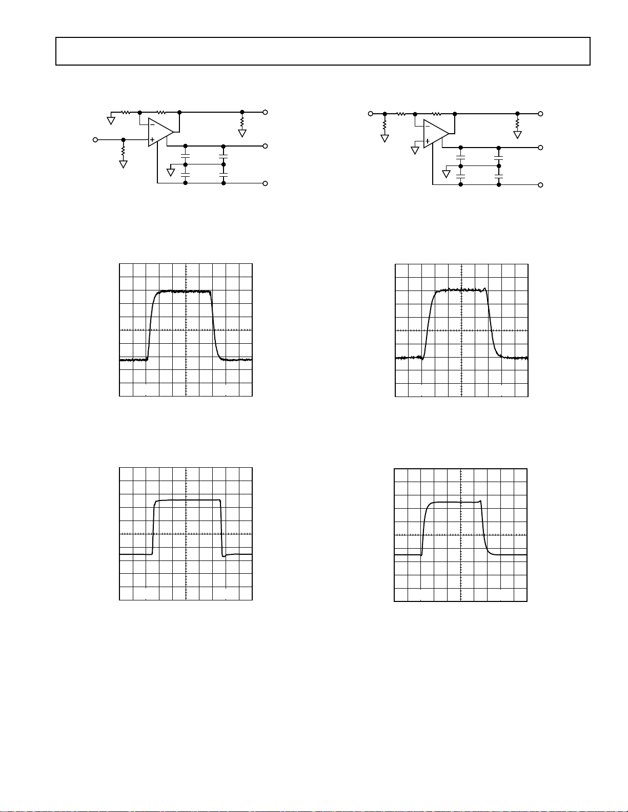
AD8012
0.1mF
INVERTING CONFIGURATION
V
OUT
R
F
RO*
10mF
NONINVERTING CONFIGURATION
V
OUT
R
G
R
F
RO*
R
T
0.1mF
10mF
R
T
V
IN
R
G
V
IN
*RO CHOSEN FOR CHARACTERISTIC IMPEDANCE.
*R
O
CHOSEN FOR CHARACTERISTIC IMPEDANCE.
+V
S
+
+
–V
S
Choosing the Appropriate Turns Ratio for the Transformer
Increasing the peak-to-peak output signal from the amplifier in
the previous example, combined with a variation in the turns
ratio of the transformer, can yield further enhancements to the
circuit. The output signal swing of the AD8012 can be increased
to about ±3.9 V before clipping occurs. This increases the peakto-peak output of the differential amplifier to 15.6 V. Because
the signal applied to the primary winding is now bigger, the
transformer turns ratio of 1:1 can be replaced with a (stepdown) turns ratio of about 1.3:1 (from amplifier to line). This
steps the 7.8 V peak-to-peak primary voltage down to 6 V. This
is the same secondary voltage as before so the resulting power
delivered to the line is the same.
The received signal, which is small relative to the transmitted
signal, will, however be stepped up by a factor of 1.3. Amplifying
the received signal in this manner enhances its signal-to-noise
ratio and is useful when the received signal is small compared to
the to-be-transmitted signal.
The impedance reflected from the 135 Ω line now becomes
228 Ω (1.3
2
times 135 Ω). With a correctly terminated line, the
amplifier must now drive a total load of 456 Ω (114 Ω + 114 Ω
+ 228 Ω), considerably less than the original 270 Ω load. This
reduces the drive current from the op amps by about 40%.
More significant however is the reduction in dynamic power
consumption; that is, the power the amplifier must consume in
order to deliver the load power. Increasing the output signal so
that it is as close as possible to the power rails, minimizes the
power consumed in the amplifier.
There is, however, a price to pay in terms of increased signal
distortion. Increasing the output signal of each op amp from the
original ±3 V to ±3.9 V reduces the Spurious Free Dynamic
Range (SFDR) from –65 dB to –50 dB (measured at 500 kHz),
even though the overall load impedance has increased from
270 Ω to 456 Ω.
The PCB should have a ground plane covering all unused portions of the component side of the board to provide a low impedance ground path. The ground plane should be removed
from the area near the input pins to reduce stray capacitance.
Chip capacitors should be used for supply bypassing (see Figure 43). One end should be connected to the ground plane
and the other within 1/8 in. of each power pin. An additional
(4.7 µF–10 µF) tantalum electrolytic capacitor should be con-
nected in parallel.
The feedback resistor should be located close to the inverting
input pin in order to keep the stray capacitance at this node to a
minimum. Capacitance greater than 1.5 pF at the inverting
input will significantly affect high speed performance when
operating at low noninverting gains.
Stripline design techniques should be used for long signal traces
(greater than about 1 in.). These should be designed with the
proper system characteristic impedance and be properly terminated at each end.
LAYOUT CONSIDERATIONS
The specified high speed performance of the AD8012 requires
careful attention to board layout and component selection.
Table I shows recommended component values for the AD8012
and Figures 44–49 show recommended layouts for the 8-lead
SOIC and microSOIC packages for a positive gain. Proper RF
design techniques and low parasitic component selections are
mandatory.
Figure 43. Inverting and Noninverting Configurations
Table I. Typical Bandwidth vs. Gain Setting Resistors
Small Signal –3 dB BW (MHz),
Gain R
F
R
G
R
T
VS = ⴞ5 V, RL = 1 k⍀
–1 750 Ω 750 Ω 53.6 Ω 110
+1 750 Ω – 49.9 Ω 350
+2 750 Ω 750 Ω 49.9 Ω 150
+10 750 Ω 82.5 Ω 49.9 Ω 40
RT chosen for 50 Ω characteristic input impedance.
–13–REV. A
Page 14

AD8012
Figure 44. Universal SOIC Noninverter Top Silkscreen
Figure 45. Universal SOIC Noninverter Top
Figure 47. Universal microSOIC Noninverter Top Silkscreen
Figure 48. Universal microSOIC Noninverter Top
Figure 46. Universal SOIC Noninverter Bottom
Figure 49. Universal microSOIC Noninverter Bottom
–14– REV. A
Page 15

0.1574 (4.00)
0.1497 (3.80)
0.0098 (0.25)
0.0040 (0.10)
OUTLINE DIMENSIONS
Dimensions shown in inches and (mm).
8-Lead SOIC
(SO-8)
0.1968 (5.00)
0.1890 (4.80)
8
5
0.2440 (6.20)
41
0.2284 (5.80)
PIN 1
0.0688 (1.75)
0.0532 (1.35)
0.0196 (0.50)
0.0099 (0.25)
AD8012
C3207a–0–12/99
x 45°
SEATING
PLANE
0.122 (3.10)
0.114 (2.90)
0.006 (0.15)
0.002 (0.05)
SEATING
PLANE
0.0500
(1.27)
BSC
0.122 (3.10)
0.114 (2.90)
8
1
PIN 1
0.0256 (0.65) BSC
0.120 (3.05)
0.112 (2.84)
0.018 (0.46)
0.008 (0.20)
0.0192 (0.49)
0.0138 (0.35)
0.0098 (0.25)
0.0075 (0.19)
8-Lead microSOIC
(RM-08)
5
0.199 (5.05)
0.187 (4.75)
4
0.043 (1.09)
0.037 (0.94)
0.011 (0.28)
0.003 (0.08)
8°
0°
0.0500 (1.27)
0.0160 (0.41)
0.120 (3.05)
0.112 (2.84)
33°
27°
0.028 (0.71)
0.016 (0.41)
PRINTED IN U.S.A.
–15–REV. A
 Loading...