

Datasheet AD8010AR-REEL7, AD8010AR-REEL, AD8010AR-16-REEL7, AD8010AR-16-REEL, AD8010AR-16 Datasheet (Analog Devices)
...Page 1
200 mA Output Current
16
15
14
13
1
2
3
4
NC = NO CONNECT
NC
–IN
+IN
NC
+V
S
OUT
NC
–V
S
12
11
10
9
5
6
7
8
NC
NC
NC
NC
NC
NC
NC
NC
AD8010
a
FEATURES
200 mA of Output Current
9 Load
SFDR –54 dBc @ 1 MHz
Differential Gain Error 0.04%, f = 4.43 MHz
Differential Phase Error 0.06, f = 4.43 MHz
Maintains Video Specifications Driving Eight Parallel
75 Loads
0.02% Differential Gain
0.03 Differential Phase
0.1 dB Gain Flatness to 60 MHz
THD –72 dBc @ 1 MHz, R
IP3 42 dBm @ 5 MHz, R
1 dB Gain Compression 21 dBm @ 5 MHz, R
230 MHz –3 dB Bandwidth, G = +1, R
800 V/s Slew Rate, R
25 ns Settling Time to 0.1%
Available in 8-Lead DIP, 16-Lead Wide Body SOIC and
Thermally Enhanced 8-Lead SOIC
APPLICATIONS
Video Distribution Amplifier
VDSL, xDSL Line Driver
Communications
ATE
Instrumentation
= 18.75
L
= 18.75
L
= 18.75
L
L
= 18.75
L
= 100
High-Speed Amplifier
AD8010
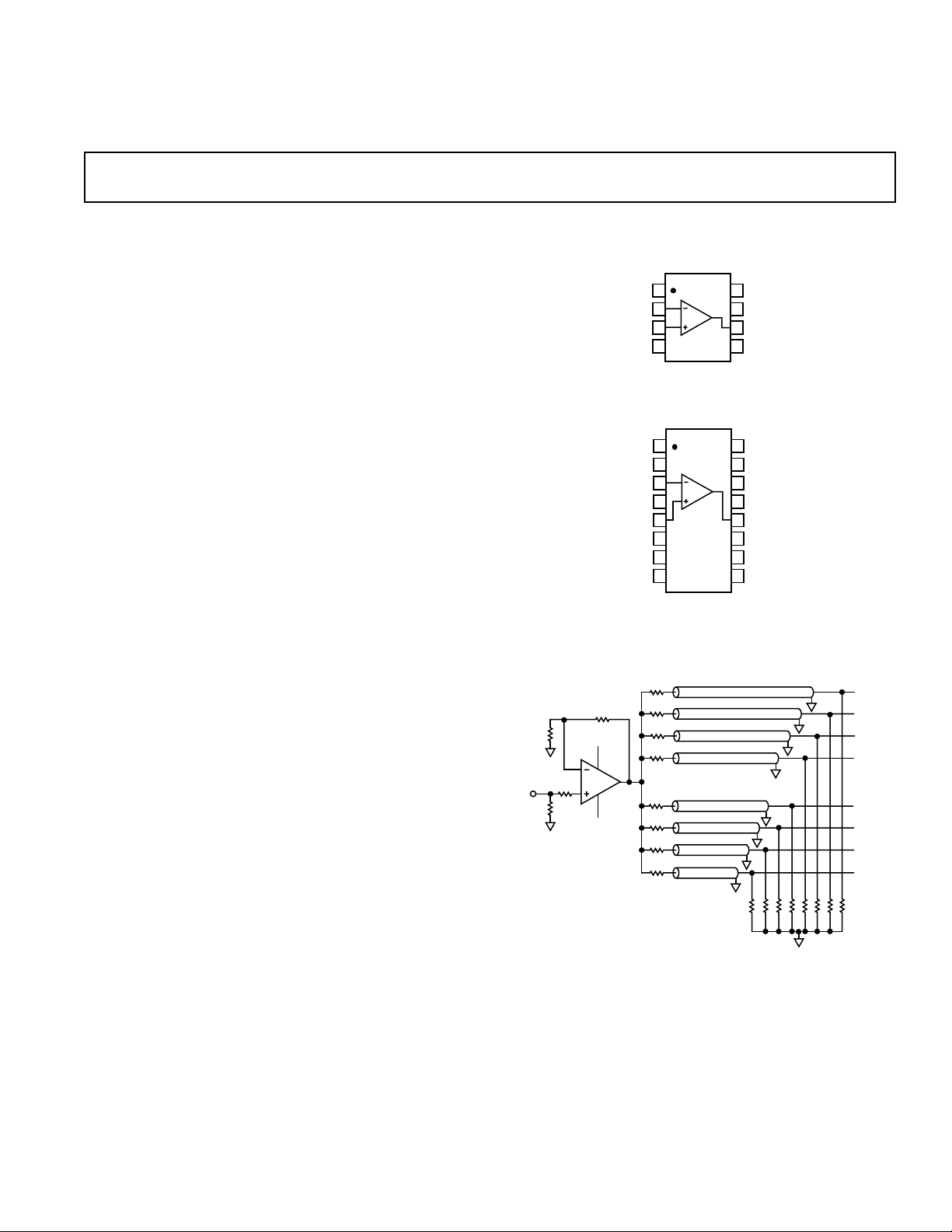
CONNECTION DIAGRAMS
8-Lead DIP and SOIC
AD8010
1
NC
2
–IN
3
+IN
4
S
NC = NO CONNECT
16-Lead Wide Body SOIC
8
NC
7
+V
S
6
OUT
5
NC–V
PRODUCT DESCRIPTION
The AD8010 is a low power, high current amplifier capable of
delivering a minimum load drive of 175 mA. Signal performance
such as 0.02% and 0.03° differential gain and phase error is
maintained while driving eight 75 Ω back terminated video lines.
The current feedback amplifier features gain flatness to 60 MHz
and –3 dB (G = +1) signal bandwidth of 230 MHz and only
requires a typical of 15.5 mA supply current from ±5 V supplies.
These features make the AD8010 an ideal component for Video
Distribution Amplifiers or as the drive amplifier within high data
rate Digital Subscriber Line (VDSL and xDSL) systems.
The AD8010 is an ideal component choice for any application
that needs a driver that will maintain signal quality when driving
low impedance loads.
The AD8010 is offered in three package options: an 8-lead DIP,
16-lead wide body SOIC and a low thermal resistance 8-lead
SOIC, and operates over the industrial temperature range of
–40°C to +85°C.
REV. B
Information furnished by Analog Devices is believed to be accurate and
reliable. However, no responsibility is assumed by Analog Devices for its
use, nor for any infringements of patents or other rights of third parties
which may result from its use. No license is granted by implication or
otherwise under any patent or patent rights of Analog Devices.
75
R
F
R
G
V
IN
R
T
+5V
AD8010
R
S
–5V
75
V
V
V
V
V
V
V
V
OUT1
OUT2
OUT3
OUT4
OUT5
OUT6
OUT7
OUT8
Figure 1. Video Distribution Amplifier
One Technology Way, P.O. Box 9106, Norwood, MA 02062-9106, U.S.A.
Tel: 781/329-4700 World Wide Web Site: http://www.analog.com
Fax: 781/326-8703 © Analog Devices, Inc., 2000
Page 2

AD8010–SPECIFICATIONS
RF = RG = 562 (N-8), RF = RG = 499 (R-8). T
M
odel Conditions Min Typ Max Unit
MIN
(@ 25C, VS = 5 V, G = +2, RL = 18.75 , RS+ = 150 , RF = RG = 604 (R-16),
= –40C, T
= +85C unless otherwise noted)
MAX
DYNAMIC PERFORMANCE
–3 dB Bandwidth G = +1, V
G = +2, V
0.1 dB Bandwidth V
Large Signal Bandwidth V
Peaking V
Slew V
Rise and Fall Time V
= 0.2 V p-p 30 60 MHz
OUT
= 4 V p-p 90 MHz
OUT
= 0.2 V p-p, < 5 MHz 0.02 dB
OUT
= 2 V p-p 800 V/µs
OUT
= 2 V p-p 2.0 ns
OUT
Settling Time 0.1%, V
= 0.2 V p-p 180 230 MHz
OUT
= 0.2 V p-p 130 190 MHz
OUT
= 2 V p-p 25 ns
OUT
NOISE/HARMONIC PERFORMANCE
Distortion V
= 2 V p-p
OUT
2nd Harmonic 1 MHz –73 dBc
5 MHz –58 dBc
10 MHz –53 dBc
10 MHz, R
= 39 Ω –67 dBc
L
20 MHz –44 dBc
3rd Harmonic 1 MHz –77 dBc
5 MHz –63 dBc
10 MHz –57 dBc
10 MHz, R
= 39 Ω –63 dBc
L
20 MHz –50 dBc
IMD 5 MHz ∆f = 10 kHz –73 dBc
IP3 5 MHz 42 dBm
1 dB Gain Compression 5 MHz 21 dBm
Input Noise Voltage f = 10 kHz 2 nV√Hz
Input Noise Current f = 10 kHz, +In 3 pA√Hz
f = 20 kHz, –In 20 pA√Hz
Differential Gain f = 4.43 MHz, R
= 150 Ω 0.02 %
L
f = 4.43 MHz, RL = 18.75 Ω 0.02 %
Differential Phase f = 4.43 MHz, R
= 150 Ω 0.02 Degrees
L
f = 4.43 MHz, RL =18.75 Ω 0.03 Degrees
DC PERFORMANCE
Input Offset Voltage 512mV
T
MIN–TMAX
15 mV
Offset Drift 10 µV/°C
Input Bias Current (–) 10 135 µA
T
MIN–TMAX
200 µA
Input Bias Current (+) 612µA
T
MIN–TMAX
20 µA
INPUT CHARACTERISTICS
Input Resistance +Input 125 kΩ
–Input 12.5 Ω
Input Capacitance 2.75 pF
Common-Mode Rejection Ratio V
= ±2.5 V 50 54 dB
CM
Input Common-Mode Voltage Range ±2.5 V
Open Loop Transresistance V
= ±2.5 V 300 500 kΩ
OUT
T
MIN–TMAX
250 kΩ
OUTPUT CHARACTERISTICS
Output Voltage Swing
RL = 18.75 Ω ±2.1 ±2.5 V
R
= 150 Ω ±2.7 ±3.0 V
L
Output Current RL = 9 Ω 175 200 mA
Short-Circuit Current 240 mA
Capacitive Load Drive 40 pF
POWER SUPPLY
Operating Range ±4.5 ±6.0 V
Quiescent Current 15.5 17 mA
T
MIN
to T
MAX
20 mA
Power Supply Rejection Ratio +VS = +4 V to +6 V, –VS = +5 V 60 66 dB
+VS = +5 V, –VS = –4 V to –6 V 50 56 dB
Specifications subject to change without notice.
–2–
REV. B
Page 3
AD8010
WARNING!
ESD SENSITIVE DEVICE
ABSOLUTE MAXIMUM RATINGS
Supply Voltage . . . . . . . . . . . . . . . . . . . . . . . . . . . . . . . 12.6 V
Internal Power Dissipation
2
1
Plastic Package (N) . . . . . . Observe Power Derating Curves
Small Outline Package (R) . Observe Power Derating Curves
Wide Body SOIC (R-16) . . . Observe Power Derating Curves
Input Voltage (Common-Mode) . . . . . . . . . . . . . . . . . . . ±V
S
Differential Input Voltage . . . . . . . . . . . . . . . . . . . . . . ± 1.2 V
Output Short Circuit Duration
. . . . . . . . . . . . . . . . . . . . . . Observe Power Derating Curves
Storage Temperature Range N, R . . . . . . . . –65°C to +125°C
Operating Temperature Range (A Grade) . . –40°C to +85°C
Lead Temperature Range (Soldering 10 sec) . . . . . . . . 300°C
NOTES
1
Stresses above those listed under Absolute Maximum Ratings may cause perma-
nent damage to the device. This is a stress rating only; functional operation of the
device at these or any other conditions above those indicated in the operational
section of this specification is not implied. Exposure to absolute maximum rating
conditions for extended periods may affect device reliability.
2
Specification is for device in free air:
8-Lead Plastic Package: θJA = 90°C/W
8-Lead SOIC Package: θJA = 122°C/W
16-Lead SOIC Package: θJA = 73°C/W
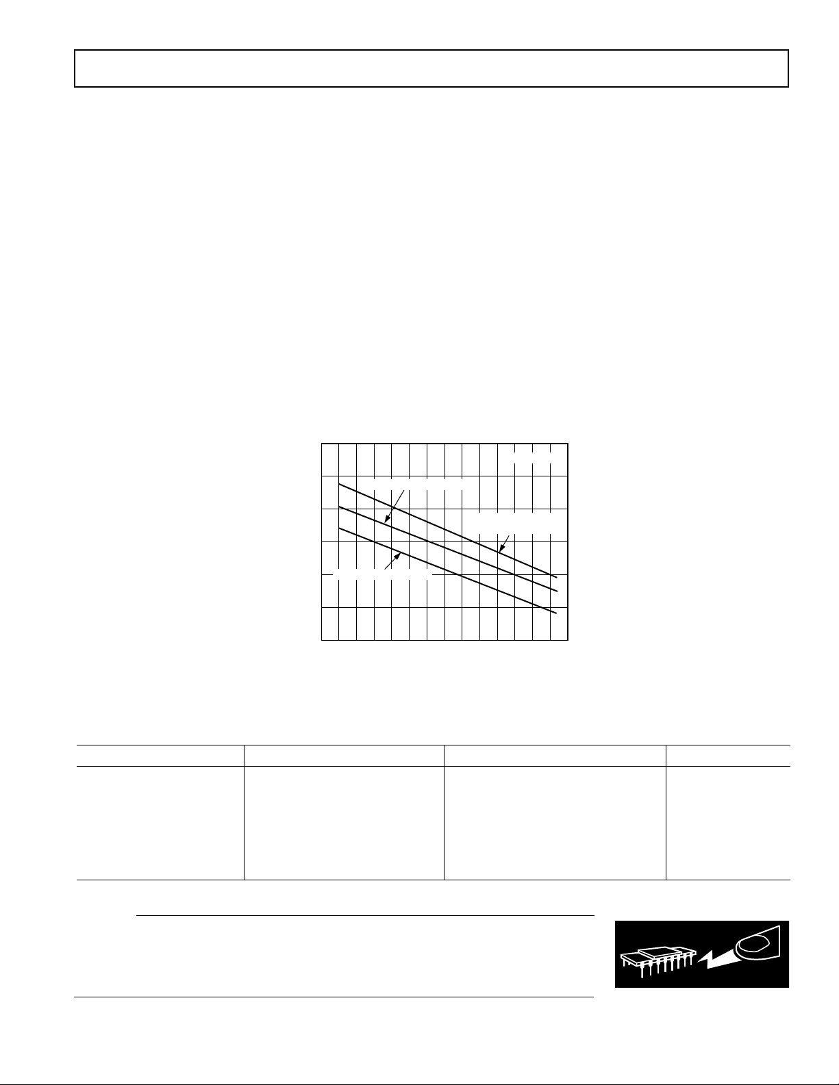
3.0
2.5
8-LEAD MINI-DIP PACKAGE
MAXIMUM POWER DISSIPATION
The maximum power that can be safely dissipated by the
AD8010 is limited by the associated rise in junction temperature.
The maximum safe junction temperature for plastic encapsulated devices is determined by the glass transition temperature
of the plastic, approximately +150°C. Temporarily exceeding
this limit may cause a shift in parametric performance due to a
change in the stresses exerted on the die by the package. Exceeding a junction temperature of +175°C for an extended period
can result in device failure.
While the AD8010 is internally short circuit protected, this
may not be sufficient to guarantee that the maximum junction
temperature (+150°C) is not exceeded under all conditions. To
ensure proper operation, it is necessary to observe the maximum
power derating curves.
TJ = 150C
2.0
1.5
1.0
8-LEAD SOIC PACKAGE
0.5
MAXIMUM POWER DISSIPATION – Watts
0
–40 –30 –20 –10 0 102030 40 5060708090
–50
AMBIENT TEMPERATURE – C
16-LEAD SOIC
PACKAGE (WIDEBODY)
Figure 2. Plot of Maximum Power Dissipation vs. Temperature
ORDERING GUIDE
Model Temperature Range Package Description Package Options
AD8010AN –40°C to +85°C 8-Lead Plastic DIP N-8
AD8010AR –40°C to +85°C 8-Lead Plastic SOIC SO-8
AD8010AR-16 –40°C to +85°C 16-Lead Wide Body SOIC R-16
AD8010AR-REEL REEL SOIC 13" REEL
AD8010AR-REEL7 REEL SOIC 7" REEL
AD8010AR-16-REEL REEL SOIC 13" REEL
AD8010AR-16-REEL7 REEL SOIC 7" REEL
CAUTION
ESD (electrostatic discharge) sensitive device. Electrostatic charges as high as 4000 V readily
accumulate on the human body and test equipment and can discharge without detection.
Although the AD8010 features proprietary ESD protection circuitry, permanent damage may
occur on devices subjected to high-energy electrostatic discharges. Therefore, proper ESD
precautions are recommended to avoid performance degradation or loss of functionality.
–3–REV. B
Page 4
AD8010
NUMBER OF VIDEO LOADS
0.05
0.04
DIFFERENTIAL PHASE
0
162 4 6 8 10 12 14
0.03
0.02
0.01
DIFFERENTIAL GAIN – %
1
0.10
0.08
0
0.06
0.04
0.02
DIFFERENTIAL PHASE – Degrees
DIFFERENTIAL GAIN
–Typical Performance Characteristics
60
50
40
30
20
PERCENTAGE OF UNITS
10
dG
d
dG
d
dG
0
0
dG
0.02 0.03 0.04 0.05 0.06 0.07 0.08 0.09 0.10 0.11 0.12
DIFFERENTIAL GAIN dG IN %
DIFFERENTIAL PHASE d IN Degrees
d
d
d
dG (%)/d – Degrees
SAMPLE SIZE = 300
G = +2
f = 4.43MHz (PAL)
= 18.75
R
L
d
d d d d d
0.130.01
Figure 3. Distribution of Differential Gain (dG) and
Differential Phase (d
–45
G = +2
–50
VO = 2V p-p
AS SHOWN
R
L
–55
–60
RL = 18.75
–65
–70
–75
–80
HARMONIC DISTORTION – dBc
–85
–90
–95
RL = 100
12 56789102034
φ
); RL = 18.75
2ND
3RD
3RD
2ND
FREQUENCY – MHz
Ω
Figure 4. Harmonic Distortion vs. Frequency; G = +2
Figure 6. Differential Gain and Phase vs. Number of Video
°
Loads Over Temperature (–40
45
40
35
30
25
20
INTERCEPT POINT – dBm
15
10
5
G = +2
= 18.75
R
L
1 10010
C to +85°C); f = 4.43 MHz
FREQUENCY – MHz
Figure 7. Two-Tone, 3rd Order IMD Intercept vs.
Frequency; G = +2, R
= 18.75
L
Ω
G = +2
6.20
R
= 18.75
L
= 0.2V p- p
V
O
6.15
6.10
6.05
6.0
5.95
5.90
GAIN FLATNESS – dB
5.85
5.80
0.1 1
FREQUENCY – MHz
Figure 5. Gain Flatness vs. Frequency Over Temperature
°
C to +85°C)
(–40
+85C
+25C
–40C
10 100
500
6.5
G = +2
6.4
= 0.2V p-p
V
O
NUMBER OF VIDEO
6.3
LOADS AS SHOWN
6.2
6.1
6.0
GAIN FLATNESS – dB
5.9
5.8
5.7
5.6
5.5
1
1
10
12
14
10 100
FREQUENCY – MHz
Figure 8. Gain Flatness vs. Frequency vs. Number of
Video Loads
–4–
4
2
6
8
1000
REV. B
Page 5

AD8010
FREQUENCY – MHz
010123456789
0
–10
–90
P
MEASURE
– dBm
–50
–60
–70
–80
–30
–40
–20
R
F
GAIN = 6.6
50
50
R
G
50
150
P
MEASURE
= 10dBm
(FULL SCALE)
500kHz TONE SPACING FROM
500kHz TO 5.5MHz WITH
4 MISSING TONES
FREQUENCY – MHz
8.0
0.0
1 100010
GAIN – dB
100
7.0
6.0
2.0
5.0
4.0
3.0
1.0
G = +2
V
O
= 0.2V p-p
NUMBER OF VIDEO LOADS AS SHOWN
12
4
1
8
–15
–25
–35
–45
–55
–65
–75
INTERMODULATION DISTORTION – dBm
–85
5
–5
P
4dBm
OUT
G = +2
= 18.75
R
L
= 5MHz
f
O
= 10kHz
f
–69dBm –69dBm
FREQUENCY – MHz
4dBm
Figure 9. Intermodulation Distortion
–35
FREQUENCY = 5MHz
G = +2
–45
= AS SHOWN (SEE SCHEMATIC)
R
L
–55
RL = 18.75
–65
–75
–85
–95
TOTAL HARMONIC DISTORTION – dBc
–105
–10 12–8
RL = 100
P
R
= FOR RL = 100
L1
= 23.1 FOR RL = 18.75
R
L1
–6 –4 –20 246810
IN
P
– dBm
OUT
R
R
G
150
50
Figure 10. Total Harmonic Distortion vs. P
5.0355.0155.04.9854.965
Figure 12. Multitone Distortion; RL = 100
–55
G = +2
–60
–65
–70
–75
F
50
P
L1
OUT
OUT
50
; G = +2
R
–80
HARMONIC DISTORTION – dBc
–85
–90
15 100 200 300 400 500
Figure 13. Harmonic Distortion vs. Load
ND
2
RD
3
LOAD –
VO = 2V p-p
f = 5MHz
Ω
2
1
0
–1
–2
–3
GAIN AS SHOWN
–4
Figure 11. Small Signal Closed-Loop Frequency
Response; R
VO = 0.2V p-p
NORMALIZED GAIN – dB
= 18.75
R
L
–5
–6
–7
0.1 10001
= 18.75
L
FREQUENCY – MHz
Ω
G = +1
G = +2
G = +3
10 100
Figure 14. Closed-Loop Frequency Response vs.
Number of Video Loads
–5–REV. B
Page 6

AD8010
g
–10
–20
–30
–40
–50
PSRR – dB
–60
–70
–80
0.03
–PSRR
+PSRR
0.1
1 10 100
FREQUENCY – MHz
500
Figure 15. PSRR vs. Frequency
310
G = +2
100
31
10
3.1
1
0.31
0.1
0.031
CLOSED-LOOP OUTPUT RESISTANCE –
0.1
1
FREQUENCY – MHz
10 100
500
Figure 16. Closed-Loop Output Resistance vs. Frequency
0
–10
–20
–30
–40
–50
–60
CMRR – dB
–70
–80
–90
–100
0.1 5001
10 100
FREQUENCY – MHz
Figure 18. CMRR vs. Frequency
1000
316
100
31.6
10
3.16
TRANSRESISTANCE – k
1
0.316
10k 1G100k
PHASE
TRANSRESISTANCE
1M 10M 100M
FREQUENCY – Hz
0
45
90
135
180
225
Figure 19. Transresistance and Phase vs. Frequency;
= 18.75
R
L
Ω
rees
PHASE – De
2
1
0
–1
GAIN AS SHOWN
= 2V p-p
V
O
–2
= 18.75
R
L
–3
–4
NORMALIZED GAIN – dB
–5
–6
–7
0.1 10001
G = +2
G = +10
10 100
FREQUENCY – MHz
G = +1
Figure 17. Large Signal Frequency Response; VO = 2 V p-p
3.0
2.0
G = +2
100
NORMALIZED GAIN – dB
1.0
0.0
–1.0
–2.0
–3.0
–4.0
–5.0
–6.0
–7.0
GAIN AS SHOWN
= 4V p-p
V
O
= 18.75
R
L
0.1
0
FREQUENCY – MHz
G = +10
10
Figure 20. Large Signal Frequency Response; VO = 4 V p-p
–6–
1000
REV. B
Page 7

0.2
INVERTING CURRENT
NONINVERTING CURRENT
100
10
1
10 100 1k 10k 100k 1M
FREQUENCY – Hz
INPUT CURRENT NOISE – pA/ Hz
1000
10M
0.15
0.1
0.05
VOLTS
–0.05
–0.1
–0.15
–0.2
0
50mV 20ns
G = +1
R
= 18.75
L
V
= 0.2V p-p
O
5
4
3
2
1
0
VOLTS
–1
–2
–3
–4
–5
AD8010
G = +1
R
= 18.75
L
V
= 4V p-p
O
1V
20ns
Figure 21. Small-Signal Pulse Response; G = +1
0.2
0.15
0.1
0.05
VOLTS
–0.05
–0.1
–0.15
–0.2
0
50mV
G = +2, –1
R
= 18.75
L
V
= 0.2V p-p
O
20ns
Figure 22. Small-Signal Pulse Response; G = +2, –1
100
Figure 24. Large-Signal Pulse Response; G = +1
4
3
2
1
0
VOLTS
–1
–2
–3
–4
1V
G = +2, –1
R
= 18.75
L
V
= 4V p-p
O
20ns
Figure 25. Large-Signal Pulse Response; G = +2, –1
10
INPUT VOLTAGE NOISE – nV/ Hz
1
10 100
Figure 23. Input Voltage Noise vs. Frequency
10k
1k
FREQUENCY – Hz
100k
1M
10M
Figure 26. Input Current Noise vs. Frequency
–7–REV. B
Page 8

AD8010
G = +6
R
= 604
F
R
= 18.75
L
INPUT
OUTPUT
0
VOLTS
INPUT (500mV/DIV)
OUTPUT (1V/DIV)
100ns
Figure 27. Overdrive Recovery; G = +6
OVERDRIVE RECOVERY
Overdrive of an amplifier occurs when the output and/or input
range are exceeded. The amplifier must recover from this overdrive condition. As shown in Figure 27, the AD8010 recovers
within 35 ns from negative overdrive and within 75 ns from
positive overdrive.
THEORY OF OPERATION
The AD8010 is a current feedback amplifier optimized for high
current output while maintaining excellent performance with
respect to flatness, distortion and differential gain/phase. As a
video distribution amplifier, the AD8010 will drive up to 12
parallel video loads (12.5 Ω) from a single output with 0.04%
differential gain and 0.04° differential phase errors. This means
that, unlike designs with one driver per output, any output is a
true reflection of the signal on all other outputs.
The high output current capability of the AD8010 also make it
useful in xDSL applications. The AD8010 can drive a 12.5 Ω
single-ended or 25 Ω differential load with low harmonic distortion. This makes it useful in designs that utilize a step-up
transformer to drive a twisted-pair transmission line.
To achieve these levels of performance special precautions with
respect to supply bypassing are recommended (Figure 29). This
configuration minimizes the contribution from high frequency
supply rejection to differential gain and phase errors as well as
reducing distortion due to harmonic energy in the power supplies.
200
100
G = +5
10
CAPACITIVE LOAD – pF
G = +2
1
0205
R
R
V
IN
F
G
150
50
RS –
GAIN AS SHOWN
= 0.2V p-p
V
O
w/ 30% OVERSHOOT
R
S
V
OUT
C
L
G = +1
10 15
Figure 28. Capacitive Load Drive vs. Series Resistor for
Various Gains
Driving Capacitance Loads
The AD8010 was designed primarily to drive nonreactive loads.
If driving loads with a capacitive component is desired, best
frequency response is obtained by the addition of a small series
resistance as shown in Figure 28. The inset figure shows the
optimum value for R
vs. capacitive load. It is worth noting
SERIES
that the frequency response of the circuit when driving large
capacitive loads will be dominated by the passive roll-off of
and CL.
R
SERIES
LAYOUT CONSIDERATIONS
The specified high speed performance of the AD8010 requires
careful attention to board layout and component selection.
Proper R
design techniques and low-pass parasitic component
F
selection are necessary.
The PCB should have a ground plane covering all unused portions
of the component side of the board to provide low impedance
path. The ground plane should be removed from the area near
the input pins to reduce the parasitic capacitance.
–V
+V
V
150
IN
R
T
AD8010
S
S
FB
C1
+
R
BT
C2
+
R
F
R
G
Z
O
R
L
Figure 29. Standard Noninverting Closed-Loop Configuration with Recommended Bypassing Technique
The standard noninverting closed-loop configuration with the
recommended power supply bypassing technique is shown in
Figure 29. Ferrite beads (Amidon Associates, Torrance CA,
Part Number 43101) are used to suppress high frequency power
supply energy on the DUT supply lines at the DUT. C1 and C2
each represent the parallel combination of a 47 µF (16 V) tanta-
lum electrolytic capacitor, a 10 µF (10 V) tantalum electrolytic
capacitor and a 0.1 µF ceramic chip capacitor. Connect C1
from the +V
pin to the –VS pin. Connect C2 from the –VS pin
S
to signal ground.
The feedback resistor should be located close to the inverting
input pin in order to keep the parasitic capacitance at this node
to a minimum. Parasitic capacitances of less than 1 pF at the
inverting input can significantly affect high speed performance.
Stripline design techniques should be used for long traces
(greater than about 3 cm). These should be designed with a
characteristic impedance (Z
) of 50 Ω or 75 Ω and be properly
O
terminated at each end.
–8–
REV. B
Page 9

AD8010
APPLICATIONS
Video Distribution Amplifier
The AD8010 is optimized for the specific function of providing
excellent video performance when driving multiple video loads
in parallel. Significant power is saved and heat sinking is greatly
simplified because of the ability of the AD8010 to obtain this
performance when running on a ±5 V supply. However, due to
the high currents that flow when driving many parallel video
loads, special layout and bypassing techniques are required to
assure optimal performance.
When designing a video distribution amplifier with the AD8010, it
is very important to keep in mind where the high (ac) currents
will flow. These paths include the power supply pins of the chip
along with the bypass capacitors and the return path for these
capacitors, the output circuits and the return path of the output
current from the loads.
In general, any loops that are formed by any of the above paths
should be made as small as possible. Large loops are both generators and receivers of magnetic fields and can cause undesired
coupling of signals that lowers the performance of the amplifier.
Effects that have not been seen before in other op amp circuits
might arise because of the high currents. Most op amp circuits
output, at most, tens of milliamps and do not require extremely
tight video specifications, while a video distribution amplifier
can output hundreds of milliamps and require extremely low
differential gain and phase errors.
The bypassing scheme that is used for the AD8010 requires
special attention. It was found that the conventional technique
of bypassing each power pin individually to ground can have an
adverse effect on the differential phase error of the circuit. The
cause of this is attributed to the fact that there is an internal
compensation capacitor in the AD8010 that is referenced to the
negative supply.
The recommended technique is to connect parallel bypass
capacitors from the positive supply to the negative supply and
then to bypass the negative supply to ground. For high frequency bypassing, 0.1 µF ceramic capacitors are recommended.
These should be placed within a few millimeters of the power
pins and should preferably be chip type capacitors.
The high currents that can potentially flow through the power
supply pins require large bypassing capacitors. These should be
low inductance tantalum types and at least 47 µF. The ground
side of the capacitor that bypasses the negative supply should be
brought to a single point ground that is the common for the
returns of the outputs.
Figure 30 shows a circuit for making an N-channel video distribution amplifier. As a practical matter, the AD8010 can readily
drive eight standard 150 Ω video loads. When driving up to 12
video loads, there is minimal degradation in video performance.
Another important consideration when driving multiple cables
is the high frequency isolation between the outputs of the
cables. Due to its low output impedance, the AD8010 achieves
better than 46 dB of output-to-output isolation at 5 MHz driving back terminated 75 Ω cables.
+5V
FB
499499
V
IN
150
75
AD8010
C1
C2
FB
–5V
75
75
75
75
75 R
75 R
R
L1
L2
LN
Figure 30. An N-Channel Video Distribution Amplifier Using An AD8010.
NOTE: Please see Figure 29 for Recommended Bypassing Technique.
–9–REV. B
Page 10

AD8010
Differential Line Driver
Twisted pair transmission lines are more often being used for
high frequency analog and digital signals. Over long distances,
however, the attenuation characteristics of these lines can
degrade the performance of the transmission system. To compensate for this, larger signals are transmitted, which after the
attenuation, will still have useful signal strength.
The high output current of two AD8010s can be used along
with a transformer to create a high power differential line driver.
The differential configuration effectively doubles the output
swing, while the step-up transformer further increases the output voltage.
499
499
AD8010
150
V
IN
402
806
12.4
In the circuit in Figure 31 the A device is configured as a gainof-two follower, while the B device is a gain-of-two inverter.
These will produce a differential output signal whose maximum
value is twice the peak-to-peak value of the maximum output
of one device. For this circuit a 12 V peak-to-peak output can
be obtained.
The op amps drive a 1:2 step-up transformer that drives a
100 Ω transmission line. Since the impedance reflected back to
the primary varies as the square of the turns ratio, it will appear
as 25 Ω at the primary. This source terminating resistor is split
as a 12.4 Ω resistor at the output of each device.
The circuit shown is capable of delivering 12 V p-p to the line
and operates with a –3 dB bandwidth of 40 MHz. The peak
current output of either op amp is 100 mA.
+6
100
AD8010
150
12.4
1:2
–6
Figure 31. High Output Differential Line Driver Using Two AD8010s.
NOTE: Please see Figure 29 for Recommended Bypassing Technique.
–10–
REV. B
Page 11

AD8010
Closed-Loop Gain and Bandwidth
The AD8010 is a current feedback amplifier optimized for use
in high performance video and data acquisition applications.
Since it uses a current feedback architecture, its closed-loop
–3 dB bandwidth is dependent on the magnitude of the feedback
resistor. The desired closed-loop bandwidth and gain are obtained
by varying the feedback resistor (R
varying the gain resistor (R
G
) to set the bandwidth, and
F
) to set the desired gain. The characteristic curves and specifications for this data sheet reflect the
performance of the AD8010 using the values of R
noted at the
F
top of the specifications table. If a greater –3 dB bandwidth
and/or slew rate is required (at the expense of video performance),
Table I provides the recommended resistor values. Figure 32
shows the test circuit and conditions used to produce Table I.
Effect of Feedback Resistor Tolerance on Gain Flatness
Because of the relationship between the 3 dB bandwidth and the
feedback resistor, the fine scale gain flatness will, to some extent,
vary with feedback resistor tolerance. It is therefore recommended
that resistors with a 1% tolerance be used if it is desired to maintain flatness over a wide range of production lots. In addition,
resistors of different construction have different associated parasitic capacitance and inductance. Metal-film resistors were used
for the bulk of the characterization for this data sheet. It is possible that values other than those indicated will be optimal for
other resistor types.
Quality of Coaxial Cable
Optimum flatness when driving a coax cable is possible only
when the driven cable is terminated at each end with a resistor
matching its characteristic impedance. If the coax was ideal,
then the resulting flatness would not be affected by the length of
the cable. While outstanding results can be achieved using inexpensive cables, it should be noted that some variation in flatness
due to varying cable lengths may be experienced.
Table I. –3 dB Bandwidth and Slew Rate vs. Closed-Loop
Gain and Resistor Values
Package: N-8
Closed-Loop –3 dB BW Slew Rate
Gain RF ()RG () (MHz) (V/s)
+1 453
∞
285 900
+2 374 374 255 900
+5 348 86.6 200 800
+10 562 61.9 120 550
Package: R-16
Closed-Loop –3 dB BW Slew Rate
Gain RF ()RG () (MHz) (V/s)
+1 412
∞
245 900
+2 392 392 220 900
+5 392 97.6 160 800
+10 604 66.5 95 550
Package: SO-8
Closed-Loop –3 dB BW Slew Rate
Gain RF ()RG () (MHz) (V/s)
+1 392
∞
345 950
+2 374 374 305 1000
+5 348 86.6 220 1000
+10 499 54.9 135 650
1. VO = 0.2 V p-p for –3 dB Bandwidth.
2. VO = 2 V p-p for Slew Rate.
3. Bypassing per Figure 29.
50
150
V
R
F
18.75
OUT
V
IN
R
G
Figure 32. Test Circuit for Table I
–11–REV. B
Page 12

AD8010
0.210 (5.33)
MAX
0.160 (4.06)
0.115 (2.93)
0.022 (0.558)
0.014 (0.356)
0.1574 (4.00)
0.1497 (3.80)
OUTLINE DIMENSIONS
Dimensions shown in inches and (mm).
8-Lead Plastic Mini-DIP
(N-8)
0.430 (10.92)
0.348 (8.84)
8
14
PIN 1
0.100
(2.54)
BSC
5
0.280 (7.11)
0.240 (6.10)
0.060 (1.52)
0.015 (0.38)
0.070 (1.77)
0.045 (1.15)
0.130
(3.30)
MIN
SEATING
PLANE
0.325 (8.25)
0.300 (7.62)
0.015 (0.381)
0.008 (0.204)
8-Lead SOIC
(SO-8)
0.1968 (5.00)
0.1890 (4.80)
8
5
0.2440 (6.20)
41
0.2284 (5.80)
0.195 (4.95)
0.115 (2.93)
C01047a–0–12/00 (rev. B)
0.0098 (0.25)
0.0040 (0.10)
SEATING
0.0118 (0.30)
0.0040 (0.10)
PIN 1
0.0500
(1.27)
PLANE
BSC
16-Lead Wide Body SOIC
0.4133 (10.50)
0.3977 (10.00)
16 9
PIN 1
0.0192 (0.49)
0.0500
(1.27)
0.0138 (0.35)
BSC
0.0688 (1.75)
0.0532 (1.35)
0.0192 (0.49)
0.0138 (0.35)
81
0.1043 (2.65)
0.0926 (2.35)
0.0098 (0.25)
0.0075 (0.19)
(R-16)
0.2992 (7.60)
0.2914 (7.40)
SEATING
PLANE
8
0
0.4193 (10.65)
0.3937 (10.00)
0.0125 (0.32)
0.0091 (0.23)
0.0196 (0.50)
0.0099 (0.25)
0.0500 (1.27)
0.0160 (0.41)
0.0291 (0.74)
0.0098 (0.25)
0.0500 (1.27)
8
0
0.0157 (0.40)
45
45
PRINTED IN U.S.A.
–12–
REV. B
 Loading...