

Page 1
Ultralow Distortion
FREQUENCY – MHz
–30
–40
–110
1 10010
DISTORTION – dBc
–70
–80
–90
–100
–50
–60
THIRD
G = +2
R
L
= 150⍀
V
S
= 5V
V
OUT
= 2V p-p
SECOND
High Speed Amplifiers
AD8007/AD8008
FEATURES
Extremely Low Distortion
Second Harmonic
–88 dBc @ 5 MHz
–83 dBc @ 20 MHz (AD8007)
–77 dBc @ 20 MHz (AD8008)
Third Harmonic
–101 dBc @ 5 MHz
–92 dBc @ 20 MHz (AD8007)
–98 dBc @ 20 MHz (AD8008)
High Speed
650 MHz, –3 dB Bandwidth (G = +1)
1000 V/s Slew Rate
Low Noise
2.7 nV/
22.5 pA/
Hz Input Voltage Noise
√
Hz Input Inverting Current Noise
√
Low Power
9 mA/Amplifier Typ Supply Current
Wide Supply Voltage Range
5 V to 12 V
0.5 mV Typical Input Offset Voltage
Small Packaging
SOIC-8, MSOP, and SC70 Packages Available
APPLICATIONS
Instrumentation
IF and Baseband Amplifiers
Filters
A/D Drivers
DAC Buffers
GENERAL DESCRIPTION
The AD8007 (single) and AD8008 (dual) are high performance current feedback amplifiers with ultralow distortion
and noise. Unlike other high performance amplifiers, the low
price and low quiescent current allow these amplifiers to be
used in a wide range of applications. ADI’s proprietary second
generation eXtra-Fast Complementary Bipolar (XFCB)
process enables such high performance amplifiers with low
power consumption.
The AD8007/AD8008 have 650 MHz bandwidth, 2.7 nV/√Hz
voltage noise, –83 dB SFDR @ 20 MHz (AD8007), and –77 dBc
SFDR @ 20 MHz (AD8008).
With the wide supply voltage range (5 V to 12 V) and wide bandwidth, the AD8007/AD8008 are designed to work in a variety of
applications. The AD8007/AD8008 amplifiers have a low power
supply current of 9 mA/amplifier.
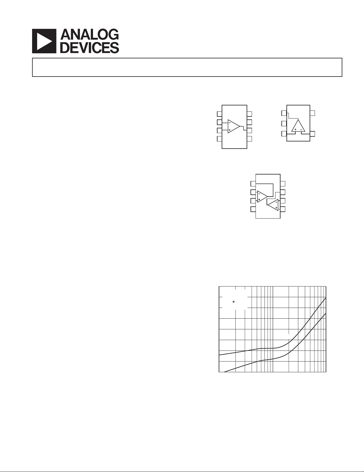
CONNECTION DIAGRAMS
SOIC (R) SC70 (KS-5)
AD8007
1
NC
(Top View)
2
–IN
3
+IN
–V
4
S
NC = NO CONNECT
8
NC
7
+V
6
V
5
NC
V
S
OUT
OUT
–V
+IN
S
AD8007
1
(Top View)
2
3
5
+V
S
4
–IN
SOIC (R) and MSOP (RM)
AD8008
(Top View)
1
V
OUT1
–IN1
27
36
+IN1
–V
45
S
8
+V
S
V
OUT2
–IN2
+IN2
The AD8007 is available in a tiny SC70 package as well as a
standard 8-lead SOIC. The dual AD8008 is available in both
8-lead SOIC and 8-lead MSOP packages. These amplifiers are
rated to work over the industrial temperature range of –40°C
to +85°C.
Figure 1. AD8007 Second and Third Harmonic
Distortion vs. Frequency
REV. D
Information furnished by Analog Devices is believed to be accurate and
reliable. However, no responsibility is assumed by Analog Devices for its
use, nor for any infringements of patents or other rights of third parties that
may result from its use. No license is granted by implication or otherwise
under any patent or patent rights of Analog Devices. Trademarks and
registered trademarks are the property of their respective companies.
One Technology Way, P.O. Box 9106, Norwood, MA 02062-9106, U.S.A.
Tel: 781/329-4700 www.analog.com
Fax: 781/326-8703 © 2003 Analog Devices, Inc. All rights reserved.
Page 2

AD8007/AD8008–SPECIFICATIONS
VS = ⴞ5 V
Parameter Conditions Min Typ Max Unit
DYNAMIC PERFORMANCE
–3 dB Bandwidth G = +1, VO = 0.2 V p-p, RL = 1 kΩ 540 650 MHz
Bandwidth for 0.1 dB Flatness VO = 0.2 V p-p, G = +2, RL = 150 Ω 50 90 MHz
Overdrive Recovery Time ±2.5 V Input Step, G = +2, R
Slew Rate G = +1, V
Settling Time to 0.1% G = +2, VO = 2 V Step 18 ns
Settling Time to 0.01% G = +2, VO = 2 V Step 35 ns
NOISE/HARMONIC PERFORMANCE
Second Harmonic fC = 5 MHz, VO = 2 V p-p –88 dBc
Third Harmonic f
IMD f
Third Order Intercept f
Crosstalk (AD8008) f = 5 MHz, G = +2 –68 dB
Input Voltage Noise f = 100 kHz 2.7 nV/√Hz
Input Current Noise –Input, f = 100 kHz 22.5 pA/√Hz
Differential Gain Error NTSC, G = +2, R
Differential Phase Error NTSC, G = +2, RL = 150 Ω 0.010 Degree
DC PERFORMANCE
Input Offset Voltage 0.5 4 mV
Input Offset Voltage Drift 3 µV/°C
Input Bias Current +Input 4 8 µA
Input Bias Current Drift +Input 16 nA/°C
Transimpedance V
INPUT CHARACTERISTICS
Input Resistance +Input 4 MΩ
Input Capacitance +Input 1 pF
Input Common-Mode Voltage Range –3.9 to +3.9 V
Common-Mode Rejection Ratio VCM = ±2.5 V 56 59 dB
OUTPUT CHARACTERISTICS
Output Saturation Voltage VCC – VOH, VOL – VEE, RL = 1 kΩ 1.1 1.2 V
Short Circuit Current, Source 130 mA
Short Circuit Current, Sink 90 mA
Capacitive Load Drive 30% Overshoot 8 pF
POWER SUPPLY
Operating Range 5 12 V
Quiescent Current per Amplifier 9 10.2 mA
Power Supply Rejection Ratio
+PSRR 59 64 dB
–PSRR 59 65 dB
(@ TA = 25ⴗC, RS = 200 ⍀, RL = 150 ⍀, RF = 499 ⍀, Gain = +2, unless otherwise noted.)
AD8007/AD8008
G = +1, V
G = +2, V
G = +1, V
= 20 MHz, VO = 2 V p-p –83/–77 dBc
f
C
= 5 MHz, VO = 2 V p-p –101 dBc
C
= 20 MHz, VO = 2 V p-p –92/–98 dBc
f
C
= 19.5 MHz to 20.5 MHz, RL = 1 kΩ,
C
V
= 5 MHz, RL = 1 kΩ 43.0/42.5 dBm
C
= 20 MHz, RL = 1 kΩ 42.5 dBm
f
C
= 0.2 V p-p, RL = 150 Ω 250 500 MHz
O
= 0.2 V p-p, RL = 150 Ω 180 230 MHz
O
= 2 V p-p, RL = 1 kΩ 200 235 MHz
O
= 1 kΩ 30 ns
= 2 V Step 900 1000 V/µs
O
= 2 V p-p –77 dBc
O
L
+Input, f = 100 kHz 2 pA/√Hz
= 150 Ω 0.015 %
L
–Input 0.4 6 µA
–Input 9 nA/°C
= ±2.5 V, RL = 1 kΩ 1.0 1.5 MΩ
O
RL = 150 Ω 0.4 0.8 MΩ
REV. D–2–
Page 3

AD8007/AD8008
VS = 5 V
(@ TA = 25ⴗC, RS = 200 ⍀, RL = 150 ⍀, RF = 499 ⍀, Gain = +2, unless otherwise noted.)
AD8007/AD8008
Parameter Conditions Min Typ Max Unit
DYNAMIC PERFORMANCE
–3 dB Bandwidth G = +1, V
= 0.2 V p-p, RL = 1 kΩ 520 580 MHz
O
G = +1, VO = 0.2 V p-p, RL = 150 Ω 350 490 MHz
G = +2, V
G = +1, V
= 0.2 V p-p, RL = 150 Ω 190 260 MHz
O
= 1 V p-p, RL = 1 kΩ 270 320 MHz
O
Bandwidth for 0.1 dB Flatness Vo = 0.2 V p-p, G = +2, RL = 150 Ω 72 120 MHz
Overdrive Recovery Time 2.5 V Input Step, G = +2, R
Slew Rate G = +1, V
= 2 V Step 665 740 V/µs
O
= 1 kΩ 30 ns
L
Settling Time to 0.1% G = +2, VO = 2 V Step 18 ns
Settling Time to 0.01% G = +2, VO = 2 V Step 35 ns
NOISE/HARMONIC PERFORMANCE
Second Harmonic f
Third Harmonic f
IMD f
Third Order Intercept f
= 5 MHz, VO = 1 V p-p –96/–95 dBc
C
f
= 20 MHz, VO = 1 V p-p –83/–80 dBc
C
= 5 MHz, VO = 1 V p-p –100 dBc
C
= 20 MHz, VO = 1 V p-p –85/–88 dBc
f
C
= 19.5 MHz to 20.5 MHz, RL = 1 kΩ, –89/–87 dBc
C
= 1 V p-p
V
O
= 5 MHz, RL = 1 kΩ 43.0 dBm
C
f
= 20 MHz, RL = 1 kΩ 42.5/41.5 dBm
C
Crosstalk (AD8008) Output to Output f = 5 MHz, G = +2 –68 dB
Input Voltage Noise f = 100 kHz 2.7 nV/√Hz
Input Current Noise –Input, f = 100 kHz 22.5 pA/√Hz
+Input, f = 100 kHz 2 pA/√Hz
DC PERFORMANCE
Input Offset Voltage 0.5 4 mV
Input Offset Voltage Drift 3 µV/°C
Input Bias Current +Input 4 8 µA
–Input 0.7 6 µA
Input Bias Current Drift +Input 15 nA/°C
–Input 8 nA/°C
Transimpedance V
= 1.5 V to 3.5 V, RL = 1 kΩ 0.5 1.3 MΩ
O
RL = 150 Ω 0.4 0.6 MΩ
INPUT CHARACTERISTICS
Input Resistance +Input 4 MΩ
Input Capacitance +Input 1 pF
Input Common-Mode Voltage Range 1.1 to 3.9 V
Common-Mode Rejection Ratio VCM = 1.75 V to 3.25 V 54 56 dB
OUTPUT CHARACTERISTICS
Output Saturation Voltage VCC – VOH, VOL – VEE, RL = 1 kΩ 1.05 1.15 V
Short Circuit Current, Source 70 mA
Short Circuit Current, Sink 50 mA
Capacitive Load Drive 30% Overshoot 8 pF
POWER SUPPLY
Operating Range 5 12 V
Quiescent Current per Amplifier 8.1 9 mA
Power Supply Rejection Ratio
+PSRR 59 62 dB
–PSRR 59 63 dB
REV. D
–3–
Page 4
AD8007/AD8008
ABSOLUTE MAXIMUM RATINGS*
Supply Voltage . . . . . . . . . . . . . . . . . . . . . . . . . . . . . . . . 12.6 V
Power Dissipation . . . . . . . . . . . . . . . . . . . . . . . . See Figure 2
Common-Mode Input Voltage . . . . . . . . . . . . . . . . . . . . . ±V
S
Differential Input Voltage . . . . . . . . . . . . . . . . . . . . . . ± 1.0 V
Output Short Circuit Duration . . . . . . . . . . . . . . See Figure 2
Storage Temperature . . . . . . . . . . . . . . . . . . –65°C to +125°C
Operating Temperature Range . . . . . . . . . . . –40°C to +85°C
Lead Temperature Range (soldering 10 sec) . . . . . . . . . 300°C
*Stresses above those listed under Absolute Maximum Ratings may cause perma-
nent damage to the device. This is a stress rating only; functional operation of the
device at these or any other conditions above those indicated in the operational
section of this specification is not implied. Exposure to absolute maximum rating
conditions for extended periods may affect device reliability.
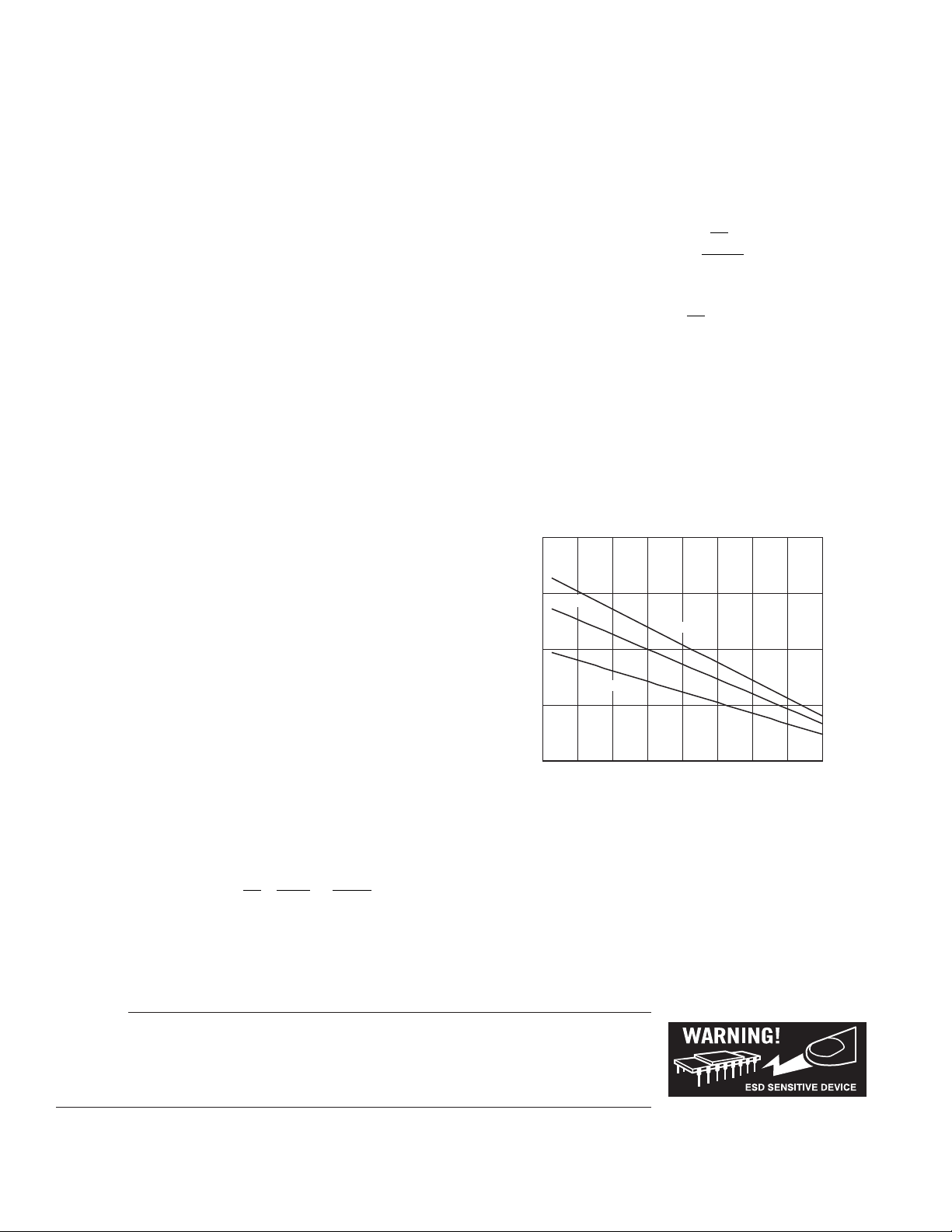
MAXIMUM POWER DISSIPATION
The maximum safe power dissipation in the AD8007/AD8008
packages is limited by the associated rise in junction temperature
) on the die. The plastic encapsulating the die will locally reach
(T
J
the junction temperature. At approximately 150°C, which is the
glass transition temperature, the plastic will change its properties. Even temporarily exceeding this temperature limit may
change the stresses that the package exerts on the die, permanently shifting the parametric performance of the AD8007/
AD8008. Exceeding a junction temperature of 175°C for an
extended period of time can result in changes in the silicon
devices, potentially causing failure.
The still-air thermal properties of the package and PCB (θ
ambient temperature (T
package (P
) determine the junction temperature of the die.
D
), and the total power dissipated in the
A
),
JA
The junction temperature can be calculated as follows:
TT P
=+ ×
ADA
JJ
θ
()
The power dissipated in the package (PD) is the sum of the quiescent power dissipation and the power dissipated in the package
due to the load drive for all outputs. The quiescent power is the
voltage between the supply pins (V
). Assuming the load (RL) is referenced to midsupply, the
(I
S
total drive power is V
/2 ⫻ I
S
package and some in the load (V
) times the quiescent current
S
, some of which is dissipated in the
OUT
OUT
⫻ I
). The difference
OUT
between the total drive power and the load power is the drive
power dissipated in the package.
P
= quiescent power + (total drive power – load power):
D
PVI
=×
()
DSS
+×
VVRV
S OUT
2
L
2
OUT
−
R
L
RMS output voltages should be considered. If RL is referenced
, as in single-supply operation, then the total drive power
to V
S
⫻ I
is V
S
OUT
.
If the rms signal levels are indeterminate, then consider the
worst case, when V
= VS/4 for RL to midsupply:
OUT
V
S
4
PVI
=×
()
DSS
+
R
L
2
In single-supply operation, with RL referenced to VS, worst case is
V
V
OUT
S
=
2
Airflow will increase heat dissipation, effectively reducing θJA.
Also, more metal directly in contact with the package leads from
metal traces, through holes, ground, and power planes will
reduce the θ
. Care must be taken to minimize parasitic capaci-
JA
tances at the input leads of high speed op amps as discussed in
the board layout section.
Figure 2 shows the maximum safe power dissipation in the package versus ambient temperature for the SOIC-8 (125°C/W),
MSOP (150°C/W), and SC70 (210°C/W) packages on a JEDEC
standard 4-layer board. θ
2.0
1.5
MSOP-8
1.0
0.5
MAXIMUM POWER DISSIPATION – W
0
–60 100–40
values are approximations.
JA
SOIC-8
SC70-5
–20 0 20 406080
AMBIENT TEMPERATURE – ⴗC
Figure 2. Maximum Power Dissipation vs.
Temperature for a 4-Layer Board
OUTPUT SHORT CIRCUIT
Shorting the output to ground or drawing excessive current for
the AD8007/AD8008 will likely cause catastrophic failure.
CAUTION
ESD (electrostatic discharge) sensitive device. Electrostatic charges as high as 4000 V readily
accumulate on the human body and test equipment and can discharge without detection. Although the
AD8007/AD8008 features proprietary ESD protection circuitry, permanent damage may occur on
devices subjected to high energy electrostatic discharges. Therefore, proper ESD precautions are
recommended to avoid performance degradation or loss of functionality.
REV. D–4–
Page 5

AD8007/AD8008
ORDERING GUIDE
Package
Model Temperature Range Description Package Outline Branding
AD8007AR –40°C to +85°C 8-Lead SOIC R-8
AD8007AR-REEL –40°C to +85°C 8-Lead SOIC R-8
AD8007AR-REEL7 –40°C to +85°C 8-Lead SOIC R-8
AD8007AKS-R2 –40°C to +85°C 5-Lead SC70 KS-5 HTA
AD8007AKS-REEL –40°C to +85°C 5-Lead SC70 KS-5 HTA
AD8007AKS-REEL7 –40°C to +85°C 5-Lead SC70 KS-5 HTA
AD8008AR –40°C to +85°C 8-Lead SOIC R-8
AD8008AR-REEL7 –40°C to +85°C 8-Lead SOIC R-8
AD8008AR-REEL –40°C to +85°C 8-Lead SOIC R-8
AD8008ARM –40°C to +85°C 8-Lead MSOP RM-8 H2B
AD8008ARM-REEL –40°C to +85°C 8-Lead MSOP RM-8 H2B
AD8008ARM-REEL7 –40°C to +85°C 8-Lead MSOP RM-8 H2B
REV. D
–5–
Page 6
AD8007/AD8008–Typical Performance Characteristics
(VS = ⴞ5 V, RL = 150 ⍀, RS = 200 ⍀, RF = 499 ⍀, unless otherwise noted.)
3
2
1
0
–1
–2
–3
–4
NORMALIZED GAIN – dB
–5
–6
–7
1 10010
G = +10
G = –1
FREQUENCY – MHz
G = +1
G = +2
1000
TPC 1. Small Signal Frequency Response for Various Gains
3
G = +1
2
1
0
–1
–2
GAIN – dB
–3
–4
–5
–6
–7
RL = 150⍀, VS = ⴞ5V
RL = 150⍀, VS = +5V
10010
FREQUENCY – MHz
RL = 1k⍀, VS = ⴞ5V
1000
6.4
G = +2
6.3
6.2
6.1
6.0
5.9
GAIN – dB
5.8
5.7
5.6
5.5
5.4
FREQUENCY – MHz
VS = +5V
VS = ⴞ5V
10010
TPC 4. 0.1 dB Gain Flatness; VS = +5, ±5 V
9
G = +2
8
7
6
5
4
GAIN – dB
3
2
1
0
–1
RL = 150⍀, VS = ⴞ5V
RL = 1k⍀, VS = ⴞ5V
FREQUENCY – MHz
10010
RL = 1k⍀, VS = +5V
RL = 150⍀
= +5V
V
S
1000
1000
TPC 2. Small Signal Frequency Response for VS and R
3
G = +1
2
= 1k⍀
R
L
1
0
–1
–2
GAIN – dB
–3
–4
–5
–6
–7
RS = 301⍀
10010
FREQUENCY – MHz
RS = 200⍀
RS = 249⍀
1000
TPC 3. Small Signal Frequency Response for
Various R
Values
S
LOAD
TPC 5. Small Signal Frequency Response for VS and R
9
G = +2
8
7
6
5
4
GAIN – dB
3
2
1
0
–1
RF = RG = 499⍀
RF = RG = 649⍀
10010
FREQUENCY – MHz
RF = RG = 324⍀
RF = RG = 249⍀
1000
TPC 6. Small Signal Frequency Response for Various
Feedback Resistors, R
F=RG
LOAD
REV. D–6–
Page 7

10
FREQUENCY – Hz
10M
1M
10k 1M100k
TRANSIMPEDANCE – ⍀
1k
100
10
1
100k
10k
10M
100M 1G
0
–30
–90
–150
–210
–270
–330
PHASE – Degrees
2G
TRANSIMPEDANCE
PHASE
30
90
–180
FREQUENCY – MHz
9
8
1
10010
GAIN – dB
5
4
3
2
7
6
0
–1
1000
G = +2
VS = +5V, +85ⴗC
VS = ⴞ5V, –40ⴗC
VS = +5V, –40ⴗC
VS = ⴞ5V, +85ⴗC
FREQUENCY – MHz
9
8
1
10010
GAIN – dB
5
4
3
2
7
6
0
–1
1000
RL = 150⍀, VS = ⴞ5V, VO = 2V p-p
RL = 1k⍀, VS = ⴞ5V, VO = 2V p-p
RL = 150⍀, VS = +5V, VO = 1V p-p
RL = 1k⍀, VS = +5V, VO = 1V p-p
G = +2
G = +2
9
8
7
6
5
GAIN – dB
4
3
2
1
0
499⍀
200⍀
49.9⍀
1 10010
499⍀
R
SNUB
C
LOAD
FREQUENCY – MHz
20pF AND
20⍀ SNUB
20pF
0pF
20pF AND
10⍀ SNUB
AD8007/AD8008
1000
TPC 7. Small Signal Frequency Response for Capacitive
Load and Snub Resistor
TPC 9. Large Signal Frequency Response for Various Gains
REV. D
3
2
1
0
–1
–2
GAIN – dB
–3
–4
–5
–6
–7
G = +1
VS = +5V, –40ⴗC
VS = ⴞ5V, –40ⴗC
10010
FREQUENCY – MHz
VS = +5V, +85ⴗC
VS = ⴞ5V, +85ⴗC
TPC 8. Small Signal Frequency Response over
Temperature, VS = +5 V, ±5 V
3
V
= 2V p-p
OUT
2
G = +2
G = +1
1
0
–1
–2
–3
–4
NORMALIZED GAIN – dB
–5
–6
–7
1 10010
G = +10
G = –1
FREQUENCY – MHz
1000
1000
TPC 10. Transimpedance and Phase vs. Frequency
TPC 11. Small Signal Frequency Response over
Temperature, V
= +5 V, ±5 V
S
TPC 12. Large Signal Frequency Response for VS and R
–7–
LOAD
Page 8

AD8007/AD8008
–40
–50
–60
–70
–80
DISTORTION – dBc
–90
–100
–110
G = ⴙ1
= 5V
V
S
= 1V p-p
V
O
HD2, RL = 1k⍀
HD3, RL = 1k⍀
FREQUENCY – MHz
HD3, RL = 150⍀
101
HD2, RL = 150⍀
100
TPC 13. AD8007 Second and Third Harmonic Distortion
vs. Frequency and R
–40
G = ⴙ1
= ⴞ5V
V
S
–50
= 2V p-p
V
O
–60
–70
HD2, RL = 1k⍀
–80
DISTORTION – dBc
–90
–100
L
HD3, RL = 150⍀
HD2, R
HD3, RL = 1k⍀
= 150⍀
L
–40
G = ⴙ2
V
= 5V
S
–50
= 1V p-p
V
O
–60
–70
–80
DISTORTION – dBc
–90
–100
–110
HD3, RL = 1k⍀
FREQUENCY – MHz
HD2, RL = 1k⍀
HD2, RL = 150⍀
HD3, RL = 150⍀
101
100
TPC 16. AD8007 Second and Third Harmonic Distortion
vs. Frequency and R
–40
G = ⴙ2
= ⴞ5V
V
S
–50
= 2V p-p
V
O
–60
–70
–80
DISTORTION – dBc
–90
–100
L
HD2, RL = 1k⍀
HD2, RL = 150⍀
HD3, RL = 150⍀
HD3, RL = 1k⍀
–110
101
FREQUENCY – MHz
100
TPC 14. AD8007 Second and Third Harmonic Distortion
vs. Frequency and R
–30
VS = ⴞ5V
= 2V p-p
V
O
–40
= 150⍀
R
L
–50
–60
–70
–80
DISTORTION – dBc
–90
–100
–110
L
HD3, G = ⴙ10
FREQUENCY – MHz
HD2, G = ⴙ10
HD2, G = ⴙ1
101
HD3, G = ⴙ1
100
TPC 15. AD8007 Second and Third Harmonic Distortion
vs. Frequency and Gain
–110
101
FREQUENCY – MHz
100
TPC 17. AD8007 Second and Third Harmonic Distortion
vs. Frequency and R
–30
G = +2
V
= 5V
S
–40
= 150⍀
R
L
–50
–60
–70
–80
DISTORTION – dBc
–90
–100
–110
L
HD2, VO = 4V p-p
HD2, VO = 2V p-p
FREQUENCY – MHz
HD3, VO = 4V p-p
HD3, VO = 2V p-p
101
100
TPC 18. AD8007 Second and Third Harmonic Distortion
vs. Frequency and V
OUT
REV. D–8–
Page 9

FREQUENCY – MHz
10010
HD2, RL = 1k⍀
HD2, RL = 150⍀
HD3, RL = 1k⍀
HD3, R
L
= 150⍀
G = 2
V
S
= 5V
V
O
= 1V p-p
–40
1
DISTORTION – dBc
–110
–100
–90
–80
–70
–60
–50
(VS = ⴞ5 V, RS = 200 ⍀, RF = 499 ⍀, RL = 150 ⍀, @ 25°C, unless otherwise noted.)
–40
G = 1
V
= 5V
S
–50
= 1V p-p
V
O
–60
–70
–80
DISTORTION – dBc
–90
–100
–110
HD2, RL = 1k⍀
1
TPC 19. AD8008 Second and Third Harmonic
Distortion vs. Frequency and R
–40
G = 1
= 5V
V
S
–50
= 1V p-p
V
O
–60
HD2, RL = 150⍀
HD3, RL = 150⍀
FREQUENCY – MHz
HD3, RL = 1k⍀
L
10010
TPC 22. AD8008 Second and Third Harmonic
Distortion vs. Frequency and R
–40
–50
–60
G = 2
VS = 5V
= 2V p-p
V
O
AD8007/AD8008
L
HD2, R
= 1k⍀
L
DISTORTION – dBc
–100
–110
TPC 20. AD8008 Second and Third Harmonic
Distortion vs. Frequency and R
DISTORTION – dBc
–100
–110
TPC 21. AD8008 Second and Third Harmonic
Distortion vs. Frequency and Gain
REV. D
–70
HD2, RL = 150⍀
–80
HD2, RL = 1k⍀
–90
HD3, RL = 1k⍀
1 10010
–30
VS = 5V
= 2V p-p
V
–40
O
= 150 ⍀
R
L
–50
–60
–70
–80
HD2, G = 1
–90
HD3, G = 10
1
HD3, RL = 150⍀
FREQUENCY – MHz
HD2, G = 10
HD3, G = 1
FREQUENCY – MHz
–70
1
HD2, RL = 150⍀
HD3, R
= 1k⍀
L
FREQUENCY – MHz
HD3, RL = 150⍀
10010
–80
DISTORTION – dBc
–90
–100
–110
TPC 23. AD8008 Second and Third Harmonic
L
10010
Distortion vs. Frequency and R
–30
G = 2
= 150⍀
R
L
–40
= 5V
V
S
–50
–60
HD2, VO = 4V p-p
–70
–80
DISTORTION – dBc
–90
–100
–110
1
HD2, VO = 2V p-p
HD3, VO = 4V p-p
FREQUENCY – MHz
L
HD3, V
= 2V p-p
O
10010
TPC 24. AD8008 Second and Third Harmonic
Distortion vs. Frequency and V
OUT
–9–
Page 10

AD8007/AD8008
–60
G = ⴙ2
V
F
–65
–70
–75
–80
DISTORTION – dBc
–85
–90
= 5V
S
= 20MHz
O
1.51
HD2, R
V
OUT
= 1k⍀
L
– V p-p
HD3, R
L
HD3, RL = 150⍀
HD2, R
L
2
= 1k⍀
= 150⍀
TPC 25. AD8007 Second and Third Harmonic
Distortion vs. V
44
43
42
41
40
39
38
37
THIRD ORDER INTERCEPT – dBm
36
35
5
10 15 20 25 30 35 40 45 50 55 60 65 70
and R
OUT
FREQUENCY – MHz
L
G = +2
= ⴞ5V
V
S
= 2V p-p
V
O
= 1k⍀
R
L
2.5
–65
–70
–75
–80
–85
–90
–95
DISTORTION – dBc
–100
–105
–110
G = ⴙ2
= ⴞ5V
V
S
= 20MHz
F
O
HD2, RL = 150⍀
21
HD3, RL = 1k⍀
HD3, RL = 150⍀
34
V
OUT
HD2, RL = 1k⍀
56
– V p-p
TPC 28. AD8007 Second and Third Harmonic
Distortion vs. V
44
43
42
41
40
39
38
37
THIRD ORDER INTERCEPT – dBm
36
35
and R
OUT
FREQUENCY – MHz
L
G = ⴙ2
= 5V
V
S
= 2V p-p
V
O
= 1k⍀
R
L
6560555045403530252015105
70
TPC 26. AD8007 Third Order Intercept vs. Frequency
–65
G = ⴙ2
= 5V
V
S
= 20MHz
–70
–75
–80
–85
–90
F
O
HD2, R
= 1k⍀
L
1.51
HD2, R
HD3, R
HD3, R
V
OUT
= 150⍀
L
L
= 1k⍀
L
– V p-p
= 150⍀
2
2.5
TPC 27. AD8008 Second and Third Harmonic
Distortion vs. V
OUT
and R
L
TPC 29. AD8008 Third Order Intercept vs. Frequency
–65
–70
–75
–80
–85
–90
–95
–100
–105
–110
HD2, RL = 150⍀
HD3, RL = 1k⍀
1
HD2, RL = 1k⍀
HD3, RL = 150⍀
G = ⴙ2
= 5V
V
S
= 20MHz
F
O
26
345
V
– V p-p
OUT
TPC 30. AD8008 Second and Third Harmonic
Distortion vs. V
OUT
and R
L
REV. D–10–
Page 11

FREQUENCY – Hz
10 10k100
CURRENT NOISE – pA/ Hz
100
10
1
100k
1M
1000
10M1k
NONINVERTING CURRENT NOISE 2.0pA/ Hz
INVERTING CURRENT NOISE 22.5pA / Hz
FREQUENCY – Hz
100k 1G
CROSSTALK – dB
–100
1M
10M 100M
–90
–80
–70
–60
–50
–40
–20
–30
G = ⴙ2
R = 150⍀
V
S
= ⴞ5V
V
M
= 1V p-p
SIDE B DRIVEN
SIDE A DRIVEN
FREQUENCY – Hz
20
10
10k 1M100k
PSRR – dB
–20
–30
–40
–50
0
–10
10M
100M 1G
–60
–70
–80
+PSRR
–PSRR
(VS = ⴞ5 V, RL = 150 ⍀, RS = 200 ⍀, RF = 499 ⍀, unless otherwise noted.)
100
10
2.7nV/ Hz
VOLTA G E NOISE – nV/ Hz
AD8007/AD8008
1
10 1k100
FREQUENCY – Hz
10k
100k 1M
TPC 31. Input Voltage Noise vs. Frequency
1000
G = ⴙ2
100
10
1
OUTPUT IMPEDANCE – ⍀
0.1
0.01
100k 10M1M
FREQUENCY – Hz
100M
TPC 32. Output Impedance vs. Frequency
0
VS = ⴞ5V, ⴙ5V
–10
–20
TPC 34. Input Current Noise vs. Frequency
1G
TPC 35. AD8008 Crosstalk vs. Frequency (Output to Output)
–30
–40
CMRR – dB
–50
–60
REV. D
–70
100k
1M
FREQUENCY – Hz
TPC 33. CMRR vs. Frequency
10M
100M 1G
TPC 36. PSRR vs. Frequency
–11–
Page 12

AD8007/AD8008
R
G = ⴙ1
= 150⍀, VS = ⴙ5V AND ⴞ5V
L
R
= 1k⍀, VS = ⴙ5V AND ⴞ5V
L
50mV/DIV
010
20 30 40 50
TIME – ns
TPC 37. Small Signal Transient Response for
RL= 150Ω, 1 kΩ and VS = +5 V, ±5 V
G = +1
1V/DIV
R
L
R
= 150⍀
= 1k⍀
L
G = +2
01020304050
R
= 150⍀, VS = +5V AND 5V
L
RL = 1k⍀, VS = +5V AND 5V
50mV/DIV
TIME – ns
TPC 40. Small Signal Transient Response for
= 150 Ω, 1 kΩ and VS = +5 V, ±5 V
R
L
G = –1
INPUT
OUTPUT
1V/DIV
01020304050
TIME – ns
TPC 38. Large Signal Transient Response for
RL= 150 Ω, 1 k
G = ⴙ2
010 20 304050
1V/DIV
Ω
C
= 0pF
LOAD
C
= 10pF
LOAD
C
= 20pF
LOAD
TIME – ns
TPC 39. Large Signal Transient Response
for Capacitive Load = 0 pF, 10 pF, and 20 pF
010203040 50
TIME – ns
TPC 41. Large Signal Transient Response, G = –1,
= 150
R
L
Ω
499⍀
200⍀
49.9⍀
50mV/DIV
CL = 0pF
CL = 20pF
499⍀
–
+
C
LOAD
TIME – ns
CL = 20pF
= 10⍀
R
SNUB
R
SNUB
G = ⴙ2
010 20304050
TPC 42. Small Signal Transient Response: Effect of
Series Snub Resistor when Driving Capacitive Load
REV. D–12–
Page 13

G = ⴙ2
ⴙV
S
ⴚV
S
0 100 200
RL = 150⍀
OUTPUT (2V/DIV)
INPUT (1V/DIV)
TIME – ns
RL = 1k⍀
300 400 500
– V
V
OUT
–1
–2
–3
–4
AD8007/AD8008
4
G = +10
V
3
2
1
0
2000
400 600
RL – ⍀
= 5V
S
= 0.75V
V
IN
800 1000
TPC 43. Output Overdrive Recovery, RL = 1 kΩ,
150 Ω, VIN = ±2.5 V
0.5
0.4
0.3
0.2
0.1
0
ⴚ0.1
ⴚ0.2
SETTLING TIME – %
ⴚ0.3
ⴚ0.4
ⴚ0.5
0
18ns
51015202530354045
TIME – ns
G = +2
TPC 44. 0.1% Settling Time, 2 V Step
TPC 45. V
OUT
VIN=±0.75 V
Swing vs. R
, VS=±5 V, G = +10,
LOAD
REV. D
–13–
Page 14

AD8007/AD8008
THEORY OF OPERATION
The AD8007 (single) and AD8008 (dual) are current feedback
amplifiers optimized for low distortion performance. A simplified
conceptual diagram of the AD8007 is shown in Figure 3. It closely
resembles a classic current feedback amplifier comprised of a
complementary emitter-follower input stage, a pair of signal mirrors, and a diamond output stage. However, in the case of the
AD8007/AD8008, several modifications have been made to greatly
improve the distortion performance over that of a classic current
feedback topology.
+V
Q5
Q6
OUT
S
–V
S
IN+
M1
I
–
I
–
1
CJ1
+V
D1
D2
I
–
2
Q1
IN–
I
DI
Q2
S
HiZ
–V
S
CJ2
M2
R
G
3
Q3
I
DO
Q4
–
I
4
R
F
Figure 3. Simplified Schematic of AD8007
The signal mirrors have been replaced with low distortion, high
precision mirrors. They are shown as “M1” and “M2” in Figure 3.
Their primary function from a distortion standpoint is to greatly
reduce the effect of highly nonlinear distortion caused by capacitances C
1 and CJ2. These capacitors represent the collector-to-base
J
capacitances of the mirrors’ output devices.
A voltage imbalance arises across the output stage, as measured
from the high impedance node “HiZ” to the output node
“Out.” This imbalance is a result of delivering high output
currents and is the primary cause of output distortion. Circuitry
is included to sense this output voltage imbalance and generate
a compensating current “I
reduces the distortion that would be generated at the output
I
DO
.” When injected into the circuit,
DO
stage. Similarly, the nonlinear voltage imbalance across the
input stage (measured from the noninverting to the inverting
input) is sensed, and a current “I
” is injected to compensate
DI
for input-generated distortion.
The design and layout are strictly top-to-bottom symmetric in
order to minimize the presence of even-order harmonics.
USING THE AD8007/AD8008
Supply Decoupling for Low Distortion
Decoupling for low distortion performance requires careful
consideration. The commonly adopted practice of returning the
high frequency supply decoupling capacitors to physically separate (and possibly distant) grounds can lead to degraded
even-order harmonic performance. This situation is shown in
Figure 4 using the AD8007 as an example. Note that for a sinusoidal input, each decoupling
quasi-rectified current carrying
R
G
499⍀
IN
capacitor returns to its ground a
high even-order harmonics.
R
F
499⍀
GND 1
AD8007
GND 2
10F
+
10F
+
OUT
+V
R
200⍀
–V
0.1F
S
S
S
0.1F
Figure 4. High Frequency Capacitors Returned
to Physically Separate Grounds (Not Recommended)
The decoupling scheme shown in Figure 5 is preferable. Here,
the two high frequency decoupling capacitors are first tied
together at a common node, and are then returned to the
ground plane through a single connection. By first adding the
two currents flowing through each high frequency decoupling
capacitor, one is ensuring that the current returned into the
ground plane is only at the fundamental frequency.
R
F
499⍀
10F
AD8007
10F
+
0.1F
OUT
0.1F
+
R
G
499⍀
IN
+V
R
200⍀
–V
S
S
S
Figure 5. High Frequency Capacitors Returned
to Ground at a Single Point (Recommended)
Whenever physical layout considerations prevent the decoupling
scheme shown in Figure 5, the user can connect one of the high
frequency decoupling capacitors directly across the supplies and
connect the other high frequency decoupling capacitor to ground.
This is shown in Figure 6.
REV. D–14–
Page 15

R
F
499⍀
10F
+
+V
S
C1
0.1F
R
G
499⍀
R
S
AD8007
200⍀
IN
–V
S
10F
C2
0.1F
+
OUT
Figure 6. High Frequency Capacitors Connected
across the Supplies (Recommended)
Layout Considerations
The standard noninverting configuration with recommended power
supply bypassing is shown in Figure 6. The 0.1 µF high fre-
quency decoupling capacitors should be X7R or NPO chip
components. Connect C2 from the +V
nect C1 from the +V
pin to signal ground.
S
pin to the –VS pin. Con-
S
The length of the high frequency bypass capacitor leads is critical.
Parasitic inductance due to long leads will work against the low
impedance created by the bypass capacitor. The ground for the
load impedance should be at the same physical location as the
bypass capacitor grounds. For the larger value capacitors, which
are intended to be effective at lower frequencies, the current
return path distance is less critical.
LAYOUT AND GROUNDING CONSIDERATIONS
Grounding
A ground plane layer is important in densely packed PC boards
to minimize parasitic inductances. However, an understanding of
where the current flows in a circuit is critical to implementing
effective high speed circuit design. The length of the current path
is directly proportional to the magnitude of parasitic inductances and thus the high frequency impedance of the path. High
speed currents in an inductive ground return will create an
unwanted voltage noise. Broad ground plane areas will reduce
the parasitic inductance.
Input Capacitance
Along with bypassing and ground, high speed amplifiers can be
sensitive to parasitic capacitance between the inputs and ground.
Even 1 pF or 2 pF of capacitance will reduce the input impedance at high frequencies, in turn increasing the amplifier’s gain,
causing peaking of the frequency response or even oscillations
if severe enough. It is recommended that the external passive components that are connected to the input pins be placed as close as
possible to the inputs to avoid parasitic capacitance. The ground
and power planes must be kept at a distance of at least 0.05 mm
from the input pins on all layers of the board.
AD8007/AD8008
Output Capacitance
To a lesser extent, parasitic capacitances on the output can cause
peaking of the frequency response. There are two methods to
effectively minimize its effect:
1. Put a small value resistor in series with the output to isolate
the load capacitance from the amplifier’s output stage.
(See TPC 7.)
2. Increase the phase margin by (a) increasing the amplifier’s
gain or (b) adding a pole by placing a capacitor in parallel
with the feedback resistor.
Input-to-Output Coupling
To minimize capacitive coupling, the input and output signal
traces should not be parallel. This helps reduce unwanted positive feedback.
External Components and Stability
The AD8007 and AD8008 are current feedback amplifiers and,
to a first order, the feedback resistor determines the bandwidth
and stability. The gain, load impedance, supply voltage, and
input impedances also have an effect.
TPC 6 shows the effect of changing R
for a gain of +2. Increasing R
F
reduce the bandwidth. TPC 1 shows that for a given R
the gain will also reduce peaking and bandwidth. Table I shows
the recommended R
and RG values that optimize bandwidth with
F
minimal peaking.
Table I. Recommended Component Values
Gain RF(Ω)R
–1 499 499 200
+1 499 NA 200
+2 499 499 200
+5 499 124 200
+10 499 54.9 200
The load resistor will also affect bandwidth as shown in TPCs 2
and 5. A comparison between TPCs 2 and 5 also demonstrates
the effect of gain and supply voltage.
When driving loads with a capacitive component, stability is
improved by using a series snub resistor R
The frequency and pulse responses for various capacitive loads
are illustrated in TPCs 7 and 42, respectively.
For noninverting configurations, a resistor in series with the input,
R
, is needed to optimize stability for Gain = +1, as illustrated
S
in TPC 3. For larger noninverting gains, the effect of a series
resistor is reduced.
on bandwidth and peaking
F
will reduce peaking but also
, increasing
F
(Ω)R
G
at the output.
SNUB
S
(Ω)
REV. D
–15–
Page 16

AD8007/AD8008
OUTLINE DIMENSIONS
8-Lead Standard Small Outline Package [SOIC]
Narrow Body
(R-8)
Dimensions shown in millimeters and (inches)
5.00 (0.1968)
4.80 (0.1890)
4.00 (0.1574)
3.80 (0.1497)
85
6.20 (0.2440)
5.80 (0.2284)
41
1.27 (0.0500)
0.25 (0.0098)
0.10 (0.0040)
COPLANARITY
0.10
CONTROLLING DIMENSIONS ARE IN MILLIMETERS; INCH DIMENSIONS
(IN PARENTHESES) ARE ROUNDED-OFF MILLIMETER EQUIVALENTS FOR
REFERENCE ONLY AND ARE NOT APPROPRIATE FOR USE IN DESIGN
BSC
SEATING
PLANE
COMPLIANT TO JEDEC STANDARDS MS-012AA
1.75 (0.0688)
1.35 (0.0532)
0.51 (0.0201)
0.31 (0.0122)
0.25 (0.0098)
0.17 (0.0067)
0.50 (0.0196)
0.25 (0.0099)
8ⴗ
0ⴗ
1.27 (0.0500)
0.40 (0.0157)
8-Lead Mini Small Outline Package [MSOP]
(RM-8)
Dimensions shown in millimeters
3.00
BSC
85
3.00
BSC
1
PIN 1
0.65 BSC
0.15
0.00
0.38
0.22
COPLANARITY
0.10
COMPLIANT TO JEDEC STANDARDS MO-187AA
4
SEATING
PLANE
4.90
BSC
1.10 MAX
0.23
0.08
8ⴗ
0ⴗ
0.80
0.60
0.40
ⴛ 45ⴗ
5-Lead Thin Shrink Small Outline Transistor Package [SC70]
(KS-5)
Dimensions shown in millimeters
2.00 BSC
0.30
0.15
4
3
0.65 BSC
2.10 BSC
1.10 MAX
SEATING
PLANE
0.22
0.08
0.46
0.36
0.26
2
1.25 BSC
1.00
0.90
0.70
0.10 MAX
5
1
PIN 1
0.10 COPLANARITY
COMPLIANT TO JEDEC STANDARDS MO-203AA
REV. D–16–
Page 17

AD8007/AD8008
Revision History
Location Page
6/03—Data Sheet changed from REV. C to REV. D
Change to Layout Considerations section . . . . . . . . . . . . . . . . . . . . . . . . . . . . . . . . . . . . . . . . . . . . . . . . . . . . . . . . . . . . . . . . . . . . 15
Deleted Figure 7 . . . . . . . . . . . . . . . . . . . . . . . . . . . . . . . . . . . . . . . . . . . . . . . . . . . . . . . . . . . . . . . . . . . . . . . . . . . . . . . . . . . . . . . 16
Deleted EVALUATION BOARD section . . . . . . . . . . . . . . . . . . . . . . . . . . . . . . . . . . . . . . . . . . . . . . . . . . . . . . . . . . . . . . . . . . . . 16
Updated OUTLINE DIMENSIONS . . . . . . . . . . . . . . . . . . . . . . . . . . . . . . . . . . . . . . . . . . . . . . . . . . . . . . . . . . . . . . . . . . . . . . . 16
10/02—Data Sheet changed from REV. B to REV. C
CONNECTION DIAGRAMS captions updated . . . . . . . . . . . . . . . . . . . . . . . . . . . . . . . . . . . . . . . . . . . . . . . . . . . . . . . . . . . . . . . 1
ORDERING GUIDE updated . . . . . . . . . . . . . . . . . . . . . . . . . . . . . . . . . . . . . . . . . . . . . . . . . . . . . . . . . . . . . . . . . . . . . . . . . . . . . 5
Figure 5 edited . . . . . . . . . . . . . . . . . . . . . . . . . . . . . . . . . . . . . . . . . . . . . . . . . . . . . . . . . . . . . . . . . . . . . . . . . . . . . . . . . . . . . . . . 14
Updated OUTLINE DIMENSIONS . . . . . . . . . . . . . . . . . . . . . . . . . . . . . . . . . . . . . . . . . . . . . . . . . . . . . . . . . . . . . . . . . . . . . . . 19
9/02—Data Sheet changed from REV. A to REV. B.
Updated OUTLINE DIMENSIONS . . . . . . . . . . . . . . . . . . . . . . . . . . . . . . . . . . . . . . . . . . . . . . . . . . . . . . . . . . . . . . . . . . . . . . . 19
8/02—Data Sheet changed from REV. 0 to REV. A.
Added AD8008 . . . . . . . . . . . . . . . . . . . . . . . . . . . . . . . . . . . . . . . . . . . . . . . . . . . . . . . . . . . . . . . . . . . . . . . . . . . . . . . . . . .Universal
Added SOIC-8 (RN) and MSOP-8 (RM) . . . . . . . . . . . . . . . . . . . . . . . . . . . . . . . . . . . . . . . . . . . . . . . . . . . . . . . . . . . . . . . . . . . . . 1
Changes to FEATURES . . . . . . . . . . . . . . . . . . . . . . . . . . . . . . . . . . . . . . . . . . . . . . . . . . . . . . . . . . . . . . . . . . . . . . . . . . . . . . . . . . 1
Changes to GENERAL DESCRIPTION . . . . . . . . . . . . . . . . . . . . . . . . . . . . . . . . . . . . . . . . . . . . . . . . . . . . . . . . . . . . . . . . . . . . . 1
Changes to SPECIFICATIONS . . . . . . . . . . . . . . . . . . . . . . . . . . . . . . . . . . . . . . . . . . . . . . . . . . . . . . . . . . . . . . . . . . . . . . . . . . . . 2
Edits to MAXIMUM POWER DISSIPATION SECTION . . . . . . . . . . . . . . . . . . . . . . . . . . . . . . . . . . . . . . . . . . . . . . . . . . . . . . . 4
New Figure 2 . . . . . . . . . . . . . . . . . . . . . . . . . . . . . . . . . . . . . . . . . . . . . . . . . . . . . . . . . . . . . . . . . . . . . . . . . . . . . . . . . . . . . . . . . . . 4
Changes to ORDERING GUIDE . . . . . . . . . . . . . . . . . . . . . . . . . . . . . . . . . . . . . . . . . . . . . . . . . . . . . . . . . . . . . . . . . . . . . . . . . . . 5
New TPCs 19–24 and TPCs 27, 29, 30, and 35 . . . . . . . . . . . . . . . . . . . . . . . . . . . . . . . . . . . . . . . . . . . . . . . . . . . . . . . . . . . . . . . . 9
Changes to EVALUATION BOARD section . . . . . . . . . . . . . . . . . . . . . . . . . . . . . . . . . . . . . . . . . . . . . . . . . . . . . . . . . . . . . . . . . 16
MSOP-8 (RM) added . . . . . . . . . . . . . . . . . . . . . . . . . . . . . . . . . . . . . . . . . . . . . . . . . . . . . . . . . . . . . . . . . . . . . . . . . . . . . . . . . . . 19
REV. D
–17–
Page 18

–18–
Page 19

–19–
Page 20

C02866–0–6/03(D)
–20–
 Loading...