

Page 1
1
2
3
4
8
7
6
5
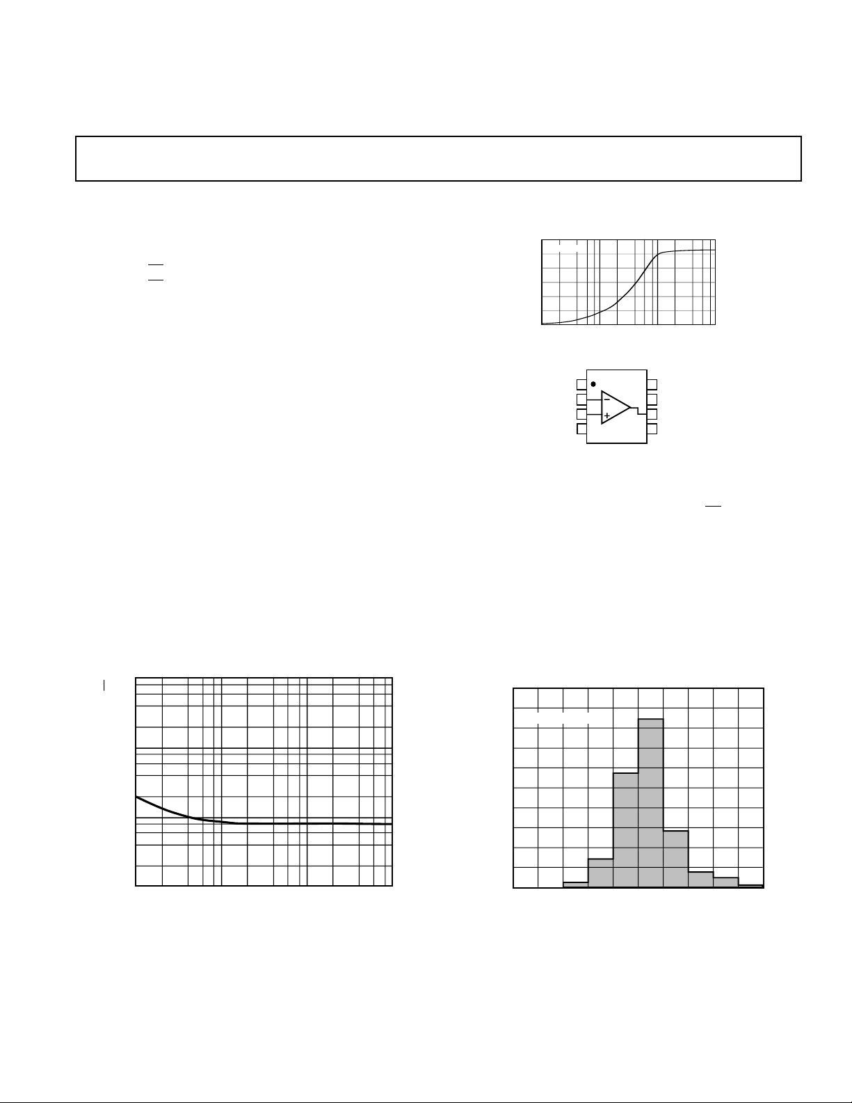
AD795
NC
–IN
+IN
–V
S
NC
+V
S
OUTPUT
NC
NC = NO CONNECT
Low Power, Low Noise
50
0
5–4
10
–5
30
20
40
43210–1–2–3
INPUT OFFSET VOLTAGE DRIFT – µV/°C
PERCENTAGE OF UNITS
SAMPLE SIZE = 570
a
FEATURES
Low Power Replacement for Burr-Brown
OPA-111, OPA-121 Op Amps
Low Noise
2.5 mV p-p max, 0.1 Hz to 10 Hz
11 nV/√
0.6 fA/√
High DC Accuracy
250 mV max Offset Voltage
3 mV/8C max Drift
1 pA max Input Bias Current
Low Power: 1.5 mA max Supply Current
Available in Low Cost Plastic Mini-DIP and Surface
Mount (SOIC) Packages
APPLICATIONS
Low Noise Photodiode Preamps
CT Scanners
Precision l-to-V Converters
PRODUCT DESCRIPTION
The AD795 is a low noise, precision, FET input operational
amplifier. It offers both the low voltage noise and low offset drift
of a bipolar input op amp and the very low bias current of a
FET-input device. The 10
insures that input bias current is essentially independent of
common-mode voltage and supply voltage variations.
The AD795 has both excellent dc performance and a guaranteed and tested maximum input voltage noise. It features 1 pA
maximum input bias current and 250 µV maximum offset volt-
age, along with low supply current of 1.5 mA max.
Hz max at 10 kHz
Hz at 1 kHz
1k
14
Ω common-mode impedance
Precision FET Op Amp
AD795
CONNECTION DIAGRAMS
8-Pin Plastic Mini-DIP (N) Package
30
Vs = ±15V
25
20
15
10
5
OUTPUT VOLTAGE SWING – Volts p-p
0
10
100 1k
LOAD RESISTANCE –
Ω
8-Pin SOIC (R) Package
Furthermore, the AD795 features a guaranteed low input noise
of 2.5 µV p-p (0.1 Hz to 10 Hz) and a 11 nV/√
level at 10 kHz. The AD795 has a fully specified and tested
input offset voltage drift of only 3 µV/°C max.
The AD795 is useful for many high input impedance, low noise
applications. The AD795J and AD795K are rated over the
commercial temperature range of 0°C to +70°C.
The AD795 is available in 8-pin plastic mini-DIP and 8-pin
surface mount (SOIC) packages.
10k
Hz max noise
REV. A
Information furnished by Analog Devices is believed to be accurate and
reliable. However, no responsibility is assumed by Analog Devices for its
use, nor for any infringements of patents or other rights of third parties
which may result from its use. No license is granted by implication or
otherwise under any patent or patent rights of Analog Devices.
100
10
VOLTAGE NOISE SPECTRAL DENSITY – nV/√Hz
1
10 100 10k1k
FREQUENCY – Hz
AD795 Voltage Noise Spectral Density
Typical Distribution of Average Input Offset Voltage Drift
One Technology Way, P.O. Box 9106, Norwood, MA 02062-9106, U.S.A.
Tel: 617/329-4700 Fax: 617/326-8703
Page 2

AD795–SPECIFICA TIONS
(@ +258C and 615 V dc unless otherwise noted)
AD795JN/JR AD795K
Parameter Conditions Min Typ Max Min Typ Max Units
INPUT OFFSET VOLTAGE
1
Initial Offset 100 500 50 250 µV
Offset T
MIN–TMAX
300 1000 100 400 µV
vs. Temperature 3 10 1 3 µV/°C
vs. Supply (PSRR) 86 110 90 110 dB
vs. Supply (PSRR) T
INPUT BIAS CURRENT
2
MIN–TMAX
84 100 87 100 dB
Either Input VCM = 0 V 1 2/3 1 1 pA
Either Input @ T
=V
MAX
Either Input V
Offset Current V
Offset Current @ T
=V
MAX
OPEN-LOOP GAIN V
= 0 V 23 23 pA
CM
= +10 V 1 1 pA
CM
= 0 V 0.1 1.0 0.1 0.6 pA
CM
= 0 V 2 2 pA
CM
= ±10 V
O
≥ 10 kΩ 110 120 110 120 dB
R
LOAD
R
≥ 10 kΩ 100 108 100 108 dB
LOAD
INPUT VOLTAGE NOISE 0.1 Hz to 10 Hz 1.0 3.3 1.0 2.5 µV p-p
f = 10 Hz 20 50 20 40 nV/√Hz
f = 100 Hz 12 40 12 30 nV/√
f = 1 kHz 11 17 11 15 nV/√
Hz
Hz
f = 10 kHz 9 11 9 11 nV/√Hz
INPUT CURRENT NOISE f = 0.1 Hz to 10 Hz 13 13 fA p-p
f = 1 kHz 0.6 0.6 fA/√Hz
FREQUENCY RESPONSE
Unity Gain, Small Signal G = –1 1.6 1.6 MHz
Full Power Response V
Slow Rate, Unity Gain V
SETTLING TIME
3
= 20 V p-p
O
R
= 2 kΩ 16 16 kHz
LOAD
= 20 V p-p
OUT
R
= 2 kΩ 11V/µs
LOAD
To 0.1% 10 V Step 10 10 µs
To 0.01% 10 V Step 11 11 µs
Overload Recovery
4
50% Overdrive 2 2 µs
Total Harmonic f = 1 kHz
Distortion R1 ≥ 10 kΩ
VO = 3 V rms –108 –108 dB
INPUT IMPEDANCE
Differential V
= ±1 V 1012i210
DIFF
12
i2 ΩipF
Common Mode 1014i2.2 1014i2.2 ΩipF
INPUT VOLTAGE RANGE
Differential
5
±20 ±20 V
Common-Mode Voltage ±10 ±11 ±10 ±11 V
Over Max Operating Temperature ±10 ±10 V
Common-Mode Rejection Ratio V
= ±10 V 90 110 94 110 dB
CM
T
MIN–TMAX
86 100 90 100 dB
OUTPUT CHARACTERISTICS
Voltage R
Current V
≥ 2 kΩ VS –4 VS –2.5 VS –4 VS –2.5 V
LOAD
T
MIN–TMAX
= ±10 V ± 5 ±10 ±5 ±10 mA
OUT
VS –4 VS –4 V
Short Circuit ±15 ±15 mA
POWER SUPPLY
Rated Performance ±15 ±15 V
Operating Range ±4 ±18 ±4 ±18 V
Quiescent Current 1.3 1.5 1.3 1.5 mA
–2–
REV. A
Page 3

AD795
NOTES
1
Input offset voltage specifications are guaranteed after 5 minutes of operation at TA = +25°C.
2
Bias current specifications are guaranteed maximum at either input after 5 minutes of operation at TA = +25°C. For higher temperature, the current doubles every 10°C.
3
Gain = –1, R1 = 10 kΩ.
4
Defined as the time required for the amplifier’s output to return to normal operation after removal of a 50% overload from the amplifier input.
5
Defined as the maximum continuous voltage between the inputs such that neither input exceeds ±10 V from ground.
All min and max specifications are guaranteed.
Specifications subject to change without notice.
ABSOLUTE MAXIMUM RATINGS
Supply Voltage . . . . . . . . . . . . . . . . . . . . . . . . . . . . . . . . ±18 V
Internal Power Dissipation
2
(@ TA = +25°C)
1
SOIC Package . . . . . . . . . . . . . . . . . . . . . . . . . . . . 500 mW
8-Pin Mini-DIP Package . . . . . . . . . . . . . . . . . . . . 750 mW
Input Voltage . . . . . . . . . . . . . . . . . . . . . . . . . . . . . . . . . . .±V
S
Output Short Circuit Duration . . . . . . . . . . . . . . . . Indefinite
Differential Input Voltage . . . . . . . . . . . . . . . . . . +V
and –V
S
S
Storage Temperature Range (N, R) . . . . . . . –65°C to +125°C
Operating Temperature Range
AD795J/K . . . . . . . . . . . . . . . . . . . . . . . . . . . 0°C to +70°C
NOTES
1
Stresses above those listed under “Absolute Maximum Ratings” may cause
permanent damage to the device. This is a stress rating only and functional
operation of the device at these or any other conditions above those indicated in the
operational section of this specification is not implied. Exposure to absolute
maximum rating conditions for extended periods may affect device reliability.
2
8-Pin Plastic Mini-DIP Package: θJA = 100°C/Watt
8-Pin Small Outline Package: θJA = 155°C/Watt
ESD SUSCEPTIBILITY
ESD (electrostatic discharge) sensitive device. Electrostatic
charges as high as 4000 volts, which readily accumulate on the
human body and on test equipment, can discharge without
detection. Although the AD795 features proprietary ESD protection circuitry, permanent damage may still occur on these
devices if they are subjected to high energy electrostatic discharges. Therefore, proper ESD precautions are recommended
to avoid any performance degradation or loss of functionality.
ORDERING GUIDE
Model Temperature Range Package Option*
AD795JN 0°C to +70°C N-8
AD795KN 0°C to +70°C N-8
AD795JR 0°C to +70°C R-8
*N = Plastic mini-DIP; R = SOIC package.
REV. A
–3–
Page 4
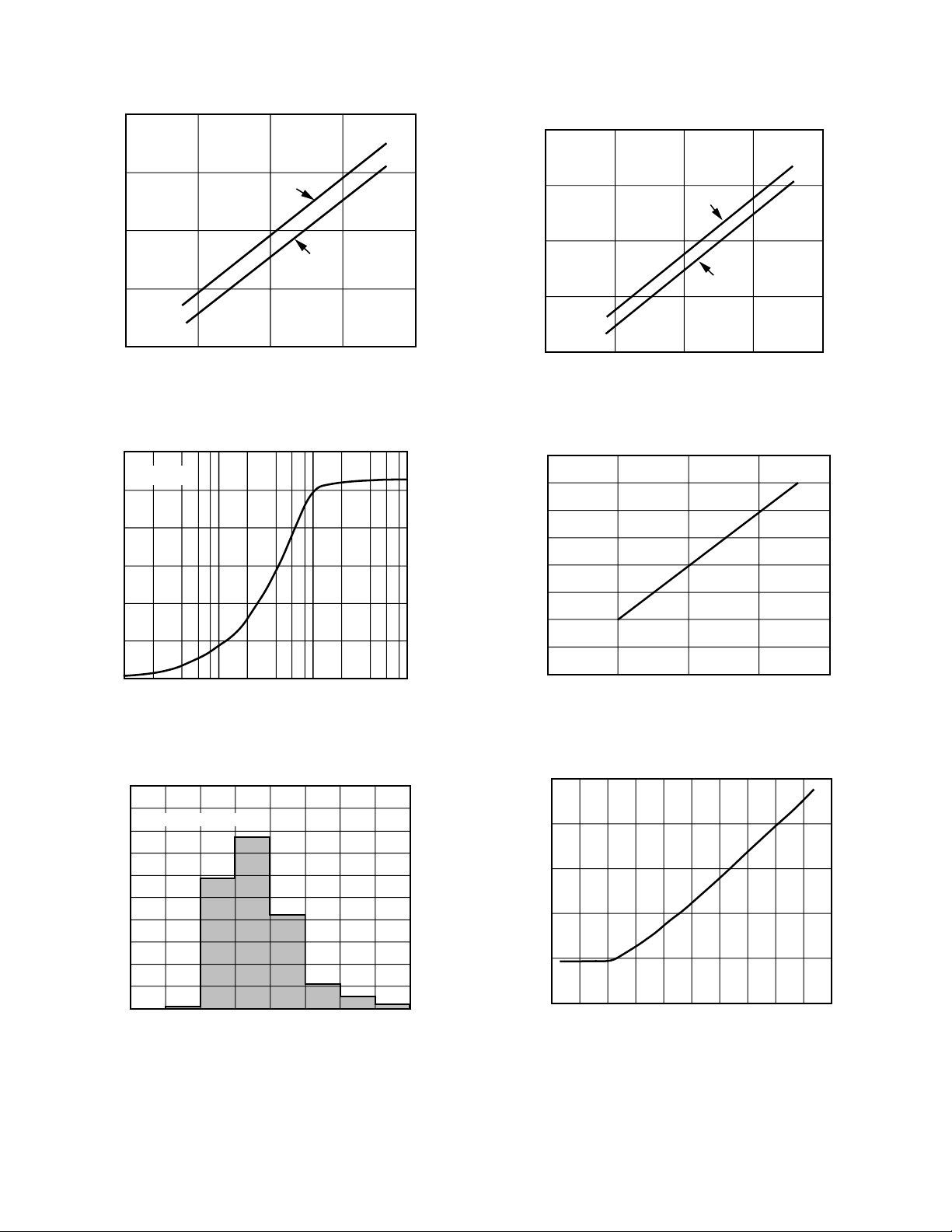
AD795–Typical Characteristics
OUTPUT VOLTAGE RANGE – ±Volts
SUPPLY VOLTAGE – ±Volts
20
0
020
15
5
5
10
10
15
R
L
= 10k
+V
OUT
–V
OUT
Ω
10
–9
10
–14
140
10
–11
10
–13
–40
10
–12
–60
10
–10
120100806040200–20
INPUT BIAS CURRENT – Amps
TEMPERATURE – °C
20
Ω
= 10k
R
L
15
+V
IN
10
–V
IN
5
INPUT COMMON MODE RANGE – ±Volts
0
020
5
10
15
SUPPLY VOLTAGE – ±Volts
Figure 1. Common-Mode Voltage Range vs. Supply
30
Vs = ±15V
25
20
15
10
5
OUTPUT VOLTAGE SWING – Volts p-p
Figure 2. Output Voltage Range vs. Supply Voltage
1.0
0.95
0.90
0.85
0.80
0.75
0.70
INPUT BIAS CURRENT – pA
0.65
0
10
100 1k
LOAD RESISTANCE –
Ω
10k
0.60
Figure 3. Output Voltage Swing vs. Load Resistance
50
SAMPLE SIZE = 1058
40
30
20
PERCENTAGE OF UNITS
10
0
0
INPUT BIAS CURRENT – pA
1.51.5
Figure 5. Typical Distribution of Input Bias Current
2
Figure 6. Input Bias Current vs. Temperature
0
5
SUPPLY VOLTAGE – ±Volts
1510
Figure 4. Input Bias Current vs. Supply
20
REV. A–4–
Page 5
VOLTAGE NOISE – µV p-p
SOURCE RESISTANCE – Ω
1k
10
1.0
10
3
10
4
10
9
10
8
10
7
10
6
10
5
Noise Bandwidth: 0.1 to 10Hz
100
FREQUENCY – Hz
1k
10
1.0
100
1 10 10M1M100k10k1k100
VOLTAGE NOISE (REFERRED TO INPUT) – nV/√Hz
1.00
0.95
0.90
0.85
0.80
0.75
0.70
INPUT BIAS CURRENT – pA
0.65
0.60
–10–15
–5
COMMON MODE VOLTAGE – Volts
0
+10+5
+15
Figure 7. Input Bias Current vs. Common-Mode Voltage
AD795
–4
10
–5
10
–I
IN
–6
10
–7
10
–8
10
–9
10
–10
10
–11
10
INPUT BIAS CURRENT – Amperes
–12
10
–13
10
–14
10
–5
–6
–4 –3
–2 –1
0
12
DIFFERENTIAL INPUT VOLTAGE – ±Volts
Figure 8. Input Bias Current vs. Differential Input Voltage
4
+I
IN
563
140
100
10
1.0
0.1
0.01
CURRENT NOISE – fA/√Hz
15
f = 1kHz
12.5
10
VOLTAGE NOISE – nV/√Hz
7.5
5
–60
–40
VOLTAGE NOISE
–20
CURRENT NOISE
100 120806040200
TEMPERATURE – °C
Figure 9. Voltage and Current Noise Spectral Density vs.
Temperature
50
SAMPLE SIZE = 344
40
f = 0.1 TO 10Hz
Figure 10. Input Voltage Noise vs. Source Resistance
30
20
PERCENTAGE OF UNITS
10
0
0
0.1 TO 10Hz INPUT VOLTAGE NOISE p-p – µV
21
Figure 11. Typical Distribution of Input Voltage Noise
REV. A
3
Figure 12. Input Voltage Noise Spectral Density
–5–
Page 6

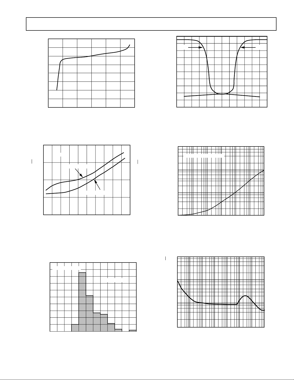
AD795–Typical Characteristics
10
–10
11
–4
–8
4
–6
3
2
–2
0
4
6
8
1098765
SETTING TIME – µs
OUTPUT SWING FROM 0 TO ±V
0.1%
0.01%
0.1% 0.01%
ERROR
120
–20
10M
40
0
100
20
10
100
60
80
1M100k10k1k
FREQUENCY – Hz
OPEN-LOOP GAIN – dB
PHASE MARGIN – Degrees
GAIN
PHASE
120
–20
40
0
20
100
60
80
30
25
– OUTPUT CURRENT
20
15
+ OUTPUT CURRENT
10
SHORT CIRCUIT CURRENT – mA
5
–40
–60
TEMPERATURE – °C
140
120100806040200–20
Figure 13. Short Circuit Current Limit vs. Temperature
1000
900
800
700
600
500
400
300
200
100
ABSOLUTE INPUT ERROR VOLTAGE – µV
0
–15
–10
INPUT COMMON MODE VOLTAGE – Volts
15
1050–5
Figure 15. Absolute Input Error Voltage vs. Input
Common-Mode Voltage
120
Figure 14. Output Swing and Error vs. Settling Time
120
100
80
60
40
20
POWER SUPPLY REJECTION – dB
0
1 10 10M1M100k10k1k100
–PSRR
FREQUENCY – Hz
+PSRR
Figure 16. Power Supply Rejection vs. Frequency
100
80
60
40
20
COMMON MODE REJECTION – dB
0
1 10 10M1M100k10k1k100
Figure 17. Common-Mode Rejection vs. Frequency
FREQUENCY – Hz
Figure 18. Open-Loop Gain & Phase Margin vs. Frequency
REV. A–6–
Page 7

AD795
QUIESCENT SUPPLY CURRENT – mA
20501510
SUPPLY VOLTAGE ± Volts
2.0
1.0
0.5
1.5
0
30
25
20
15
10
OUTPUT VOLTAGE – Volts p-p
5
0
1k
10k 100k 1M
FREQUENCY – Hz
RL = 10kΩ
Figure 19. Large Signal Frequency Response
–60
VIN = 3Vrms
R
= 10k
L
–70
–80
–90
THD – dB
–100
1000
100
10
1.0
CLOSED-LOOP OUTPUT IMPEDANCE – Ω
0.1
10k 10M1M100k1k
FREQUENCY – Hz
Figure 20. Closed-Loop Output Impedance vs. Frequency
–110
–120
100 1k 100k10k
FREQUENCY – Hz
Figure 21. Total Harmonic Distortion vs. Frequency
50
SAMPLE SIZE = 1419
40
30
20
PERCENTAGE OF UNITS
10
0
–500
INPUT OFFSET VOLTAGE – µV
Figure 23. Typical Distribution of Input Offset Voltage
Figure 22. Quiescent Supply Current vs. Supply
Voltage Drift
500–400
4003002001000–100–200–300
REV. A
–7–
Page 8

AD795
10
90
100
20mV
500ns
0%
10kΩ
V
IN
2
3
10kΩ
+V
7
AD795
4
–V
S
S
0.1µF
0.1µF
6
10kΩ
20V
100
90
V
OUT
R
L
C
L
100pF
10
0%
5V
5µs
100
90
10
0%
10mV
500ns
Figure 24. Unity Gain Inverter
Figure 25. Unity Gain Inverter
Large Signal Pulse Response
+V
S
0.1µF
7
2
0.1µF
6
10kΩ
R
L
V
IN
3
AD795
4
–V
S
Figure 27. Unity Gain Follower
C
L
100pF
100
90
V
OUT
10
0%
Figure 28. Unity Gain Follower
20V
5V
Large Signal Pulse Response
MINIMIZING INPUT CURRENT
The AD795 is guaranteed to 1 pA max input current with ±15
volt supply voltage at room temperature. Careful attention to
how the amplifier is used will maintain or possibly better this
performance.
The amplifier’s operating temperature should be kept as low as
possible. Like other JFET input amplifier’s, the AD795’s input
Figure 26. Unity Gain Inverter
Small Signal Pulse Response
5µs
Figure 29. Unity Gain Follower
Small Signal Pulse Response
current will double for every 10°C rise in junction temperature
(illustrated in Figure 6). On-chip power dissipation will raise the
device operating temperature, causing an increase in input
current. Reducing supply voltage to cut power dissipation will
reduce the AD795’s input current (Figure 4). Heavy output
loads can also increase chip temperature, maintaining a
minimum load resistance of 10 kΩ is recommended.
–8–
REV. A
Page 9

CIRCUIT BOARD NOTES
6
3
2
AD795
C
F
V
OUT
R
F
I
S
+
–
V
E
I
P
R
P
V
S
C
P
IP = + VS+ C
P
V
S
R
P
dC
P
dT
dV
S
dT
The AD795 is designed for throughhole mounting on PC
boards, using either mini-DIP or surface mount (SOIC).
Maintaining picoampere resolution in those environments
requires a lot of care. Both the board and the amplifier’s
package have finite resistance. Voltage differences between the
input pins and other pins as well as PC board metal traces will
cause parasitic currents (Figure 30) larger than the AD795’s
input current unless special precautions are taken. Two methods
of minimizing parasitic leakages are guarding of the input lines
and maintaining adequate insulation resistance.
Figures 31 and 32 show the recommended guarding schemes for
follower and inverted topologies. Note that for the mini-DIP,
the guard trace should be on both sides of the board. On the
SOIC, Pin 1 is not connected, and can be safely connected to
the guard. The high impedance input trace should be guarded
on both edges for its entire length.
GUARD TRACES PARALLEL
TO BOTH EDGES OF
INPUT TRACE
INPUT
TRACE
TO ANALOG
COMMON
–V
1
2
AD795
3
TOP VIEW
("N" PACKAGE)
S
4
8
7
6
5
Figure 30. Sources of Parasitic Leakage Currents
C
F
I
S
GUARD
2
3
AD795
R
F
6
+
V
OUT
–
AD795
8
BOTTOM
VIEW
7
PACKAGE)
6
5
("N"
1
2
3
4
1
2
3
TOP VIEW
("R" PACKAGE)
4
8
NOTE:
ON THE "R" PACKAGE
7
PINS 1, 5 AND 8 ARE OPEN
AND CAN BE CONNECTED
6
TO ANALOG COMMON OR
TO THE DRIVEN GUARD TO
5
REDUCE LEAKAGE.
Figure 31. Guarding Scheme–lnverter
GUARD TRACES
1
AD795
2
TOP VIEW
INPUT
TRACE
–V
3
4
S
Figure 32. Guard Scheme–Follower
8
7
6
5
CONNECT TO JUNCTION
OF RF AND RI, OR TO PIN 6
FOR UNITY GAIN.
GUARD
+
V
S
–
3
2
AD795
6
+
V
OUT
R
F
R
I
–
REV. A
–9–
Page 10

AD795
1
6
5
4
3
2
AD795
7
+V
S
V
OUT
100kΩ
–V
S
+
–
Leakage through the bulk of the circuit board will still occur
with the guarding schemes shown in Figures 31 and 32. Standard “G10” type printed circuit board material may not have
high enough volume resistivity to hold leakages at the subpicoampere level particularly under high humidity conditions.
One option that eliminates all effects of board resistance is
shown in Figure 33. The AD795’s sensitive input pin (either
Pin 2 when connected as an inverter, or Pin 3 when connected
as a follower) is bent up and soldered directly to a Teflon*
insulated standoff. Both the signal input and feedback component leads must also be insulated from the circuit board by
Teflon standoffs or low-leakage shielded cable.
INPUT PIN:
PIN 2 FOR INVERTER
OR PIN 3 FOR FOLLOWER
INPUT SIGNAL
PC
BOARD
LEAD
AD795
TEFLON INSULATED STANDOFF
1
2
AD795
3
4
8
7
6
5
Figure 33. Input Pin to Insulating Standoff
Contaminants such as solder flux on the board’s surface and on
the amplifier’s package can greatly reduce the insulation resistance between the input pin and those traces with supply or
signal voltages. Both the package and the board must be kept
clean and dry. An effective cleaning procedure is to first swab
the surface with high grade isopropyl alcohol, then rinse it with
deionized water and, finally, bake it at 100°C for 1 hour. Polypropylene and polystyrene capacitors should not be subjected to
the 100°C bake as they will be damaged at temperatures greater
than 80°C.
Other guidelines include making the circuit layout as compact
as possible and reducing the length of input lines. Keeping
circuit board components rigid and minimizing vibration will
reduce triboelectric and piezoelectric effects. All precision high
impedance circuitry requires shielding from electrical noise and
interference. For example, a ground plane should be used under
all high value (i.e., greater than 1 MΩ) feedback resistors. In
some cases, a shield placed over the resistors, or even the entire
amplifier, may be needed to minimize electrical interference
originating from other circuits. Referring to the equation in
Figure 30, this coupling can take place in either, or both, of two
different forms—coupling via time varying fields:
Both proper shielding and rigid mechanical mounting of
components help minimize error currents from both of these
sources.
OFFSET NULLING
The AD795’s input offset voltage can be nulled (mini-DIP
package only) by using balance Pins 1 and 5, as shown in
Figure 34. Nulling the input offset voltage in this fashion will
introduce an added input offset voltage drift component of
2.4 µV/°C per millivolt of nulled offset.
Figure 34. Standard Offset Null Circuit
The circuit in Figure 35 can be used when the amplifier is used
as an inverter. This method introduces a small voltage in series
with the amplifier’s positive input terminal. The amplifier’s
input offset voltage drift with temperature is not affected.
However, variation of the power supply voltages will cause
offset shifts.
R
AD795
499kΩ
F
6
+V
–V
S
100kΩ
S
+
V
OUT
–
R
I
+
V
I
–
2
3
499kΩ
200Ω 0.1µF
Figure 35. Alternate Offset Null Circuit for Inverter
dV
C
P
dT
or by injection of parasitic currents by changes in capacitance
due to mechanical vibration:
*Teflon is a registered trademark of E.I. du Pont Co.
dCp
V
dT
–10–
REV. A
Page 11

AC RESPONSE WITH HIGH VALUE SOURCE AND
10
90
100
10mV
5µs
0%
FEEDBACK RESISTANCE
Source and feedback resistances greater than 100 kΩ will
magnify the effect of input capacitances (stray and inherent to
the AD795) on the ac behavior of the circuit. The effects of
common-mode and differential input capacitances should be
taken into account since the circuit’s bandwidth and stability
can be adversely affected.
In a follower, the source resistance, R
mode capacitance, C
(including capacitance due to board and
S
, and input common-
S
capacitance inherent to the AD795), form a pole that limits
circuit bandwidth to 1/2 π R
. Figure 36 shows the follower
SCS
pulse response from a 1 MΩ source resistance with the
amplifier’s input pin isolated from the board, only the effect of
the AD795’s input common-mode capacitance is seen.
10mV
100
90
10
0%
Figure 36. Follower Pulse Response from 1 M
5µs
Ω
Source Resistance
In an inverting configuration, the differential input capacitance
forms a pole in the circuit’s loop transmission. This can create
peaking in the ac response and possible instability. A feedback
capacitance can be used to stabilize the circuit. The inverter
pulse response with R
and RS equal to 1 MΩ, and the input pin
F
isolated from the board appears in Figure 37. Figure 38 shows
the response of the same circuit with a 1 pF feedback
capacitance. Typical differential input capacitance for the
AD795 is 2 pF.
10mV
100
90
5µs
AD795
Figure 38. Inverter Pulse Response with 1 MΩ Source and
Feedback Resistance, 1 pF Feedback Capacitance
OVERLOAD ISSUES
Driving the amplifier output beyond its linear region causes
some sticking; recovery to normal operation is within 2 µs of the
input voltage returning within the linear range.
If either input is driven below the negative supply, the amplifier’s
output will be driven high, causing a phenomenon called phase
reversal. Normal operation is resumed within 30 µs of the input
voltage returning within the linear range.
Figure 39 shows the AD795’s input currents versus differential
input voltage. Picoamp level input current is maintained for
differential voltages up to several hundred millivolts. This
behavior is only important if the AD795 is in an open-loop
application where substantial differential voltages are produced.
–4
10
–5
10
–I
N
–6
10
–7
10
–8
10
–9
10
–10
10
–11
10
–12
10
INPUT BIAS CURRENT – Amperes
–13
10
–14
10
–6 –5 –4 –3 –2 –1 0 1 2 3 4 5 6
DIFFERENTIAL INPUT VOLTAGE – ±Volts
+I
N
Figure 39. Input Bias Current vs. Differential Input Voltage
10
0%
Figure 37. Inverter Pulse Response with 1 MΩ Source and
Feedback Resistance
REV. A
–11–
Page 12

AD795
6
3
2
SOURCE
AD795
R
F
PROTECT DIODES
(LOW LEAKAGE)
INPUT PROTECTION
The AD795 safely handles any input voltage within the supply
voltage range. Some applications may subject the input
terminals to voltages beyond the supply voltages—in these
cases, the following guidelines should be used to maintain the
AD795’s functionality and performance.
If the inputs are driven more than a 0.5 V below the minus supply, milliamp level currents can be produced through the input
terminals. That current should be limited to 10 mA for “transient” overloads (less than 1 second) and 1 mA for continuous
overloads, this can be accomplished with a protection resistor in
the input terminal (as shown in Figures 40 and 41). The protection resistor’s Johnson noise will add to the amplifier’s input
voltage noise and impact the frequency response.
Driving the input terminals above the positive supply will cause
the input current to increase and limit at 40 µA. This condition
is maintained until 15 volts above the positive supply—any
input voltage within this range does not harm the amplifier.
Input voltage above this range causes destructive breakdown
and should be avoided.
R
F
R
SOURCE
P
3
2
AD795
6
Figure 41. Follower with Input Current Limit
Figure 42 is a schematic of the AD795 as an inverter with an
input voltage clamp. Bootstrapping the clamp diodes at the
inverting input minimizes the voltage across the clamps and
keeps the leakage due to the diodes low. Low leakage diodes
(less than 1 pA), such as the FD333s should be used, and
should be shielded from light to keep photocurrents from being
generated. Even with these precautions, the diodes will measurably increase the input current and capacitance.
In order to achieve the low input bias currents of the AD795, it
is not possible to use the same on-chip protection as used in
other Analog Devices op amps. This makes the AD795
sensitive to handling and precautions should be taken to
minimize ESD exposure whenever possible.
C
SOURCE
R
P
2
3
AD795
F
6
Figure 40. Inverter with Input Current Limit
Figure 42. Input Voltage Clamp with Diodes
–12–
REV. A
Page 13

AD795
10pF
9
10 Ω
GUARD
PHOTODIODE
2
AD795
3
8
6
OPTIONAL 26Hz
OUTPUT
FILTER
FILTERED
OUTPUT
Figure 43. The AD795 Used as a Photodiode Preamplifier
Preamplifier Applications
The low input current and offset voltage levels of the AD795
together with its low voltage noise make this amplifier an
excellent choice for preamplifiers used in sensitive photodiode
applications. In a typical preamp circuit, shown in Figure 43,
the output of the amplifier is equal to:
V
= ID (Rf) = Rp (P) Rf
OUT
where:
= photodiode signal current (Amps)
I
D
Rp = photodiode sensitivity (Amp/Watt)
Rf = the value of the feedback resistor, in ohms.
P = light power incident to photodiode surface, in watts.
An equivalent model for a photodiode and its dc error sources is
shown in Figure 44. The amplifier’s input current, I
, will
B
contribute an output voltage error which will be proportional to
the value of the feedback resistor. The offset voltage error, V
OS
,
will cause a “dark” current error due to the photodiode’s finite
shunt resistance, Rd. The resulting output voltage error, V
, is
E
equal to:
V
= (1 + Rf/Rd) VOS + Rf I
E
B
A shunt resistance on the order of 109 ohms is typical for a
small photodiode. Resistance Rd is a junction resistance which
Cf
10pF
Rf
9
10 Ω
PHOTODIODE
Rd
Cd
I
D
50pF
V
OS
I
B
OUTPUT
will typically drop by a factor of two for every 10°C rise in
temperature. In the AD795, both the offset voltage and drift are
low, this helps minimize these errors.
Minimizing Noise Contributions
The noise level limits the resolution obtainable from any preamplifier. The total output voltage noise divided by the
feedback resistance of the op amp defines the minimum
detectable signal current. The minimum detectable current
divided by the photodiode sensitivity is the minimum detectable
light power.
Sources of noise in a typical preamp are shown in Figure 45.
The total noise contribution is defined as:
OUTPUT
2
V
OUT
= (i
iSRd
2
2
+
i
+i
f
n
PHOTODIODE
s
2
)
1+ s(Cf ) Rf
i
S
Rf
Cd
50pF
2
2
+(en
)
en
i
n
1+
10pF
Rf
Rd
Cf
1+ s(Cd) Rd
1+ s(Cf ) Rf
Rf
9
10 Ω
i
f
Figure 45. Noise Contributions of Various Sources
Figure 46, a spectral density versus frequency plot of each
source’s noise contribution, shows that the bandwidth of the
amplifier’s input voltage noise contribution is much greater than
its signal bandwidth. In addition, capacitance at the summing
junction results in a “peaking” of noise gain in this configuration. This effect can be substantial when large photodiodes with
large shunt capacitances are used. Capacitor Cf sets the signal
bandwidth and also limits the peak in the noise gain. Each
source’s rms or root-sum-square contribution to noise is obtained by integrating the sum of the squares of all the noise
sources and then by obtaining the square root of this sum.
Minimizing the total area under these curves will optimize the
preamplifier’s overall noise performance.
An output filter with a passband close to that of the signal can
greatly improve the preamplifier’s signal to noise ratio. The
photodiode preamplifier shown in Figure 45—without a
bandpass filter—has a total output noise of 50 µV rms. Using a
26 Hz single pole output filter, the total output noise drops to
23 µV rms, a factor of 2 improvement with no loss in signal
bandwidth.
Figure 44. A Photodiode Model Showing DC Error
Sources
REV. A
–13–
Page 14

AD795
GUARD
AD795
–V
S
V ADJUST
100kΩ
OS
PH
PROBE
+V
S
OUTPUT
1VOLT/pH UNIT
19.6kΩ
RT
1kΩ
+3500ppm/ °C
0.1µF
0.1µF
+15V
COM
–15V
–V
S
+V
S
1
3
2
4
5
6
7
8
10µV
&
i
i
s
Hz
√
1µV
100nV
e
n
OUTPUT VOLTAGE NOISE – Volts/
10nV
f
SIGNAL BANDWIDTH
i
n
en
100 1k 10k 100k101
FREQUENCY – Hz
WITH FILTER
NO FILTER
Figure 46. Voltage Noise Spectral Density of the Circuit of
Figure 45 With and Without an Output Filter
PHOTODIODE
10pF
Rf
8
10 Ω
AD795
R
G
10kΩ
R
i
1.1kΩ
R
V = I Rf (1+ )
OUT D
G
R
V
OUT
i
voltage contributions are also amplified by the “T” network
gain. A low noise, low offset voltage amplifier, such as the
AD795, is needed for this type of application.
A pH Probe Buffer Amplifier
A typical pH probe requires a buffer amplifier to isolate its 10
6
to 109 Ω source resistance from external circuitry. Just such an
amplifier is shown in Figure 48. The low input current of the
AD795 allows the voltage error produced by the bias current
and electrode resistance to be minimal. The use of guarding,
shielding, high insulation resistance standoffs, and other such
standard methods used to minimize leakage are all needed to
maintain the accuracy of this circuit.
The slope of the pH probe transfer function, 50 mV per pH
unit at room temperature, has a +3300 ppm/°C temperature
coefficient. The buffer of Figure 48 provides an output voltage
equal to 1 volt/pH unit. Temperature compensation is provided
by resistor RT which is a special temperature compensation
resistor, part number Q81, 1 kΩ, 1%, +3500 ppm/°C, available
from Tel Labs Inc.
Figure 47. A Photodiode Preamp Employing a “T”
Network for Added Gain
Using a “T” Network
A “T” network, shown in Figure 47, can be used to boost the
effective transimpedance of an I-to-V converter, for a given
feedback resistor value. However, amplifier noise and offset
Figure 48. A pH Probe Amplifier
–14–
REV. A
Page 15

LOW NOISE
OP AMPS
AD795
Audio
Amplifiers
OP275
SSM2015
SSM2016
SSM2017
SSM2134
SSM2139
Low V
(V
≤ 10 nV/√Hz @ 1 kHz)
N
Fast
(SR ≥ 45 V/µs)
OP61
Faster
(SR ≥ 230 V/µs)
AD5539
AD829
AD840
AD844
AD846
AD848
AD849
Ultrafast
(SR ≥ 1000 V/µs)
AD811
AD844
AD9610
AD9617
AD9618
N
Precision
AD OP27
OP27
AD OP37
OP37
OP227 (Dual)
OP270 (Dual)
OP271 (Dual)
OP470 (Quad)
OP471 (Quad)
High Output
Current
OP50
(IN ≤ 10 fA/√Hz @ 1 kHz)
FET Input
AD645
AD743
AD795
Fast
AD745
Low Power
AD548
AD648
OP80
Faster
(SR ≥ 8 V/µs)
OP282 (Dual)
OP482 (Quad)
Low Noise Op Amp Selection Tree
Low I
Fast
AD711
AD712 (Dual)
OP249 (Dual)
AD713 (Quad)
Faster
AD744
OP42
OP44
AD746 (Dual)
N
Low VN
AD645
AD795
Lower V
AD743
Faster
AD745
N
Electrometer
Low
Power
OP80
General
Purpose
AD546
Lowest I
60 fA Max
AD549
B
REV. A
–15–
Page 16

AD795
OUTLINE DIMENSIONS
Dimensions shown in inches and (mm).
Plastic Mini-DIP (N) Package
0.244 (6.20)
0.228 (5.79)
PIN 1
0.010 (0.25)
0.004 (0.10)
8
PIN 1
1
0.39 (9.91) MAX
0.165±0.01
(4.19±0.25)
0.125
(3.18)
MIN
0.10
0.018±0.003
(0.46±0.08)
(2.54)
BSC
0.033
(0.84)
NOM
8-Pin SOIC (R) Package
0.150 (3.81)
8
1
0.197 (5.01)
0.189 (4.80)
0.050
(1.27)
BSC
5
4
0.019 (0.48)
0.014 (0.36)
0.157 (3.99)
0.150 (3.81)
0.102 (2.59)
0.094 (2.39)
0.098 (0.2482)
0.075 (0.1905)
5
0.25
(6.35)
4
0.035±0.01
(0.89±0.25)
0.18±0.03
(4.57±0.76)
SEATING
PLANE
0.020 (0.051) x 45
CHAMF
8
°
0
°
0.31
(7.87)
°
0.190 (4.82)
0.170 (4.32)
10
°
0
°
0.30 (7.62)
REF
0.011±0.003
(0.28±0.08)
15
°
0
°
0.030 (0.76)
0.018 (0.46)
0.090
(2.29)
C1712–24–10/92
All brand or product names mentioned are trademarks or registered trademarks of their respective holders.
–16–
PRINTED IN U.S.A.
REV. A
 Loading...