

Page 1
LC2MOS
a
FEATURES
Two 12-Bit DACs in One Package
DAC Ladder Resistance Matching: 0.5%
Surface-Mount Package
4-Quadrant Multiplication
Low Gain Error (3 LSB max Over Temperature)
Byte Loading Structure
Fast Interface Timing
APPLICATIONS
Automatic Test Equipment
Programmable Filters
Audio Applications
Synchro Applications
Process Control
GENERAL DESCRIPTION
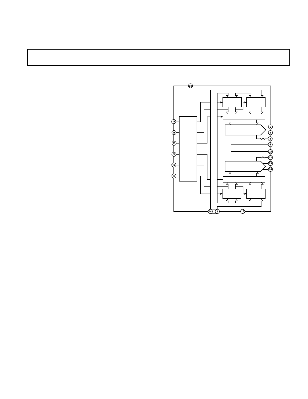
The AD7937 contains two 12-bit current output DACs on one
monolithic chip. A separate reference input is provided for each
DAC. The dual DAC saves valuable board space, and the monolithic construction ensures excellent thermal tracking. Both DACs
are guaranteed 12-bit monotonic over the full temperature range.
The AD7937 has a 2-byte (eight LSBs, four MSBs) loading
structure. It is designed for right-justified data format. The control
signals for register loading are A0, A1, CS, WR, and UPD. Data
is loaded to the input registers when CS and WR are low. To
transfer this data to the DAC registers, UPD must be taken
low with WR.
Added features on the AD7937 include an asynchronous CLR
line which is very useful in calibration routines. When this is
taken low, all registers are cleared. The double buffering of the
data inputs allows simultaneous update of both DACs. Also,
each DAC has a separate AGND line. This increases the device
versatility; for instance, one DAC may be operated with AGND
biased while the other is connected in the standard configuration.
The AD7937 is manufactured using the Linear Compatible
CMOS (LC
microprocessors and accepts TTL, 74HC, and 5 V CMOS logic
level inputs.
2
MOS) process. It is speed compatible with most
(8+4) Loading Dual 12-Bit DAC
AD7937
FUNCTIONAL BLOCK DIAGRAM
V
DD
AD7937
UPD
A1
A0
CONTROL
CS
WR
CLR
LOGIC
DB7–DB0 DGND
PRODUCT HIGHLIGHTS
1. DAC-to-DAC Matching
Since both DACs are fabricated on the same chip, precise
matching and tracking is inherent. Many applications that are
not practical using two discrete DACs are now possible.
Typical matching: 0.5%.
2. Small Package Size
The AD7937 is packaged in a small 24-lead SOIC.
3. Wide Power Supply Tolerance
The device operates on a 5 V V
this nominal figure. All specifications are guaranteed over
this range.
DAC A MS
INPUT REG
48
DAC A REGISTER
DAC B REGISTER
48
DAC B MS
INPUT REG
DD
DAC A LS
INPUT REG
12
DAC A
DAC B
12
DAC B LS
INPUT REG
, with ±10% tolerance on
I
OUTA
AGNDA
R
FBA
V
REFA
V
REFB
R
FBB
I
OUTB
AGNDB
REV. 0
Information furnished by Analog Devices is believed to be accurate and
reliable. However, no responsibility is assumed by Analog Devices for its
use, nor for any infringements of patents or other rights of third parties
which may result from its use. No license is granted by implication or
otherwise under any patent or patent rights of Analog Devices.
One Technology Way, P.O. Box 9106, Norwood, MA 02062-9106, U.S.A.
Tel: 781/329-4700 World Wide Web Site: http://www.analog.com
Fax: 781/326-8703 © Analog Devices, Inc., 2000
Page 2
AD7937–SPECIFICATIONS
(VDD = 5 V 10%, V
specifications T
MIN
= V
REFA
to T
MAX
= 10 V; I
REFB
unless otherwise noted.)
= AGNDA = 0 V, I
OUTA
= AGNDB = 0 V. All
OUTB
Parameter A Version B Version Unit Test Conditions/Comments
ACCURACY
Resolution 12 12 Bits
Relative Accuracy ±1 ±1/2 LSB max
Differential Nonlinearity ±1 ±1 LSB max All grades guaranteed monotonic over temperature.
, R
Gain Error ±6 ±3 LSB max Measured using R
Gain Temperature Coefficient
2
;
. Both DAC registers loaded with all 1s.
FBA
FBB
∆Gain/∆Temperature ±5 ±5 ppm/°C max Typical value is 1 ppm/°C.
Output Leakage Current
I
OUTA
I
OUTB
5 5 nA max DAC A Register loaded with all 0s.
10 10 nA max
5 5 nA max DAC B Register loaded with all 0s.
10 10 nA max
REFERENCE INPUT
Input Resistance 9 9 kΩ min Typical Input Resistance = 14 kΩ.
20 20 kΩ max
, V
V
REFA
REFB
Input Resistance Match ±3 ±3 % max Typically ±0.5%.
DIGITAL INPUTS
(Input High Voltage) 2.4 2.4 V min
V
IH
(Input Low Voltage) 0.8 0.8 V max
V
IL
(Input Current)
I
IN
+25°C ±1 ±1 µA max V
to T
T
MIN
CIN (Input Capacitance)
MAX
2
±10 ± 10 µA max
10 10 pF max
= VDD.
IN
POWER SUPPLY
V
DD
I
DD
4.5/5.5 4.5/5.5 V min/V max
2 2 mA max
0.1 0.1 mA typ
AC PERFORMANCE CHARACTERISTICS
These characteristics are included for Design Guidance only and are not subject to test.
(VDD = 5 V; V
Parameter TA = 25C Unit Test Conditions/Comments
Output Current Settling Time 1 µs max To 0.01% of full-scale range. I
Digital-to-Analog Glitch lmpulse 2.5 nV-s typ Measured with V
AC Feedthrough
V
REFA
V
REFB
Power Supply Rejection
∆Gain/∆V
Output Capacitance
C
OUTA
C
OUTB
C
OUTA
C
OUTB
Channel-to-Channel Isolation
V
REFA
V
REFB
Digital Crosstalk 2.5 nV-s typ Measured for a Code Transition of all 0s to all 1s. I
Output Noise Voltage Density 25 nV/√Hz typ Measured between R
(10 Hz–100 kHz) is 10 Hz–100 kHz.
Total Harmonic Distortion –82 dB typ VIN = 6 V rms, 1 kHz. Both DACs loaded with all 1s.
NOTES
1
Temperature range as follows: A, B Versions: –40°C to +85°C.
2
Sample tested at 25°C to ensure compliance.
Specifications subject to change without notice.
to I
to I
to I
to I
REFA
OUTA
OUTB
DD
OUTB
OUTA
= V
= 10 V; I
REFB
= AGNDA = 0 V, I
OUTA
–70 dB max V
–70 dB max DAC registers loaded with all 0s.
= AGNDB = 0 V. Output Amplifiers are AD644 except where noted.)
OUTB
load = 100 Ω, C
REFB
OUT
= 0 V. I
measured from falling edge of WR. Typical Value of Settling Time is 0.6 µs.
= V
registers alternately loaded with all 0s and all 1s.
, V
REFA
REFA
= 20 V p-p 10 kHz sine wave.
REFB
±0.01 % per % max ∆VDD = VDD max – VDD min.
70 pF max DAC A, DAC B loaded with all 0s.
70 pF max
140 pF max DAC A, DAC B loaded with all 1s.
140 pF max
–84 dB typ V
–84 dB typ V
= 20 V p-p 10 kHz sine wave, V
REFA
= 20 V p-p 10 kHz sine wave, V
REFB
C
= 13 pF.
EXT
and I
FBA
OUTA
EXT
, I
load = 100 Ω, C
OUTB
= 0 V. Both DACs loaded with all 1s.
= 0 V. Both DACs loaded with all 1s.
OUTA
and I
. Frequency of measurement
OUTB
or R
OUTA
REFB
REFA
FBB
= 13 pF. DAC output
= 13 pF. DAC
EXT
, I
load = 100 Ω,
OUTB
–2–
REV. 0
Page 3
AD7937
WARNING!
ESD SENSITIVE DEVICE
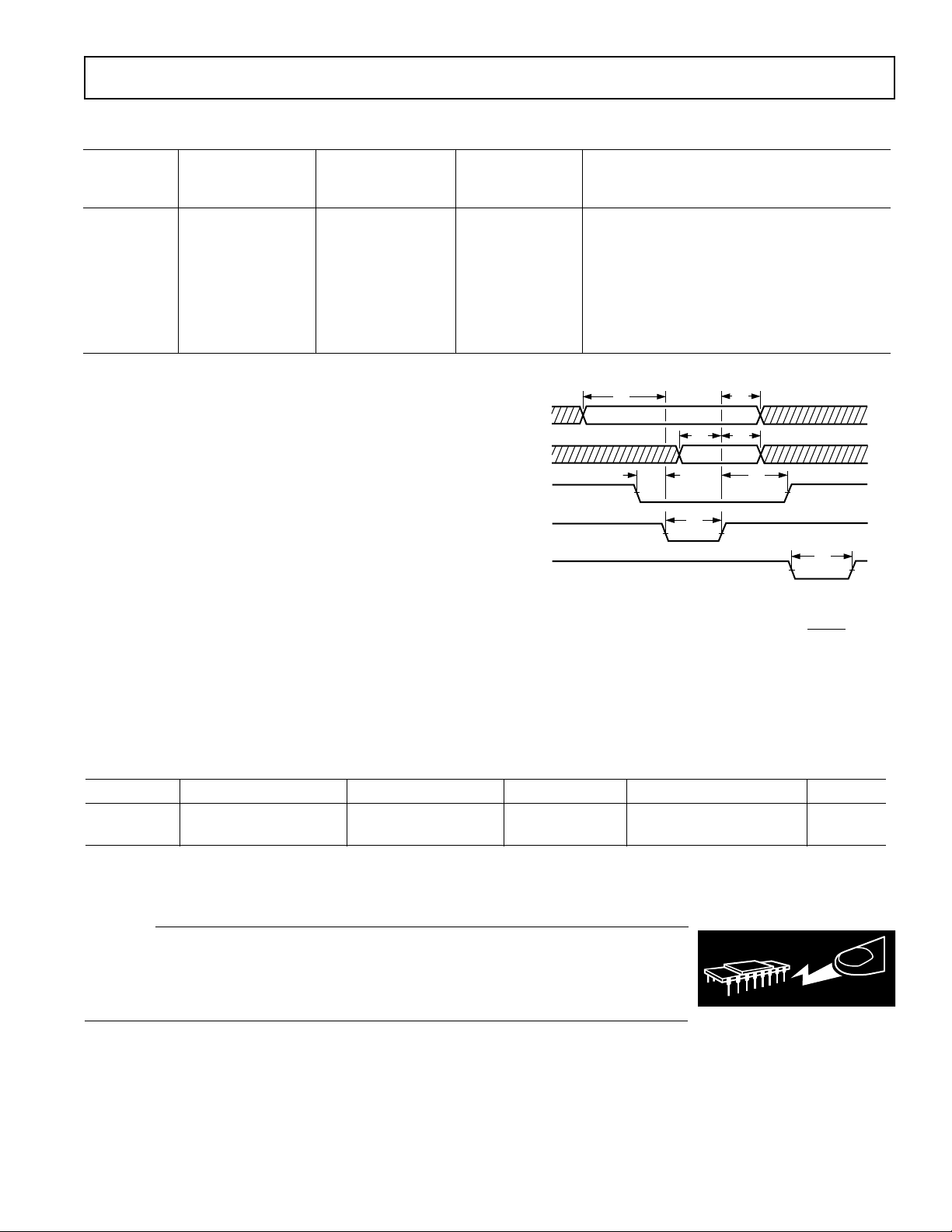
TIMING CHARACTERISTICS
(VDD = 5 V 10%, V
REFA
= V
= 10 V; I
REFB
= AGNDA = 0 V, I
OUTA
= AGNDB = 0 V.)
OUTB
Limit at
Limit at T
= –40C
A
Parameter TA = 25C to +85C Unit Test Conditions/Comments
t
1
t
2
t
3
t
4
t
5
t
6
t
7
t
8
Specifications subject to change without notice.
ABSOLUTE MAXIMUM RATINGS*
(TA = 25°C unless otherwise noted)
VDD to DGND . . . . . . . . . . . . . . . . . . . . . . . . . . –0.3 V, +17 V
, V
V
V
REFA
RFBA
to AGNDA, AGNDB . . . . . . . . . . . . . . . . ±25 V
REFB
, V
to AGNDA, AGNDB . . . . . . . . . . . . . . . . ±25 V
RFBB
Digital Input Voltage to DGND . . . . . . . –0.3 V, V
, I
I
OUTA
to DGND . . . . . . . . . . . . . . –0.3 V, VDD +0.3 V
OUTB
AGNDA, AGNDB to DGND . . . . . . . . . –0.3 V, V
SOIC Package
, Thermal Impedance . . . . . . . . . . . . . . . . . . . . 72°C/W
θ
JA
Lead Temperature (Soldering, 10 sec) . . . . . . . . . . . . 300°C
IR Ref Low Peak Temperature . . . . . . . . . . . . . . . . . . 220°C
Operating Temperature Range
Industrial (A, B Versions) . . . . . . . . . . . . . –40°C to +85°C
10 10 ns min Address Valid to Write Setup Time
10 10 ns min Address Valid to Write Hold Time
20 40 ns min Data Setup Time
30 30 ns min Data Hold Time
0 0 ns min Chip Select or Update to Write Setup Time
0 0 ns min Chip Select or Update to Write Hold Time
115 125 ns min Write Pulsewidth
90 100 ns min Clear Pulsewidth
t
3
t
7
t
2
t
4
= tf = 20ns.
r
t
6
+0.3 V
DD
+0.3 V
DD
A0–A1
DATA
CS, UPD
WR
CLR
t
1
t
5
NOTES
1. ALL INPUT SIGNAL RISE AND FALL TIMES MEASURED
FROM 10% TO 90% OF +5V. t
2. TIMING MEASUREMENT REFERENCE LEVELS IS
Storage Temperature . . . . . . . . . . . . . . . . –65°C to +150°C
*Stresses above those listed under Absolute Maximum Ratings may cause perma-
nent damage to the device. This is a stress rating only; functional operation of the
device at these or any other conditions above those indicated in the operational
sections of this specification is not implied. Exposure to absolute maximum rating
conditions for extended periods may affect device reliability.
Figure 1. Timing Diagram
5V
0V
5V
0V
5V
0V
5V
0V
t
8
+ V
V
IH
5V
0V
IL
2
ORDERING GUIDE
Model Temperature Range Relative Accuracy Gain Error Package Description Option
AD7937AR –40°C to +85°C ±1 LSB ±6 LSB Small Outline R-24
AD7937BR –40°C to +85°C ± 1/2 LSB ±3 LSB Small Outline R-24
CAUTION
ESD (electrostatic discharge) sensitive device. Electrostatic charges as high as 4000 V readily
accumulate on the human body and test equipment and can discharge without detection. Although
the AD7937 features proprietary ESD protection circuitry, permanent damage may occur on
devices subjected to high-energy electrostatic discharges. Therefore, proper ESD precautions are
recommended to avoid performance degradation or loss of functionality.
REV. 0
–3–
Page 4

AD7937
PIN FUNCTION DESCRIPTIONS
Pin Mnemonic Description
1 AGNDA Analog Ground for DAC A.
2I
3R
4V
OUTA
FBA
REFA
Current output terminal of DAC A.
Feedback resistor for DAC A.
Reference input to DAC A.
5 CS Chip Select Input Active low.
6–11 DB0–DB7 Eight data inputs, DB0–DB7.
13, 14
12 DGND Digital Ground.
15 A0 Address Line 0.
16 A1 Address Line 1.
17 CLR Clear Input. Active low. Clears all
registers.
18 WR Write Input. Active low.
19 UPD Updates DAC Registers from inputs
registers.
20 V
DD
Power supply input. Nominally 5 V to
15 V, with ±10% tolerance.
21 V
22 R
23 I
REFB
FBB
OUTB
Reference input to DAC B.
Feedback resistor for DAC B.
Current output terminal of DAC B.
24 AGNDB Analog Ground for DAC B.
PIN CONFIGURATION
SOIC
AGNDA
I
OUTA
R
FBA
V
REFA
CS
DB0
DB1
DB2
DB3
DB4
DB5
DGND
1
2
3
4
5
AD7937
6
TOP VIEW
(Not to Scale)
7
8
9
10
11
12
24
23
22
21
20
19
18
17
16
15
14
13
AGNDB
I
OUTB
R
FBB
V
REFB
V
DD
UPD
WR
CLR
A1
A0
DB7
DB6
CIRCUIT INFORMATION – D/A SECTION
The AD7937 contains two identical 12-bit multiplying D/A
converters. Each DAC consists of a highly stable R-2R ladder
and 12 N-channel current steering switches. Figure 2 shows a
simplified D/A circuit for DAC A. In the R-2R ladder, binary
weighted currents are steered between I
and AGNDA. The
OUTA
current flowing in each ladder leg is constant, irrespective of
switch state. The feedback resistor R
(see Figures 4 and 5) to convert the current flowing in I
is used with an op amp
FBA
OUTA
to
a voltage output.
V
REFA
R
2R
S112RS10
R
2R
2R
R
S0
FBA
R
I
OUTA
AGNDA
Figure 2. Simplified Circuit Diagram for DAC A
EQUIVALENT CIRCUIT ANALYSIS
Figure 3 shows the equivalent circuit for one of the D/A converters (DAC A) in the AD7937. A similar equivalent circuit
can be drawn for DAC B.
V
REFA
R
D.V
REF
R
R
I
O
R
LKG
R
FBA
I
OUTA
C
OUT
AGNDA
Figure 3. Equivalent Analog Circuit for DAC A
C
is the output capacitance due to the N-channel switches
OUT
and varies from about 50 pF to 100 pF with digital input code.
The current source I
leakages and approximately doubles every 10°C. R
is composed of surface and junction
LKG
is the equiva-
O
lent output resistance of the device which varies with input code.
DIGITAL CIRCUIT INFORMATION
The digital inputs are designed to be both TTL and 5 V CMOS
compatible. All logic inputs are static protected MOS gates with
typical input currents of less than 1 nA.
Table I. AD7937 Truth Table
CLR UPD CS WR A1 A0 Function
1 1 1 X X X No Data Transfer
1 1 X 1 X X No Data Transfer
0 X X X X X All Registers Cleared
1 1 0 0 0 0 DAC A LS Input Register
Loaded with DB7–DB0 (LSB)
1 1 0 0 0 1 DAC A MS Input Register
Loaded with DB3 (MSB)–DB0
1 1 0 0 1 0 DAC B LS Input Register
Loaded with DB7–DB0 (LSB)
1 1 0 0 1 1 DAC B MS Input Register
Loaded with DB3 (MSB)–DB0
1 0 1 0 X X DAC A, DAC B Registers
Updated Simultaneously from
Input Registers
1 0 0 0 X X DAC A, DAC B Registers are
Transparent
NOTE: X = Don’t care
–4–
REV. 0
Page 5

AD7937
UNIPOLAR BINARY OPERATION
(2-QUADRANT MULTIPLICATION)
Figure 4 shows the circuit diagram for unipolar binary operation.
With an ac input, the circuit performs 2-quadrant multiplication.
The code table for Figure 4 is given in Table II.
Operational amplifiers A1 and A2 can be in a single package
(AD644, AD712) or separate packages (AD544, AD711,
AD OP27). Capacitors C1 and C2 provide phase compensation
to help prevent overshoot and ringing when high-speed op amps
are used.
For zero offset adjustment, the appropriate DAC register is loaded
with all 0s and amplifier offset adjusted so that V
OUTA
or V
OUTB
is 0 V. Full-scale trimming is accomplished by loading the DAC
register with all 1s and adjusting R1 (R3) so that V
= –V
(4095/4096). For high temperature operation, resistors
IN
OUTA
(V
OUTB
)
and potentiometers should have a low Temperature Coefficient.
In many applications, because of the excellent Gain T.C. and Gain
Error specifications of the AD7937, Gain Error trimming is not
necessary. In fixed reference applications, full scale can also be
adjusted by omitting R1, R2, R3, R4 and trimming the reference
voltage magnitude.
VDDV
INA
R1
DB7
DATA
INPUT
DB0
DGND
100
DAC A
AD7937*
DAC B
R3
100
V
INB
R2
47
R
FBA
I
OUTA
AGNDA
R
FBB
I
OUTB
AGNDB
CONTROL CIRCUITRY
*
OMITTED FOR CLARITY
R4
47
C1
33pF
C2
33pF
A1
A2
1/2
AD712
1/2
AD712
V
V
OUTA
OUTB
Figure 4. Unipolar Binary Operation
Table II. Unipolar Binary Code Table for
Circuit of Figure 4
Binary Number in
DAC Register Analog Output,
MSB LSB V
1111 1111 1111
1000 0000 0000
0000 0000 0001
−V
−V
−V
OUTA
IN
IN
IN
or V
4095
4096
2048
4096
4096
1
OUTB
=−
1
V
IN
2
0000 0000 0000 0 V
BIPOLAR OPERATION
(4-QUADRANT MULTIPLICATION)
The recommended circuit diagram for bipolar operation is shown
in Figure 5. Offset binary coding is used.
With the appropriate DAC register loaded to 1000 0000 0000,
adjust R1 (R3) so that V
OUTA
(V
) = 0 V. Alternatively, R1,
OUTB
R2 (R3, R4) may be omitted and the ratios of R6, R7 (R9, R10)
varied for V
OUTA
(V
accomplished by adjusting the amplitude of V
) = 0 V. Full-scale trimming can be
OUTB
or by varying the
IN
value of R5 (R8).
If R1, R2 (R3, R4) are not used, then resistors R5, R6, R7 (R8,
R9, R10) should be ratio matched to 0.01% to ensure gain error
performance to the data sheet specification. When operating over a
wide temperature range, it is important that the resistors be of
the same type so that their temperature coefficients match.
The code table for Figure 5 is given in Table III.
R5
20k
V
1/2
1/2
V
OUTA
OUTB
R7
A2
AD712
R8
20k
A4
AD712
DB7
DATA
INPUT
DB0
DGND
VDDV
AD7937*
V
INA
R1
100
DAC A
DAC B
R3
100
INB
R6
20k
R2
R
47
FBA
R4
47
R10
20k
C1
33pF
C2
33pF
I
OUTA
AGNDA
R
FBB
I
OUTB
AGNDB
CONTROL CIRCUITRY
*
OMITTED FOR CLARITY
10k
A1
1/2
AD712
1/2
AD712
A3
10k
R9
Figure 5. Bipolar Operation (Offset Binary Coding)
Table III. Bipolar Code Table for Offset Binary
Circuit of Figure 5
Binary Number in
DAC Register Analog Output,
MSB LSB V
1111 1111 1111
1000 0000 0001
+V
+V
OUTA
IN
IN
or V
2047
2048
2048
1
OUTB
1000 0000 0000 0 V
0111 1111 1111
0000 0000 0000
−V
−V
1
IN
2048
2048
2048
=−V
IN
IN
REV. 0
–5–
Page 6

AD7937
SEPARATE AGND PINS
The DACs in the AD7937 have separate AGND lines taken to
pins AGNDA and AGNDB on the package. This increases the
applications versatility of the part. Figure 6 is an example of this.
DAC A is connected in standard fashion as a programmable
attenuator. AGNDA is at ground potential. DAC B is operating
with AGND B biased to 5 V by the AD584. This gives an output range of 5 V to 10 V.
VDD = 5V
R
FBA
I
20V p–p
DATA
INPUT
SIGNAL
GROUND
V
REFA
DB7
DB0
V
REFB
DGND
DAC A
AD7937*
OUTA
AGNDA
R
FBB
I
OUTB
AGNDB
5V
AD584
A1
A2DAC B
V
OUTA
V
OUTB
TO 10V
V
DD
= 5V
*CONTROL CIRCUITRY OMITTED FOR CLARITY
Figure 6. DACs Used in Different Modes
PROGRAMMABLE OSCILLATOR
Figure 7 shows a conventional state variable oscillator in which
the AD7937 controls the programmable integrators. The frequency
of oscillation is given by:
1
where R
EQ1
f =
and R
R6
2 π
EQ2
×
R5
C1×C2× R
are the equivalent resistances of the DACs.
1
EQ1
× R
EQ2
The same digital code is loaded into both DACs. If C1 = C2
and R5 = R6, the expression reduces to
1
Since
REQ=
f =
=
=
1
C
2 π
×
, (R
R
R
LAD1
D
LAD m
1
C
LAD
(N /2n)
LAD1
1
f =
n
2
× R
LAD
N
1
×
2 π
1
D
×
2π
C
1
×
2 π
C × R
1
R
× R
EQ1
EQ2
= DAC ladder resistance).
2
× R
LAD2
N
n
2
× R
D =
LAD2
where m is the DAC ladder resistance mismatch ratio, typically
1.005.
With the values shown in Figure 7, the output frequency varies
from 0 Hz to 1.38 kHz. The amplitude of the output signal at
the A3 output is 10 V peak-to-peak and is constant over the
entire frequency span.
FREQUENCY
SELECT CODE
R4
200k
R6
10k
1/2 AD7937
A1
AD711
NOTE
DAC CONTROL INPUTS OMITTED FOR CLARITY
V
DAC A
REFA
I
OUTA
AGNDA
10,000pF
Figure 7. Programmable State Variable Oscillator
R5
10k
C1
A2
1/2
AD712
DAC B
5.1V
10k
1/2 AD7937
V
REFB
I
AGNDB
OUTB
C2
10,000pF
A3
1/2
AD712
V
OUT
–6–
REV. 0
Page 7

AD7937
*
ADDITIONAL PINS OMITTED FOR CLARITY
ADDRESS
DECODE
AD7937*
D7
D0
CS
UPD
WR
D7
D0
R/W
DATA
BUS
CONTROLLER/
DSP PROCESSOR
CLR
FROM
SYSTEM
RESET
A0A0
A1
A1
UPPER BITS
OF ADDRESS
BUS
*
APPLICATION HINTS
Output Offset: CMOS D/A converters in circuits such as Fig-
ures 4 and 5 exhibit a code-dependent output resistance which
in turn can cause a code-dependent error voltage at the output
of the amplifier. The maximum amplitude of this error, which
adds to the D/A converter nonlinearity, depends on V
is the amplifier input offset voltage. To maintain specified
V
OS
operation, it is recommended that V
(25 ⫻ 10
–6
) (V
) over the temperature range of operation.
REF
be no greater than
OS
, where
OS
Suitable op amps are the AD711C and its dual version, the
AD712C. These op amps have a wide bandwidth and high slew
rate and are recommended for wide bandwidth ac applications.
AD711/AD712 settling time to 0.01% is typically 3 µs.
Temperature Coefficients: The gain temperature coefficient
of the AD7937 has a maximum value of 5 ppm/°C and typical
value of 1 ppm/°C. This corresponds to worst case gain shifts of
2 LSBs and 0.4 LSBs respectively over a 100°C temperature range.
When trim resistors R1 (R3) and R2 (R4) are used to adjust full
scale range as in Figure 4, the temperature coefficient of R1 (R3)
and R2 (R4) should also be taken into account.
High Frequency Considerations: AD7937 output capacitance
works in conjunction with the amplifier feedback resistance to
add a pole to the open-loop response. This can cause ringing or
oscillation. Stability can be restored by adding a phase compensation capacitor in parallel with the feedback resistor. This is
shown as C1 and C2 in Figures 4 and 5.
Feedthrough: The dynamic performance of the AD7937 depends
upon the gain and phase stability of the output amplifier, together
with the optimum choice of PC board layout and decoupling
components.
MICROPROCESSOR INTERFACING
The byte loading structure of the AD7937 makes it very easy to
interface the device to any 8-bit microprocessor system. Figure
8 shows an example 8-bit interface between the AD7937 and a
generic 8-bit microcontroller/DSP processor. Pins D7 to D0 of
the processor are connected to pins D7 to D0 of the AD7937.
When writing to the DACs, the lower 8 bits must be written
first, followed by the upper four bits. The upper four bits should
be output on data lines D0 to D3.
Figure 8. AD7937 8-Bit Interface
REV. 0
–7–
Page 8

AD7937
OUTLINE DIMENSIONS
Dimensions shown in inches and (mm).
24-Lead Small Outline SOIC
(R-24)
0.6141 (15.60)
0.5985 (15.20)
24 13
PIN 1
0.0118 (0.30)
0.0040 (0.10)
0.0500
(1.27)
BSC
0.0192 (0.49)
0.0138 (0.35)
0.2992 (7.60)
0.2914 (7.40)
121
0.1043 (2.65)
0.0926 (2.35)
SEATING
PLANE
0.4193 (10.65)
0.3937 (10.00)
0.0125 (0.32)
0.0091 (0.23)
0.0291 (0.74)
0.0098 (0.25)
8
0
45
C01010–2.5–7/00 (rev. 0)
0.0500 (1.27)
0.0157 (0.40)
–8–
PRINTED IN U.S.A.
REV. 0
 Loading...