

Page 1
PRELIMINARY TECHNICAL DATA
AD7936/AD7935
VDD
12-/10-BIT
SAR ADC
AND
CONTROL
PARALLEL INTERFACE/CONTROL REGISTER
VIN0
CS RD WR
W/B
SEQUENCER
VIN7
I/P
MUX
T/H
V
REFIN
/
V
REFOUT
CLKIN
CONVST
BUSY
AGND
D0
D7
VDRIVE
DGND
2.5 V
VREF
8-Channel, 1.5 MSPS, 12- & 10-Bit
a
FEATURES
Fast Throughput Rate: 1.5 MSPS
Specified for V
Low Power:
8 mW max at 1.5 MSPS with 3V Supplies
16 mW max at 1.5 MSPS with 5V Supplies
8 Analog Input Channels with a Sequencer
Software Configurable Analog Inputs:
8-Channel Single Ended Inputs
4-Channel Fully Differential Inputs
4-Channel Pseudo Differential Inputs
7-Channel Pseudo Differential Inputs
Accurate On-chip 2.5 V Reference
Wide Input Bandwidth:
70dB SNR at 50kHz Input Frequency
No Pipeline Delays
High Speed Parallel Interface operating in
Byte format
Full Shutdown Mode: 1
28-Lead TSSOP Package
of 2.7 V to 5.25 V
DD
µA max
Parallel ADCs with a Sequencer
AD7936/AD7935
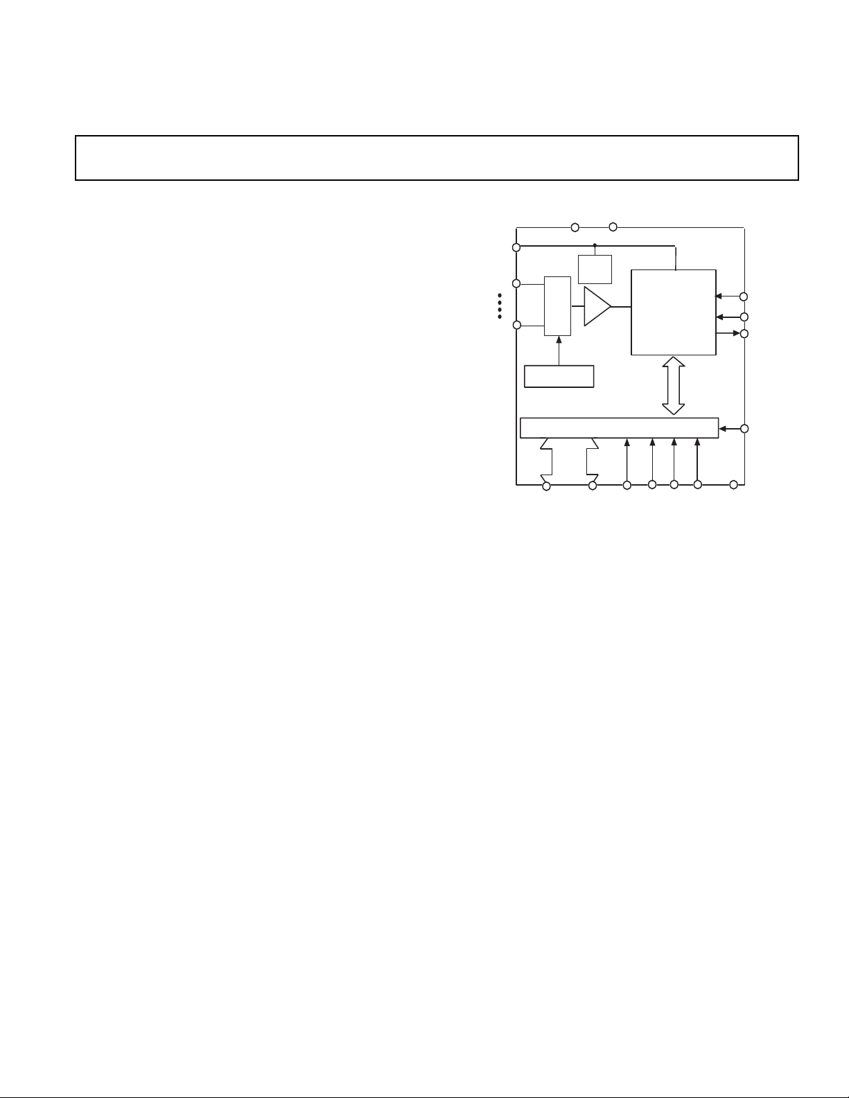
FUNCTIONAL BLOCK DIAGRAM
GENERAL DESCRIPTION
The AD7936/AD7935 are 12- & 10-bit, high speed,
low power, successive approximation (SAR) ADCs.
The parts operate from a single 2.7 V to 5.25 V power
supply and feature throughput rates up to 1.5 MSPS.
The parts contain a low noise, wide bandwidth, differential track/hold amplifier that can handle input
frequencies up to 20MHz.
The AD7936/AD7935 feature 8 analog input channels
with a channel sequencer to allow a pre-programmed
selection of channels to be converted sequentially.
These parts can operate with either Single-ended, Fully
Differential or Pseudo Differential analog inputs. The
analog input configuration is chosen by setting the relevant bits in the on-chip Control Register.
The conversion process and data acquisition are controlled using standard control inputs allowing easy
interfacing to Microprocessors and Dsps. The input
signal is sampled on the falling edge of CONVST and
the conversion is also initiated at this point.
The AD7936/AD7935 has an accurate on-chip 2.5 V
reference that can be used as the reference source for
the analog to digital conversion. Alternatively, this pin
can be overdriven to provide an external reference in
the range 100mV to 3.5 V.
REV.PrA 03/03
Information furnished by Analog Devices is believed to be accurate and
reliable. However, no responsibility is assumed by Analog Devices for its
use, nor for any infringements of patents or other rights of third parties
which may result from its use. No license is granted by implication or
otherwise under any patent or patent rights of Analog Devices.
These parts use advanced design techniques to achieve
very low power dissipation at high throughput rates. They
also feature flexible power management options.
An on-chip Control register allows the user to set up different operating conditions including analog input range
and configuration, output coding, power management and
channel sequencing.
PRODUCT HIGHLIGHTS
1. High Throughput with Low Power Consumption
The AD7936/AD7935 offer 1.5 MSPS throughput
with 8mW power consumption at V
= 3V.
DD
2. Eight Analog Inputs with a Channel Sequencer.
A sequence of input channels can be selected, through
which the AD7936/AD7935 will continuously cycle and
convert on.
3. Accurate on-chip 2.5 V reference.
4. Software Configurable Analog Inputs
Single-Ended, Pseudo Differential or Fully Differential
analog inputs that are software selectable.
5. Single-supply Operation with V
DRIVE
Function.
The AD7936/AD7935 operates from a single 2.7 V to
5.25 V supply. The V
function allows the parallel
DRIVE
interface to connect directly to either 3V or 5 V proces
sor systems independent of V
DD
.
6. No Pipeline Delay
The parts feature a standard successive-approximation
ADC with accurate control of the sampling instant via a
CONVST input and once off conversion control.
One Technology Way, P.O. Box 9106, Norwood, MA 02062-9106,U.S.A.
Tel: 781/329-4700 World Wide Web Site: http://www.analog.com
Fax: 781/326-8703 © Analog Devices, Inc., 2003
Page 2

PRELIMINARY TECHNICAL DATA
AD7936–SPECIFICATIONS
1
( VDD = V
F
CLKIN
=2.7 V to 5.25V, V
DRIVE
= 20MHz, F
= 1.5 MSPS; TA = T
SAMPLE
REFIN/VREFOUT
= 2.5V unless otherwise noted,
to T
MIN
, unless otherwise noted.)
MAX
Parameter BVersion1 Units Test Conditions/Comments
DYNAMIC PERFORMANCE F
Signal to Noise + Distortion
(SINAD)
Signal to Noise Ratio (SNR)
Total Harmonic Distortion (THD)
Peak Harmonic or Spurious Noise -75 dB max -82dB typ
(SFDR)
2
Intermodulation Distortion (IMD)
2
2
2
2
70 dB min
70 dB min
-75 dB max -80dB typ
=50kHz Sine Wave
IN
fa = 40.1kHz, fb = 51.5kHz
Second Order Terms -85 dB typ
Third Order Terms -85 dB typ
Aperture Delay 10 ns typ
Aperture Jitter 50 ps typ
Channel-to-Channel Isolation
2
-8 2 dB typ
Full Power Bandwidth 20 MHz typ @ 3 dB
2.5 MHz typ @ 0.1 dB
DC ACCURACY
Resolution 12 Bits
Integral Nonlinearity
Differential Nonlinearity
Total Unadjusted Error TBD LSB max
0V to V
Input Range
REF IN
2
2
3
±1 LSB max
±0.95 LSB max Guaranteed No Missed Codes to 12 Bits.
Straight Binary Output Coding
Offset Error ±3 LSB max
Offset Error Match ±0.5 LSB max
Gain Error ±2 LSB max
Gain Error Match ±0.6 LSB max
0V to 2 x V
Input Range
REF IN
4
-V
REF IN
to +V
Biased about V
REF IN
REF
with
Twos Complement Output Coding
Positive Gain Error ±2 LSB max
Positive Gain Error Match ±0.6 LSB max
Zero Code Error ±3 LSB max
Zero Code Error Match ±1 LSB max
Negative Gain Error ±1 LSB max
Negative Gain Error Match ±0.5 LSB max
ANALOG INPUT
Input Voltage Ranges 0 to V
REF
0 to 2xV
V RANGE bit in the Control register set to 1.
V RANGE bit in the Control register set to 0.
REF
V
DD/VDRIVE
= 4.75 V to 5.25 V for 0-2V
DC Leakage Current ±1 µA max
Input Capacitance 20 pF typ
REFERENCE INPUT/OUTPUT
V
Input Voltage 2.5
REFIN
5
V ±1% Specified Performance
DC Leakage Current ±1 µA max
V
V
V
Output Voltage 2.49/2.51 Vmin/max
REFOUT
Tempco 15 ppm/°C typ
REFOUT
Output Impedance 10 Ω
REF
LOGIC INPUTS
Input High Voltage, V
Input Low Voltage, V
Input Current, I
IN
Input Capacitance, C
0.7xV
INH
0.3xV
INL
6
IN
DRIVE
DRIVE
V min
V max
± 1 µA max Typically 10 nA, V
10 pF max
= 0 V or V
IN
DRIVE
LOGIC OUTPUTS
Output High Voltage, V
Output Low Voltage, V
Floating-State Leakage Current ±10 µA max
Floating-State Output Capacitance
V
OH
OL
6
-0.2 V min I
DRIVE
0.4 V max I
10 pF max
= 200 µA; VDD = 2.7 V to 5.25 V
SOURCE
=200µA
SINK
Output Coding Straight (Natural) Binary CODING bit in the control register set to 1.
2s Complement CODING bit in the control register set to 0.
REF
range
–2–
REV. PrA
Page 3

PRELIMINARY TECHNICAL DATA
AD7936–SPECIFICATIONS
1
Parameter B Version
1
Units Test Conditions/Comments
CONVERSION RATE
Conversion Time 12 CLKIN
cycles (max)
Track/Hold Acquisition Time 300 ns max Sine Wave Input
325 ns max Full-Scale Step Input
Throughput Rate 1.5 MSPS max Conversion Time + Acquisition Time
POWER REQUIREMENTS
V
DD
V
DRIVE
I
DD
Normal Mode(Static) 0.5 mA typ V
Normal Mode (Operational) 3.2 mA max V
2.7/5.25 V min/max
2.7/5.25 V min/max
2.6 mA max V
Digital I/Ps = 0V or V
= 2.7V to 5.25V.
DD
= 4.75V to 5.25V.
DD
= 2.7V to 3.6V.
DD
DRIVE
.
Auto StandBy Mode 1.55 mA typ
90 µA max (Static)
Auto Shutdown Mode 1 mA typ
1 µA max (Static)
Full Shut-Down Mode 1 µA max SCLK On or Off.
Power Dissipation
Normal Mode (Operational) 16 mW max V
8 mW max V
Auto Standby-Mode (Static) 450 µW max V
270 µW max V
Auto Shutdown-Mode (Static) 5 µW max V
3 µW max V
Full Shutdown-Mode 5 µW max V
= 5V.
DD
= 3V.
DD
= 5V.
DD
= 3V.
DD
= 5V.
DD
= 3V.
DD
= 5V.
DD
3 µW max VDD = 3V.
NOTES
1
Temperature ranges as follows: B Versions: –40°C to +85°C.
2
See Terminology Section.
3
Bit 9 in the Control register set to 1
4
Bit 9 in the Control register set to 0
5
This device is operational with an external reference in the range 0.1 V to 3.5 V.
6
Sample tested @ +25°C to ensure compliance.
Specifications subject to change without notice.
REV. PrA
–3–
Page 4

PRELIMINARY TECHNICAL DATA
AD7935–SPECIFICATIONS
1
( VDD = V
F
CLKIN
=2.7 V to 5.25V, V
DRIVE
= 20MHz, F
= 1.5MSPS; TA = T
SAMPLE
REFIN/VREFOUT
= 2.5V unless otherwise noted,
to T
MIN
, unless otherwise noted.)
MAX
Parameter B Version1 Units Test Conditions/Comments
DYNAMIC PERFORMANCE F
Signal to Noise + Distortion
(SINAD)
Signal to Noise Ratio (SNR)
Total Harmonic Distortion (THD)
Peak Harmonic or Spurious Noise
(SFDR)
Intermodulation Distortion (IMD)
2
2
2
2
60 dB min
60 dB min
-73 dB max
-73 dB max
2
=50kHz Sine Wave
IN
fa = 40.1kHz, fb = 51.5kHz
Second Order Terms -75 dB typ
Third Order Terms -75 dB typ
Aperture Delay 10 ns typ
Aperture Jitter 50 ps typ
Channel-to-Channel Isolation
2
-8 2 dB typ
Full Power Bandwidth 20 MHz typ @ 3 dB
2.5 MHz typ @ 0.1 dB
DC ACCURACY
Resolution 10 Bits
Integral Nonlinearity
2
±0.5 LSB max
Differential Nonlinearity ±0.5 LSB max Guaranteed No Missed Codes to 10 Bits.
Total Unadjusted Error TBD LSB max
0V to V
Input Range
REF IN
3
Straight Binary Output Coding
Offset Error ±3 LSB max
Offset Error Match ±0.5 LSB max
Gain Error ±2 LSB max
Gain Error Match ±0.6 LSB max
0V to 2 x V
Input Range
REF IN
4
-V
REF IN
to +V
Biased about V
REF IN
REF
with
Twos Complement Output CodingOffset
Positive Gain Error ±2 LSB max
Positive Gain Error Match ±0.6 LSB max
Zero Code Error ±3 LSB max
Zero Code Error Match ±1 LSB max
Negative Gain Error ±1 LSB max
Negative Gain Error Match ±0.5 LSB max
ANALOG INPUT
Input Voltage Ranges 0 to V
REF
0 to 2xV
V RANGE bit in the Control register set to 1.
V RANGE bit in the Control register set to 0.
REF
V
DD/VDRIVE
= 4.75 V to 5.25 V for 0-2V
REF
DC Leakage Current ±1 µA max
Input Capacitance 20 pF typ
REFERENCE INPUT/OUTPUT
V
Input Voltage 2.5
REFIN
5
V ±1% Specified Performance
DC Leakage Current ±1 µA max
Input Impedance 36 kΩ
V
REFIN
V
V
V
Output Voltage 2.49/2.51 Vmin/max
REFOUT
Tempco 15 ppm/°C typ
REFOUT
Output Impedance 10 Ω
REF
LOGIC INPUTS
Input High Voltage, V
Input Low Voltage, V
Input Current, I
IN
Input Capacitance, C
0.7xV
INH
0.3xV
INL
6
IN
DRIVE
DRIVE
V min
V max
± 1 µA max Typically 10 nA, V
10 pF max
= 0 V or V
IN
DRIVE
LOGIC OUTPUTS
Output High Voltage, VOH V
Output Low Voltage, V
Floating-State Leakage Current ±10 µA max
Floating-State Output Capacitance
OL
6
-0.2 V min I
DRIVE
0.4 V max I
10 pF max
= 200 µA; VDD = 2.7 V to 5.25 V
SOURCE
=200µA
SINK
Output Coding Straight (Natural) Binary CODING bit in the control register set to 1.
2s Complement CODING bit in the control register set to 0.
–4–
REV. PrA
range
Page 5

PRELIMINARY TECHNICAL DATA
AD7935–SPECIFICATIONS
1
Parameter B Version
1
Units Test Conditions/Comments
CONVERSION RATE
Conversion Time 10 CLKIN
cycles (max)
Track/Hold Acquisition Time 300 ns max Sine Wave Input
325 ns max Full-Scale Step Input
Throughput Rate 1.5 MSPS max Conversion Time + Acquisition Time
POWER REQUIREMENTS
V
DD
V
DRIVE
I
DD
Normal Mode(Static) 0.5 mA typ V
Normal Mode (Operational) 3.2 mA max V
2.7/5.25 V min/max
2.7/5.25 V min/max
2.6 mA max V
Digital I/Ps = 0V or V
= 2.7V to 5.25V.
DD
= 4.75V to 5.25V.
DD
= 2.7V to 3.6V.
DD
DRIVE
.
Auto StandBy Mode 1.55 mA typ
90 µA max (Static)
Auto Shutdown Mode 1 mA typ
1 µA max (Static)
Full Shut-Down Mode 1 µA max SCLK On or Off.
Power Dissipation
Normal Mode (Operational) 16 mW max V
8 mW max V
Auto Standby-Mode (Static) 450 µW max V
270 µW max V
Auto Shutdown-Mode (Static) 5 µW max V
3 µW max V
Full Shutdown-Mode 5 µW max V
= 5V.
DD
= 3V.
DD
= 5V.
DD
= 3V.
DD
= 5V.
DD
= 3V.
DD
= 5V.
DD
3 µW max VDD = 3V.
NOTES
1
Temperature ranges as follows: B Versions: –40°C to +85°C.
2
See Terminology Section
3
Bit 9 in the Control register set to 1
4
Bit 9 in the Control register set to 0
5
This device is operational with an external reference in the range 0.1 V to 3.5 V.
6
Sample tested @ +25°C to ensure compliance.
Specifications subject to change without notice.
REV. PrA
–5–
Page 6

PRELIMINARY TECHNICAL DATA
AD7936/AD7935
( VDD = V
F
CLKIN
TIMING SPECIFICATIONS
Limit at T
MIN
, T
MAX
1,2, 3
Parameter AD7936 AD7935 Units Description
4
f
CLKIN
10 10 kHz min
20 20 MHz max
t
quiet
t
convert
t
1
t
2
t
3
t
4
t
5
t
6
t
7
t
8
t
9
t
10
5
t
11
6
t
12
100 100 ns min Minimum time between conversions
TBD TBD ns max Conversion Time
100 100 ns min CONVST pulsewidth
0 0 ns min CS to WR setup time
0 0 ns max CS to WR hold time
55 5 5 ns min WR Pulse Width
10 1 0 ns min Data Setup time before WR
5
1/2 t
CLKIN
5 ns min Data Hold after WR
1/2 t
CLKIN
ns min New data valid before falling edge of BUSY
0 0 ns min CS to RD setup time
0 0 ns max CS to RD hold time
55
50
55 ns min RD Pulse Width
50 ns max Data access time after RD
5 5 ns min Bus relinquish time after RD
40 40 ns max Bus relinquish time after RD
t
13
t
14
t
15
t
16
t
17
15 1 5 ns min HBEN to RD setup time
5 5 ns min HBEN to RD hold time
60 60 ns min/max Minimum time between Reads
0 0 ns min HBEN to WR setup time
5 5 ns max HBEN to RD setup time
=2.7 V to 5.25V, V
DRIVE
= 20MHz, F
= 1.5MSPS; TA = T
SAMPLE
REFIN/VREFOUT
= 2.5V unless otherwise noted,
to T
MIN
, unless otherwise noted.)
MAX
NOTES
1
Sample tested at +25°C to ensure compliance. All input signals are specified with tr = tf = 5 ns (10% to 90% of V
level of 1.6 Volts.
2
See Figure 20 and 21.
3
All timing specifications given above are with a 25pF load capacitance.
4
Mark/Space ratio for the SCLK input is 40/60 to 60/40.
5
The time required for the output to cross 0.4 V or 0.7 x V
6
t12 is derived form the measured time taken by the data outputs to change 0.5 V. The measured number is then extrapolated back to remove
the effects of charging or discharging the 25 pF capacitor. This means that the time, t12 quoted in the timing characteristics is the true bus
relinquish time of the part and is independent of the bus loading.
Specifications subject to change without notice.
DRIVE
V.
) and timed from a voltage
DD
–6–
REV. PrA
Page 7

PRELIMINARY TECHNICAL DATA
AD7936/AD7935
ABSOLUTE MAXIMUM RATINGS
(TA = +25°C unless otherwise noted)
1
VDD to AGND/DGND . . . . . . . . . . . . . . . . . –0.3 V to 7 V
to AGND/DGND . . . . . . . . . . . . . . . –0.3 V to 7 V
V
DRIVE
Analog Input Voltage to AGND . –0.3 V to V
+ 0.3 V
DD
Digital Input Voltage to DGND . . . . . . . . . . –0.3 V to 7 V
to V
V
DRIVE
Digital Output Voltage to AGND –0.3 V to V
REF
to AGND . . . . . . . . . ........–0.3 V to VDD + 0.3 V
IN
Input Current to Any Pin Except Supplies
. . . . . . . . . . . . . . . . . . . . . . . . .
DD
–0.3 V to VDD + 0.3 V
+ 0.3 V
DD
2
. . . . ±10 mA
Operating Temperature Range
Commercial (B Version) . . . . . . . . . . . –40°C to +85°C
Storage Temperature Range . . . . . . . –65°C to +150°C
Junction Temperature . . . . . . . . . . . . . . . . . . . . . . . +150°C
Thermal Impedance . . . . . . . . . . . . . 97.9°C/W (TSSOP
θ
JA
Thermal Impedance . . . . . . . . . . . . . . 14°C/W (TSSOP)
θ
JC
Lead Temperature, Soldering
Vapor Phase (60 secs) . . . . . . . . . . . . . . . . . . . +215°C
Infared (15 secs) . . . . . . . . . . . . . . . . . . . . . . . +220°C
E S D . . . . . . . . . . . . . . . . . . . . . . . . . . . . . . . . . . . . . . . . 1 kV
NOTES
1
Stresses above those listed under “Absolute Maximum Ratings” may
cause permanent damage to the device. This is a stress rating only and
functional operation of the device at these or any other conditions above
those listed in the operational sections of this specification is not implied.
Exposure to absolute maximum rating conditions for extended periods
may affect device reliability.
2
Transient currents of up to 100 mA will not cause SCR latch up.
ORDERING GUIDE
Linearity Package Package
Model Range Error (LSB)1 Option Descriptions
AD7936 -40°C to +85°C ±1 RU-28 TSSOP
AD7935 -40°C to +85°C ±1 RU-28 TSSOP
EVAL-ADxxxxCB
EVAL-CONTROL BRD2
NOTES
1
Linearity error here refers to integral linearity error.
2
This can be used as a stand-alone evaluation board or in conjunction with the Evaluation Board Controller for evaluation/demonstration purposes.
3
Evaluation Board Controller. This board is a complete unit allowing a PC to control and communicate with all Analog Devices evaluation boards
ending in the CB designators. The following needs to be ordered to obtain a complete evaluation kit: the ADC Evaluation Board (EVALADxxxxCB), the EVAL-CONTROL BRD2 and a 12 V ac transformer. See the ADxxxx evaluation board technical note for more details.
2
3
Evaluation Board
Controller Board
CAUTION
ESD (electrostatic discharge) sensitive device. Electrostatic charges as high as 4000 V readily
accumulate on the human body and test equipment and can discharge without detection. Although
the AD7936/AD7935 features proprietary ESD protection circuitry, permanent
damage may occur on devices subjected to high-energy electrostatic discharges.
Therefore, proper ESD precautions are recommended to avoid performance degradation
or loss of functionality.
REV. PrA
–7–
Page 8

AD7936/AD7935
PRELIMINARY TECHNICAL DATA
PIN CONFIGURATION TSSOP
VIN7
V
HBEN
DB0
DB1
DB3
DB4
DB5
DB6
DB7
V
DRIVE
DGND
BUSY
CLKIN
DD
DB2
1
AD7936/
2
AD7935
3
4
5
TOP VIEW
6
(Not to
Scale)
7
8
9
10
11
12
13
28
VIN6
27
VIN5
26
VIN4
25
VIN3
24
VIN2
23
VIN1
22
VIN0
21
V
20
REFIN/REFOUT
19
AGND
CS
18
RD
17
WR
16
CONVST
1514
PIN FUNCTION DESCRIPTION
Pin no. Pin Mnemonic Function
1 V
DD
Power Supply Input. The VDD range for the AD7936/AD7935 is from +2.7V to +5.25V.
The supply should be decoupled to AGND with a 0.1µF capacitor and a 10µF tantalum
capacitor.
2 HBEN High Byte Enable. When HBEN is low, the low byte of data being written to or read from
the AD7936/AD7935 is on DB0 to DB7. When reading from the AD7935, the two LSBs in
the low byte are zeros, followed by 6 bits of conversion data. When HBEN is high, the top 4
bits of the data being written to or read from the AD7936/AD7935 are on DB0 to DB3.
When reading from the device, DB4 & DB5 of the high byte will contain the ID of the
channel for which the conversion result corresponds.
3-10 DB0 to DB7 Data Bits 0 to 7. Three state parallel digital I/O pins that provide the conversion result and
also allow the Control and Shadow registers to be programmed. These pins are controlled by
CS, RD and WR. The state of the HBEN input determines which byte of data is written to
or read from the bus.The logic high voltage level for these pins is determined by the V
DRIVE
input.
11 V
DRIVE
Logic Power Supply Input. The voltage supplied at this pin determines at what voltage the
parallel interface of the AD7936/AD7935 will operate.
12 DGND Digital Ground. This is the ground reference point for all digital circuitry on the AD7936/
AD7935. The DGND and AGND voltages should ideally be at the same potential and must
not be more than 0.3 V apart, even on a transient basis.
13 BUSY Busy Output. Logic output indicating the status of the conversion. The BUSY output goes
high following the falling edge of CONVST and stays high for the duration of the
conversion. Once the conversion is complete and the result is available in the output register,
the BUSY output will go low. The track/hold returns to track mode just prior to the falling
edge of BUSY and the acquisition time for the part begins when BUSY goes low.
14 CLKIN Master Clock Input. The clock source for the conversion process is applied to this pin.
Conversion time for the AD7936 takes 12 clock cycles while conversion time for the AD7935
takes 10 clock cycles. The frequency of the master clock input therefore determines the
conversion time and achievable throughput rate.
–8–
REV. PrA
Page 9

PRELIMINARY TECHNICAL DATA
AD7936/AD7935
PIN FUNCTION DESCRIPTION
Pin no. Pin Mnemonic Function
15 CONVST Conversion Start Input. Following power down, when operating in Auto-shutdown or Auto
STBY modes, a rising edge on CONVST is used to power up the device. A falling edge on
CONVST is used to initiate a conversion. The track/hold goes from track to hold mode on
the falling edge of CONVST and the conversion process is initiated at this point.
16 WR Write Input. Active low logic input used in conjunction with CS to write data to the internal
registers.
17 RD Read Input. Active low logic input used in conjunction with CS to access the conversion
result. The conversion result is placed on the data bus following the falling edge of both CS
and RD.
18 CS Chip Select. Active low logic input used in conjunction with RD , WR and HBEN to Read
conversion data or to Write data to the internal registers. When reading, depending on the
state of the HBEN input, the low or high byte of data is placed on to the data bus following
the falling edge of both CS and RD.
19 AGND Analog Ground. This is the ground reference point for all analog circuitry on the AD7936/
AD7935. All analog input signals and any external reference signal should be referred to this
AGND voltage. The AGND and DGND voltages should ideally be at the same potential and
must not be more than 0.3 V apart, even on a transient basis.
20 V
21-28 V
REFIN/VREFOUT
0 - VIN7 Analog Input 0 to Analog Input 7. Eight analog input channels that are multiplexed into the
IN
Reference Input/Output. This pin is connected to the internal reference and is the reference
source for the ADC. The nominal internal reference voltage is 2.5 V and this appears at this
pin. This pin can be overdriven by an external reference. The input voltage range for the
external reference is 0.1 V to 3.5 V.
on-chip track/hold. The analog inputs can be programmed to be eight single ended inputs,
four fully differential pairs, four pseudo differential pairs or 7 pseudo differential inputs by
setting the MODE bits in the Control register appropriately (see Table III). The analog
input channel to be converted can either be selected by writing to the Address bits (ADD2,
ADD1 & ADD0) in the control register prior to the conversion, or the on-chip sequencer can
be used. The address bits in conjunction with the SEQ and SHDW bits in the Control register
allow the Sequencer and Shadow register to be programmed. The input range for all input
channels can either be 0V to V
complement, depending on the states of the RANGE and CODING bits in the Control
register. Any unsed input channels should be connected to AGND to avoid noise pickup.
or 0V to 2 x V
REF
and the coding can be binary or two’s
REF
REV. PrA
–9–
Page 10

AD7936/AD7935
PRELIMINARY TECHNICAL DATA
TERMINOLOGY
Integral Nonlinearity
This is the maximum deviation from a straight line passing through the endpoints of the ADC transfer function.
The endpoints of the transfer function are zero scale, a
point 1 LSB below the first code transition, and full scale,
a point 1 LSB above the last code transition.
Differential Nonlinearity
This is the difference between the measured and the ideal 1
LSB change between any two adjacent codes in the ADC.
Offset Error
This is the deviation of the first code transition (00 . . .
000) to (00 . . . 001) from the ideal, i.e AGND + 1 LSB
Offset Error Match
This is the difference in offset error between any two channels.
Gain Error
This is the deviation of the last code transition (111 . . .
110) to (111 . . . 111) from the ideal (i.e., V
REFIN
– 1
LSB) after the offset error has been adjusted out.
Gain Error Match
This is the difference in Gain error between any two channels.
Zero Code Error
This applies when using the 2’s complement output coding option, in particular to the 2 x V
-V
REFIN
to +V
biased about the V
REFIN
input range with
REFIN
REFIN
point. It is
the deviation of the mid scale transition (all 0s to all 1s)
from the ideal V
voltage, i.e. V
IN
REFIN
- 1 LSB.
Zero Code Error Match
This is the difference in Zero Code Error between any two
channels.
Positive Gain Error
This applies when using the 2’s complement output coding option, in particular to the 2 x V
-V
REFIN
to +V
biased about the V
REFIN
input range with
REFIN
point. It is the
REFIN
deviation of the last code transition (011. . .110) to (011 .
. . 111) from the ideal (i.e., +V
- 1 LSB) after the
REFIN
Zero Code Error has been adjusted out.
Positive Gain Error Match
This is the difference in Positive Gain Error between any
two channels.
Negative Gain Error
This applies when using the 2’s complement output coding option, in particular to the 2 x V
-V
REFIN
to +V
biased about the V
REFIN
input range with
REFIN
point. It is the
REFIN
deviation of the first code transition (100 . . . 000) to (100
. . . 001) from the ideal (i.e., -REF
+ 1 LSB) after the
IN
Zero Code Error has been adjusted out.
Negative Gain Error Match
This is the difference in Negative Gain Error between any
two channels.
Channel-to-Channel Isolation
Channel-to-Channel Isolation is a measure of the level of
crosstalk between channels. It is measured by applying a
fullscale 390 kHz sine wave signal to all 7 nonselected
input channels and determining how much that signal is
attenuated in the selected channel with a 50 kHz signal.
The figure is given worse case across all 8 channels for the
AD7936/AD7935.
PSR (Power Supply Rejection)
Varations in power supply will affect the full scale transi-
–10–
tion, but not the converter’s linearity. Power supply rejection is the maximum change in full-scale transition point
due to a change in power-supply voltage from the nominal
value. See Typical PerformancePlots.
Track/Hold Acquisition Time
The track/hold amplifier returns into track mode and the
end of conversion. Track/Hold acquisition time is the time
required for the output of the track/hold amplifier to reach
its final value, within ±1/2 LSB, after the end of conversion.
Signal to (Noise + Distortion) Ratio
This is the measured ratio of signal to (noise + distortion)
at the output of the A/D converter. The signal is the rms
amplitude of the fundamental. Noise is the sum of all
nonfundamental signals up to half the sampling frequency
/2), excluding dc. The ratio is dependent on the number
(f
S
of quantization levels in the digitization process; the more
levels, the smaller the quantization noise. The theoretical
signal to (noise + distortion) ratio for an ideal N-bit converter with a sine wave input is given by:
Signal to (Noise + Distortion) = (6.02 N + 1.76) dB
Thus for a 12-bit converter, this is 74 dB and for a 10-bit
converter, this is 61.96dB.
Total Harmonic Distortion
Total harmonic distortion (THD) is the ratio of the rms
sum of harmonics to the fundamental. For the AD7936/
AD7935, it is defined as:
2
2
2
2
2
+ V
5
6
THD (dB ) = 20 log
+ V
+ V
V
2
3
+ V
4
V
1
where V1 is the rms amplitude of the fundamental and V2,
V
, V4, V5 and V6 are the rms amplitudes of the second
3
through the sixth harmonics.
Peak Harmonic or Spurious Noise
Peak harmonic or spurious noise is defined as the ratio of
the rms value of the next largest component in the ADC
output spectrum (up to f
/2 and excluding dc) to the rms
S
value of the fundamental. Normally, the value of this specification is determined by the largest harmonic in the
spectrum, but for ADCs where the harmonics are buried in
the noise floor, it will be a noise peak
Intermodulation Distortion
With inputs consisting of sine waves at two frequencies, fa
and fb, any active device with nonlinearities will create
distortion products at sum and difference frequencies of mfa
± nfb where m, n = 0, 1, 2, 3, etc. Intermodulation distortion terms are those for which neither m nor n are equal to
zero. For example, the second order terms include (fa + fb)
and (fa – fb), while the third order terms include (2fa + fb),
(2fa – fb), (fa + 2fb) and (fa – 2fb).
The AD7936/AD7935 is tested using the CCIF standard
where two input frequencies near the top end of the input
bandwidth are used. In this case, the second order terms are
usually distanced in frequency from the original sine waves
while the third order terms are usually at a frequency close
to the input frequencies. As a result, the second and third
order terms are specified separately. The calculation of the
intermodulation distortion is as per the THD specification
where it is the ratio of the rms sum of the individual distortion products to the rms amplitude of the sum of the
fundamentals expressed in dBs.
REV. PrA
Page 11

0
TITLE
0
0
0
000
T
I
T
L
E
0000
6*,
E
L
T
0
I
T
6*,
0
000
0000
TITLE
TPC1 PSRR versus Supply ripple
Frequencywith supply decoupling
0
E
L
T
0
I
T
6*,
PRELIMINARY TECHNICAL DATA
TYPICAL PERFORMANCE CHARACTERISTICS
AD7936 Performance Curves
0
E
L
T
I
T
E
L
T
0
I
T
0
000
TPC5. AD7936 SINAD vs Analog Input
Frequency for various Supply Volt-
0
6*,
0000
TITLE
ages
TPC9. Change in INL vs V
0
E
L
T
0
I
T
AD7936/AD7935
0
0
0
000
6*,
0000
TITLE
V
= 5V
DD
6*,
REF
for
0
000
0000
TITLE
TPC2 PSRR versus Supply ripple
Frequencywithout supply decoupling
0
E
L
T
0
I
T
0
000
TPC3 Internal V
6*,
0000
TITLE
Error vs
REF
Temperature
0
E
L
T
0
I
T
0
000
6*,
0000
TITLE
TPC6. FFT @ VDD = 5V
0
E
L
T
0
I
T
0
000
6*,
0000
TITLE
TPC7. Typical DNL @ VDD = 5V
0
0
000
0000
TITLE
TPC10. Change in DNL vs V
VDD = 5V
0
E
L
T
0
I
T
0
000
6*,
0000
TITLE
TPC11. Change in ENOB vs V
VDD = 5V
REF
REF
for
for
E
L
T
0
I
T
0
000
TPC4 V
0000
REF
REV. PrA
6*,
TITLE
out vs Rsource
E
L
T
0
I
T
0
000
6*,
0000
TITLE
TPC8. Typical INL @ VDD = 5V
–11–
TPC12. Offset vs V
REF
Page 12

AD7936/AD7935
PRELIMINARY TECHNICAL DATA
E
L
T
I
T
0
0
0
000
6*,
0000
TITLE
AD7935 Performance Curves
0
E
L
T
0
I
T
6*,
0
000
0000
TITLE
E
L
T
I
T
0
0
0
000
6*,
0000
TITLE
0
E
L
T
0
I
T
0
000
6*,
0000
TITLE
TPC13. Histogram of codes TPC13. FFT @ VDD = 5V TPC 14. Typical DNL TPC 15. Typcial INL
@ VDD = 5v @ V
= 5V @ VDD = 5V
DD
ON-CHIP REGISTERS
The AD7936/AD7935 has two on-chip registers that are necessary for the operation of the device. These are the Control
register, used to set up different conditions and the Shadow register, used to program the analog input channels to be
converted on.
CONTROL REGISTER
The Control Register on the AD7936/AD7935 is a 12-bit, write-only register. Data is written to this register using the
CS and WR pins. The Control Register is shown below and the functions of the bits are described in Table I.
MSB
D11
D1D2D3D4D6D7D8D9D10 D5
PM1 PM0 CODING REF ADD2 ADD1 ADD0 MODE1 MODE0 SHDW SEQ RANGE
LSB
D0
Table I. Control Register Bit Function Description
Bit Mnemonic Comment
11, 10 PM1 Power Management Bits. These two bits are used to select the power mode of operation. The
PM0 user can choose between either normal mode or various power down modes of operation as shown
in Table II.
9 C O DI N G This bit selects the output coding of the conversion result. If this bit is set to 0, the output
coding will be 2s complement. If this bit is set to 1, the output coding will be straight binary.
8 R E F This bit selects whether the internal or an external reference is used to perform the conversion. If
this bit is logic 0, the internal reference is selected and if it is 1, an external reference should be
applied (see the Reference Section).
7, 6, 5 ADD2, These three address bits are used to either select which analog input channel is to be converted on
ADD1, in the next conversion if the sequencer is not being used, or to select the final channel in a
ADD0 consecutive sequence when the sequencer is being used as described in Table IV. The selected
input channel is decoded as shown in Table III.
4,3 MODE1, The two Mode pins select the type of analog input on the eight V
pins. The AD7936/AD7935
IN
MODE0 can have either 8 Single Ended inputs, 4 Fully Differential inputs, 4 Pseudo Differential inputs or
7 Pseudo Differential inputs. See Table III.
2 SHDW The SHDW bit in the control register is used in conjunction with the SEQ bit to control the
sequencer function and access the SHADOW register. See Table IV.
1 S E Q The SEQ bit in the control register is used in conjunction with the SHDW bit to control the
sequencer function and access the SHADOW register. See Table IV.
0 RANGE This bit selects the analog input range of the AD7936/AD7935. If it is set to 0 then the analog
input range will extend from 0V to V
extend from 0V to 2xV
. When this range is selected, AVDD must be 4.75 V to 5.25 V.
REF
. If it is set to 1 then the analog input range will
REF
–12–
REV. PrA
Page 13

PRELIMINARY TECHNICAL DATA
AD7936/AD7935
Table II. Power Mode Selection using the Power Management Bits in the Control Register
PM1 PM2 Mode Description
1 1 Normal Mode When operating in normal mode, all circuitry is fully powerered up at all times.
1 0 Full Shutdown When the AD7936/AD7935 enters this mode, all circuitry is powered down. The
information in the Control Register is retained.
0 1 Auto Shutdown When operating in Auto Shutdown mode, the AD7936/AD7935 will enter Full Shutdown
mode at the end of each conversion. In this mode, all circuitry is powered down.
0 0 Auto Standby When the AD7936/AD7935 enter this mode, all circuitry is powered down excluding the
internal reference. This mode is similar to Auto Shutdown and allows the part to power up
in 1µsec.
Table III. Analog Input Type Selection
Channel Address MODE0=0, MODE1=0 MODE0=0, MODE1=1 MODE0=1, MODE1=0 MODE0=1, MODE1=1
8 Single-Ended I/P 4 Fully Differential 4 Pseudo Differential 7 Pseudo Differential
Channels I/P Channels I/P Channels I/P Channels
ADD2 ADD1 ADD0 V
0 0 0 VIN0 AGND VIN0 VIN1 VIN0 VIN1 VIN0 VIN7
0 0 1 VIN1 AGND VIN1 VIN0 VIN1 VIN0 VIN1 VIN7
0 1 0 VIN2 AGND VIN2 VIN3 VIN2 VIN3 VIN2 VIN7
0 1 1 VIN3 AGND VIN3 VIN2 VIN3 VIN2 VIN3 VIN7
1 0 0 VIN4 AGND VIN4 VIN5 VIN4 VIN5 VIN4 VIN7
1 0 1 VIN5 AGND VIN5 VIN4 VIN5 VIN4 VIN5 VIN7
1 1 0 VIN6 AGND VIN6 VIN7 VIN6 VIN7 VIN6 VIN7
1 1 1 VIN7 AGND VIN7 VIN6 VIN7 VIN6 VIN7 VIN7
V
IN+
IN-
V
V
IN+
IN-
V
V
IN+
IN-
V
V
IN+
IN-
SEQUENCER OPERATION
The configuration of the SEQ and SHDW bits in the control register allows the user to select a particular mode of operation of
the sequencer function. Table IV outlines the four modes of operation of the Sequencer.
Table IV. Sequence Selection
SEQ SHDW Sequence Type
0 0 This configuration is selected when the sequence function is not used. The analog input channel selected on
each individual conversion is determined by the contents of the channel address bits ADD2-ADD0 in each prior
write operation. This mode of operation reflects the normal operation of a multi-channel ADC, without the
Sequencer function being used, where each write to the AD7936/35 selects the next channel for conversion.
0 1 This configuration selects the Shadow register for programming. The following two write operations will load
the data to the Shadow Register. This will program the sequence of channels to be converted on continuously
after each CONVST falling edge (see the Shadow register description and Table V).
1 0 If the SEQ and SHADOW bits are set in this way then the sequence function will not be interrupted upon
completion of the WRITE operation. This allows other bits in the Control Register to be altered between
conversions while in a sequence without terminating the cycle.
1 1 This configuration is used in conjunction with the Channel Address bits (ADD2 -ADD0) to program
continuous conversions on a consecutive sequence of channels from Channel 0 through to a selected final
channel as determined by the Channel Address bits in the Control Register.
SHADOW REGISTER
The Shadow Register on the AD7936/AD7935 is an 8-bit, write-only register. Data is loaded from DB0 to DB11 on the rising edge of WR. The 8 LSBs will be loaded into the Shadow register. The information is written into the Shadow Register
provided the SEQ and SHADOW bits in the control register were set to 0 & 1 respectively in the previous write to the Control Register. Each bit represents an analog input from channel 0 through to channel 7. A sequence of channels may be
selected through which the AD7936/AD7935 will cycle with each consecutive conversion after the write to the Shadow register. To select a sequence of channels, the associated channel bit must be set for each analog input. The AD7936/AD7935 will
continuously cycle through the selected channels in ascending order, beginning with the lowest channel, until a write operation
occurs with the SEQ and SHADOW bits configured in any way except 1,0 (see Table IV). The bit functions are outlined in
Table V.
REV. PrA
VIN0
Table V. Shadow Register Bit Functions
VIN7VIN6VIN5VIN4VIN3VIN2VIN1
–13–
Page 14

AD7936/AD7935
PRELIMINARY TECHNICAL DATA
CIRCUIT INFORMATION
The AD7936/AD7935 are fast, 8 channel, 12-&10-bit,
single supply, Analog to Digital converters. The parts can
be operated from a either a 2.7 V to 3.6 V or a 4.75 V to
5.25 V power supply and feature throughput rates up to
1.5MSPS.
The AD7936/AD7935 provide the user with an on-chip
track/hold, an internal accurate reference, an analog to
digital converter, and a byte parallel interface housed in a
28-lead TSSOP.
The AD7936/AD7935 have eight analog input channels
which can be configured to be 8 single ended inputs, 4
fully differential pairs, 4 pseudo differential pairs or 7
pseudo differential inputs. There is an on-chip user-programmable channel sequencer which allows the user to
select a sequence of channels through which the ADC can
cycle.
The analog input range for the AD7936/AD7935 is 0 to
V
or 0 to 2 x V
REF
RANGE bit in the Control register. For the 0 to 2 x V
depending on the status of the
REF
REF
range the part must be operated from a 4.75 V to 5.25 V
supply.
The AD7936/AD7935 provides flexible power management options to allow the user to achieve the best power
performance for a given throughput rate. These options
are selected by programming the power management bits,
PM1 and PM0, in the Control Register.
CONVERTER OPERATION
The AD7936/AD7935 is a successive approximation ADC
based around two capacitive DACs. Figures 1 and 2 show
simplified schematics of the ADC in Acquisition and Conversion phase respectively. The ADC comprises of
Control Logic, a SAR and two capacitive DACs. Figure
1 shows the operation of the ADC in Differential/Pseudo
Differential Mode. Single Ended mode operation is similar but V
is internally tied to AGND. In acquisition
IN-
phase, SW3 is closed and SW1 and SW2 are in position
A, the comparator is held in a balanced condition and the
sampling capacitor arrays acquire the differential signal on
the input.
CAPACITIVE
DAC
SW3
COMPARATOR
CONTROL
LOGIC
CAPACITIVE
DAC
C
REF
s
C
s
V
IN+
V
IN-
B
A
SW1
SW2
A
B
V
disconnected once the conversion begins. The Control
Logic and the charge redistribution DACs are used to add
and subtract fixed amounts of charge from the sampling
capacitor arrays to bring the comparator back into a balanced condition. When the comparator is rebalanced, the
conversion is complete. The Control Logic generates the
ADC’s output code. The output impedances of the
sources driving the V
and the V
IN+
pins must be
IN-
matched otherwise the two inputs will have different settling times, resulting in errors.
CAPACITIVE
DAC
SW3
COMPARATOR
CONTROL
LOGIC
CAPACITIVE
DAC
C
REF
s
C
s
V
IN+
V
IN-
B
A
SW1
SW2
A
B
V
Figure 2. ADC Conversion Phase
ADC TRANSFER FUNCTION
The output coding for the AD7936/AD7935 is either
straight binary or two’s complement, depending on the
status of the CODING bit in the control register. The
designed code transitions occur at successive LSB values
(i.e. 1LSB, 2LSBs, etc.) and the LSB size is V
for the AD7936 and V
/1024 for the AD7935. The ideal
REF
REF
/4096
transfer characteristics of the AD7936/AD7935 for both
straight binary and twos complement output coding are
shown in Figures 3 and 4 respectively.
111...111
111...110
111...000
011...111
ADC CODE
000...010
000...001
000...000
0V
NOTE: V
1LSB
1LSB = V
1LSB = V
ANALOG INPUT
is either V
REF
/4096 (AD7936)
REF
/1024 (AD7935)
REF
+V
REF
or 2 X V
REF
-1LSB
REF
Figure 3. AD7936/AD7935 Ideal Transfer Characteristic
with Straight Binary Output Coding
Figure 1. ADC Acquisition Phase
When the ADC starts a conversion (figure 2), SW3 will
open and SW1 and SW2 will move to position B, causing
the comparator to become unbalanced. Both inputs are
–14–
REV. PrA
Page 15

011...111
011...110
000...001
000...000
111...111
ADC CODE
100...010
100...001
100...000
-V
REF
1LSB = 2xV
1LSB = 2xV
+ 1LSB
ANALOG INPUT
(V
PRELIMINARY TECHNICAL DATA
ANALOG INPUT STRUCTURE
/4096 (AD7936)
REF
/1024 (AD7935)
REF
0LSB
- V
IN+
IN-
+V
- 1LSB
REF
)
Figure 6 shows the equivalent circuit of the analog input
structure of the AD7936/AD7935 in Differential/Pseudo
Differential Mode. In Single Ended mode, V
nally tied to AGND. The four diodes provide ESD
protection for the analog inputs. Care must be taken to
ensure that the analog input signals never exceed the supply rails by more than 300mV. This will cause these
diodes to become forward biased and start conducting into
the substrate. These diodes can conduct up to 10mA
without causing irreversible damage to the part.
The capacitors C1, in figure 6 are typically 4pF and can
primarily be attributed to pin capacitance. The resistors
are lumped components made up of the on-resistance of
the switches. The value of these resistors is typically about
100. The capacitors, C2, are the ADC’s sampling capacitors and have a capacitance of 16pF typically.
AD7936/AD7935
is inter-
IN-
Figure 4. AD7936/AD7935 Ideal Transfer Characteristic
with Twos Complement Output Coding
TYPICAL CONNECTION DIAGRAM
Figure 5 shows a typical connection diagram for the
AD7936/AD7935. The AGND and DGND pins are
connected together at the device for good noise supression.
The V
REFIN/VREFOUT
pin is decoupled to AGND with a
0.47µF capacitor to avoid noise pickup if the internal
reference is used. Alternatively, V
REFIN/VREFOUT
can be
connected to a external reference source. In this case, the
V
REFIN/VREFOUT
pin should be decoupled to AGND with a
0.1µF capacitor. In both cases the analog input range can
either be 0V to V
(Range bit = 1) or 0V to 2 x V
REF
REF
(Range bit = 0). The analog input configuration can be
either 8 Single Ended inputs, 4 Differential Pairs, 4
Pseudo Differential Pairs or 7 Pseudo Differential Inputs
(see Table III). The V
or 5V supply. The voltage applied to the V
pin is connected to either a 3V
DD
DRIVE
input
controls the voltage of the digital interface and here, it is
connected to the same 3V supply of the microprocessor to
allow a 3V logic interface (See the digital inputs section).
+3V/+5V
0.1µF 10µF
SUPPLY
For ac applications, removing high frequency components
from the analog input signal is recommended by the use
of an RC low-pass filter on the relevant analog input pins.
In applications where harmonic distortion and signal to
noise ratio are critical, the analog input should be driven
from a low impedance source. Large source impedances
will significantly affect the ac performance of the ADC.
This may necessitate the use of an input buffer amplifier.
The choice of the opamp will be a function of the particular application.
V
DD
D
V
IN+
C1
V
IN-
C1
D
V
DD
D
D
C2
R1
C2
R1
0 to V
0 to 2 x V
2.5V
VREF
REV. PrA
REF
V
/
REF
V
AD7936/AD7935
DD
VIN0
VIN7
AGND
DGND
REFIN/VREFOUT
0.1µF External Vref
0.47µF Internal Vref
HBEN
CLKIN
CS
RD
WR
BUSY
CONVST
DB0
DB7
V
DRIVE
0.1µF
Figure 5. Typical Connection Diagram
10µF
µC/µP
+3V
SUPPLY
Figure 6. Equivalent Analog Input Circuit.
Conversion Phase - Switches Open
Track Phase - Switches Closed
When no amplifier is used to drive the analog input, the
source impedance should be limited to low values. The
maximum source impedance will depend on the amount
of Total Harmonic Distortion (THD) that can be tolerated. The THD will increase as the source impedance
increases and performance will degrade. Figure 7 shows
a graph of the THD versus analog input signal frequency
for different source impedances for both V
= 5 V and 3
DD
V.
–15–
Page 16

AD7936/AD7935
0
E
L
T
0
I
T
6*,
PRELIMINARY TECHNICAL DATA
connection diagram when operating the ADC in single
ended mode.
+2.5
+1.25V
-1.25
0V
V
V
IN
R
R
3R
R
V
0V
V
AD7936/
0
IN
AD7935*
V
V
IN7
REFOUT
0
000
0000
TITLE
Figure 7.THD vs Analog Input Frequency for Various
Source Impedances
Figure 8 shows a graph of THD versus analog input frequency for various supplies, while sampling at 1.5MHz
with an SCLK of 20 MHz. In this case the source impedance is 10.
0
E
L
T
0
I
T
6*,
*Addition Pins Omitted for Clarity
0.1µF
Figure 9. Single Ended Mode Connection Diagram
Differential Mode
The AD7936/AD7935 can have 4 Differential Input Pairs
by setting the MODE0 and MODE1 bits in the control
register to 0 and 1 respectively.
Differential signals have some benefits over single ended
signals including noise immunity based on the device’s
common mode rejection and improvements in distortion
performance. Figure 10 defines the fully differential analog input of the AD7936/AD7935.
V
COMMON
MODE
VOLTAGE
REF
P-to-P
V
REF
P-to-P
V
IN+
V
IN-
AD7936/
AD7935*
0
000
0000
TITLE
Figure 8.THD vs Analog Input Frequency for various
Supply Voltages
THE ANALOG INPUTS
The AD7936/AD7935 has software selectable analog input configurations. The user can choose either 8 Single
Ended Inputs, 4 Fully Differential Pairs, 4 Pseudo Differential Pairs or 7 Pseudo Differential Inputs. The analog
input configuration is chosen by setting the MODE0/
MODE1 bits in the internal control register (See Table
III).
Single Ended Mode
The AD7936/AD7935 can have 8 single ended analog
input channels by setting the MODE0 and MODE1 bits
in the control register both to 0. In applications where the
signal source has a high impedance, it is recommended to
buffer the analog input before applying it to the ADC.
The internal reference is used to externally bias up a bipolar analog input signal. Figure 9 shows a typical
–16–
*Additional Pins Omitted for Clarity
Figure 10. Differential Input Definition
The amplitude of the differential signal is the difference
between the signals applied to the V
each differential pair (i.e. V
IN+
- V
IN+
). V
IN-
and V
and V
IN+
pins in
IN-
IN-
should be simultaneously driven by two signals each of
amplitude V
of the differential signal is therefore -V
to-peak (i.e. 2 x V
that are 180° out of phase. The amplitude
REF
). This is regardless of the common
REF
to +V
REF
REF
peak-
mode (CM). The common mode is the average of the two
signals, i.e. (V
IN+
+ V
)/2 and is therefore the voltage
IN-
that the two inputs are centered on. This results in the
span of each input being CM ± V
to be set up externally and its range varies with V
the value of V
increases, the common mode range de-
REF
/2. This voltage has
REF
REF
. As
creases. When driving the inputs with an amplfier, the
actual common mode range will be determined by the
amplifier’s output voltage swing.
Figures 11 and 12 show how the common mode range
typically varies with V
for both a 5 V and a 3 V power
REF
REV. PrA
Page 17

PRELIMINARY TECHNICAL DATA
AD7936/AD7935
supply. The common mode must be in this range to guarantee the functionality of the AD7936/AD7935.
When a conversion takes place, the common mode is rejected resulting in a virtually noise free signal of amplitude
-V
to +V
REF
corresponding to he digital codes of 0 to
REF
4095.
0
E
L
T
0
I
T
6*,
0
000
Figure 11. Input Common Mode Range versus V
(VDD = 5V and V
0
E
L
T
0
I
T
0000
TITLE
(max) = 3.5V)
REF
6*,
REF
Differential Amplifier
An ideal method of applying differential drive to the AD7936/
AD7935 is to use a differential amplifier such as the AD8138.
This part can be used as a single ended to differential
amplifier or as a differential to differential amplifier. In both
cases the analog input needs to be bipolar. It also provides
common mode level shifting and buffering of the bipolar
input signal. Figure 13 shows how the AD8138 can be used
as a single ended to differential amplifier. The positive and
negative outputs of the AD8138 are connected to the respective inputs on the ADC via a pair of series resistors to
minimize the effects of switched capacitance on the front end
of the ADC. The RC low pass filter on each analog input is
recommended in ac applications to remove high frequency
components of the analog input. The architecture of the
AD8138 results in outputs that are very highly balanced over
a wide frequency range without requiring tightly matched
external components.
If the analog input source being used has zero impedance then
all four resistors (Rg1, Rg2, Rf1, Rf2) should be the same. If
the source has a 50 impedance and a 50 termination for
example, the value of Rg2 should be increased by 25 to
balance this parallel impedance on the input and thus ensure
that both the positive and negative analog inputs have the
same gain (see figure 13). The outputs of the amplifier are
perfectly matched, balanced differential outputs of identical
amplitude and are exactly 180
o
out of phase.
The AD8138 is specified with 3 V, 5 V and ±5 V power
supplies but the best results are obtained when it is supplied
by ±5 V. A lower cost device that could also be used in this
configuration with slight differences in characteristics to the
AD8138 but with similar performance and operation is the
AD8132.
0
000
Figure 12. Input Common Mode Range versus V
(VDD= 3V and V
0000
TITLE
(max) = 2.2V)
REF
REF
Driving Differential Inputs
Differential operation requires that V
multaneously driven with two equal signals that are 180
and V
IN+
be si-
IN-
o
out of phase. The common mode must be set up externally and has a range which is determined by V
REF
, the
power supply and the particular amplifier used to drive the
analog inputs. Differential modes of operation with either
an ac or dc input, provide the best THD performance
over a wide frequency range. Since not all applications
have a signal preconditioned for differential operation,
there is often a need to perform single ended to differential conversion.
REV. PrA
–17–
TBD
Figure 13. Using the AD8138 as a Single Ended to
Differential Amplifier
Pseudo Differential Mode
The AD7936/AD7935 can have 4 Pseudo Differential
pairs or 7 Pseudo Differential inputs by setting the
MODE0 and MODE1 bits in the control register to 1, 0
and 1, 1 respectively. In the case of the 4 Pseudo differential pairs, V
must have an amplitude of V
is connected to the signal source which
IN+
to make use of the full
REF
dynamic range of the part. A DC input in the range
-100mV to +100mV is applied to the V
pin . The volt-
IN-
age applied to this input provides an offset from ground or
Page 18

AD7936/AD7935
PRELIMINARY TECHNICAL DATA
a pseudo ground for the V
input. In the case of the 7
IN+
Pseudo Differential inputs, the 7 inputs are referred to the
voltage applied to V
. The benefit of pseudo differential
IN7
inputs is that they separate the analog input signal ground
from the ADCs ground allowing DC common mode voltages to be cancelled. Figure 14 shows a connection
diagram for Pseudo Differential Mode.
V
REF
P-to-P
DC INPUT
VOLTAGE
RANGE
±100mV
*ADDITIONAL PINS OMITTED FOR CLARITY
V
V
V
REF
IN+
IN-
0.1µF
AD7936/AD7935*
Figure 14. Pseudo Differential Mode Connection Diagram
ANALOG INPUT SELECTION
As illustrated in Table III, the user can set up their analog
input configuration by setting the values in the MODE0
and MODE1 bits in the Control Register. Assuming the
configuration has been chosen, there are different ways of
selecting the analog input to be converted on depending
on the state of the SEQ and SHDW bits in the Control
register.
Using the Sequencer
Programmable Sequence (SEQ = 0, SHDW = 1 )
The AD7936/AD7935 may be configured to automatically
cycle through a number of selected channels using the onchip programmable sequencer by setting SEQ = 0 and
SHDW = 1 in the Control register. The Analog input
channels to be converted on are selected by programming
the relevent bits in the Shadow Register, see Table V.
Once the shadow register has been programmed with the
required sequence, the next conversion executed will be
on the lowest channel programmed in the SHADOW
register. The next conversion will be on the next highest
channel in the sequence and so on. When the last channel
in the sequence has been converted, the ADC will return
to the first channel selected in the Shadow register
It is not necessary to write to the control register once a
sequencer operation has been initiated. The WRITE input must be kept high to ensure that the Control Register
is not accidently overwritten, or a sequence operation
interrupted. If the control register is written to at any
time during the sequence then it must be ensured that the
SEQ and SHDW bits are set to 1,0 to avoid interrupting
the automatic conversion sequence. This pattern will continue until such time as the AD7936/AD7935 is written to
and the SEQ and SHADOW bits are configured with any
bit combination except 1,0. On completion of the sequence, the AD7936/AD7935 sequencer will return to the
first selected channel in the Shadow register and commence the sequence again. Figure 16 shows a flow chart
of the Programmable Sequence operation
Normal Multichannel Operation (SEQ=SHDW= 0)
Any one of eight analog input channels or 4 pairs of channels may be selected for conversion in any order by setting
the SEQ & SHDW bits in the Control register both to 0.
The channel to be converted on is selected by writing to
the address bits ADD2 - ADD0 in the control register to
program the multiplexer prior to the conversion. This
mode of operation is of a normal multichannel ADC
where each data write selects the next channel for conversion. Figure 15 shows a flow chart of this mode of
operation. The channel configurations are shown in table
III.
TBD
Figure 15. Normal Multichannel Operation Flow Chart
TBD
Figure 16. Programmable Sequence Flow Chart
Consecutive Sequence (SEQ =1, SHDW = 1)
A sequence of consecutive channels can be converted on
beginning with channel 0 and ending with a final channel
selected by writing to the ADD2-ADD0 bits in the Control register. This is done by setting the SEQ and SHDW
bits in the control register both to 1. In this mode, the
sequencer can be used without having to write to the
Shadow register. Once the control register has been written to to set this mode up, the next conversion will be on
Channel 0, then Channel 1 and so on until the channel
selected via the address bits is reached. The cycle will
begin again provided the WR input is tied high or if low,
the SEQ and SHDW bits set to 1, 0; then the ADC will
continue its pre-programmed automatic sequence uninterrupted. Figure 17 shows the flow chart of the Consecutive
Sequence mode.
–18–
REV. PrA
Page 19

PRELIMINARY TECHNICAL DATA
AD7936/AD7935
TBD
Figure 17. Consecutive Sequence Mode Flow Chart
REFERENCE SECTION
The AD7936/AD7935 can operate with either the on chip
reference or an external reference. The internal reference
is selected by setting the REF bit in the interal Control
register to 0. A block diagram of the internal reference
circuitry is shown in Figure 18. The internal reference
circuitry includes an on-chip 2.5 V band gap reference,
and a reference buffer. When using the internal reference
the V
REFIN/VREFOUT
with a 0.47µF capacitor. This internal reference not only
provides the reference for the analog to digital conversion
but can also be used externally in the system. It is recommended that the reference output is buffered using an
external precision opamp before applying it anywhere in
the system.
V
REFIN
V
REFOUT
pin should be decoupled to AGND
BUFFER
ADC
REFERENCE
AD7936/
AD7935
/
Therefore, when operating at V
V
can range from 100mV to a maximum value of
REF
3.5V. When V
= 4.75 V, V
DD
= 5 V, the value of
DD
max = 3.17 V.
REF
Example 2:
VINmax = V
VINmax = V
If V
= 3.6V
DD
+ 0.3
DD
+ V
REF
REF
/2
then VINmax = 3.9 V
Therefore 3xV
V
max = 2.6 V
REF
Therefore, when operating at V
V
can range from 100mV to a maximum value of
REF
2.4V. When V
/2 = 3.6 V
REF
= 2.7 V, V
DD
= 3 V, the value of
DD
max = 2 V.
REF
These examples show that the maximum reference applied to the AD7936/AD7935 is directly dependant on the
value applied to V
DD
.
The performance of the part at different reference values
is shown in TBD to TBD. The value of the reference sets
the analog input span and the common mode voltage
range. Errors in the reference source will result in gain
errors in the AD7936/AD7935 transfer function and will
add to specified full scale errors on the part. When using
an external reference, a capacitor of 0.1µF should be used
to decouple the V
pin to AGND.
REF
Table VI lists examples of suitable voltage references that
could be used that are available from Analog Devices and
Figure 19 shows a typical connection diagram for an external reference.
Figure 18. Internal Reference Circuit Block Diagram
Alternatively, an external reference source in the range of
100mV to 3.5V can be applied to the V
REFIN/VREFOUT
pin
of the AD7936/AD7935. An external reference is selected
by setting the REF bit in the interal Control register to
1.When using an external reference, the V
REFIN/VREFOUT
pin should be decoupled to AGND with a 0.1µF capacitor. With a 5 V power supply, the specified reference is
2.5 V and maximum reference is 3.5V. With a 3 V power
supply, the specified reference is 2.5V and the maximum
reference is 2.6 V. In both cases, the reference is functional from 100mV.
It is important to ensure that, when chosing the reference
value, the maximum analog input range (VINmax) is
never greater than V
+ 0.3V to comply with the maxi-
DD
mum ratings of the device. The following two examples
calculate the maximum V
operating the AD7936/AD7935 at V
input that can be used when
REF
of 5 V and 3 V
DD
respectively.
Example 1:
VINmax = V
VINmax = V
If V
= 5 V
DD
+ 0.3
DD
+ V
REF
REF
/2
then VINmax = 5.3 V
Therefore 3xV
V
max = 3.5 V
REF
/2 = 5.3 V
REF
Table VI Examples of Suitable Voltage References
Reference Output Initial Operating
Voltage Accuracy Current
(% max) (µA)
AD589 1.235 1.2-2.8 50
AD1580 1.225 0.08-0.8 50
REF192 2.5 0.08-0.4 45
REF43 2. 5 0.06-0.1 600
AD780 2.5 0.04-0.2 1000
AD7936/
AD7935*
AD780
8
NC
VDD
0.1µF
10nF
0.1µF
*ADDITIONAL PINS OMITTED FOR CLA RITY
Figure 19. Typical V
OpSel
1
2
3
4
VIN
Te mp
GND
REF
7
2.5 V
6
Vout
Tr im
5
Connection Diagram
NC
NC
NC
V
REF
0.1µF
REV. PrA
–19–
Page 20

AD7936/AD7935
PRELIMINARY TECHNICAL DATA
Digital Inputs
The digital inputs applied to the AD7936/AD7935 are not
limited by the maximum ratings which limit the analog
inputs. Instead, the digital inputs applied can go to 7V and
are not restricted by the AV
+0.3V limit as on the ana-
DD
log inputs.
Another advantage of the digital inputs not being re-
stricted by the AV
+ 0.3 V limit is the fact that power
DD
supply sequencing issues are avoided. If any of these inputs are applied before AV
then there is no risk of
DD
latch-up as there would be on the analog inputs if a signal
greater than 0.3 V was applied prior to AV
V
DRIVE
The AD7936/AD7935 has a V
Input
feature. V
DRIVE
DD
.
DRIVE
con-
trols the voltage at which the Parallel Interface operates.
allows the ADC to easily interface to both 3 V and
V
DRIVE
5 V processors. For example, if the AD7936/AD7935
were operated with an AV
of 5V, and the V
DD
DRIVE
pin
could be powered from a 3V supply. The AD7936/
AD7935 has better dynamic performance with an AV
DD
of
5V while still being able to interface to 3V processors.
Care should be taken to ensure V
AV
by more than 0.3 V. (See Absolute Maximum Rat-
DD
does not exceed
DRIVE
ings Section).
PARALLEL INTERFACE
The AD7936/AD7935 has a flexible, high speed, parallel
interface. This interface is 8-bits wide and operates in
Byte mode. The CONVST signal is used to power up the
ADC and to initiate conversions.
A falling edge on the CONVST signal is used to initiate
conversions. Once the CONVST signal goes low, the
BUSY signal goes high for the duration of the Conversion. At the end of the Conversion, BUSY goes low and
can be used to activate an Interrupt Service Routine. The
CS and RD lines are then activated in parallel to read the
high byte and low byte containing the conversion data
depending on the state of the HBEN input. When operating the device Auto Shutdown or Auto Standby mode,
where the ADC powers down at the end of each conversion, a rising edge on the CONVST signal is used to
power up the device.
CONVST
t
1
Reading Data from the AD7936/AD7935
AD7936/AD7935 interface operates in Byte mode. The
12- or 10-bits of conversion data from the AD7936/
AD7935 must be acessed in two read operations with 8
bits of data provided on DB0 to DB7 for each of the read
operations. The HBEN pin determines whether the read
operation accesses the high byte or the low byte of the 12or 10-bit word. For a low byte read, for 12-bit operation,
DB0 to DB7 provide the 8 LSBs of the 12-bit word. For
10-bit operation, the two LSBs of the low byte are zeros
and are followed by 6-bits of conversion data. For a high
byte read, DB0 to DB4 provide the 4MSBs of the 12-/10bit word. The remainder of the bits in the high byte
provide the Channel ID. Figure 20 shows the timing of
the two read cycles shown which are required to access the
conversion data from the device. The CS and RD signals
are gated internally and level triggered active low. CS
and RD may be tied together as the timing specification t
8
and t9 is 0ns min. The data is placed onto the data bus a
time t
after both CS and RD go low. The RD rising
11
edge can be used to latch data out of the device. After a
time, t
, the data lines will become 3 stated.
9
Writing Data to the AD7936/AD7935
The AD7936/AD7935 interface operates in Byte mode
therefore two write operations are required to transfer a
full 12-/10-Bit word into the device. Data to be written
to the AD7936/AD7935 should be provided on the DB0
to DB7 inputs. HBEN determines whether the byte to be
written is high byte or low byte data. For a low byte
write, HBEN should be low and DB0 will contain the
LSB of the data. For the high byte write, HBEN should
be high and the data on the DB0 input should be data bit
8 of the 12-/10-bit word.
Figure 21 shows the timing of the two write cycles shown
which are required to access the full conversion data word
from the device. In figure 21, the first write transfers the
lower 8 bits of data from DB0 to DB7 and the second
write transfers the upper 2 or 4 bits of the data word.
The CS and WR signals are gated internally. CS and
WR may be tied together as the timing specification for t
2
and t3 is 0ns min. The data is latched into the device on
BUSY
HBEN
CS
RD
DB0-DB7
INTERNAL
DATA
LATCH
t
7
OLD DATA
t
13
t
8
t
10
t
11
LOW BYTE
t
9
NEW DATA
t
14
t
12
t
13
t
15
Figure 20. Read Cycle Timing for Byte Mode Operation
–20–
HIGH BYTE
t
14
REV. PrA
Page 21

PRELIMINARY TECHNICAL DATA
AD7936/AD7935
the rising edge of WR. The data needs to be setup a time
before the WR rising edge and held for a time t6 after
t
5
the WR rising edge.
HBEN
CS
WR
DB0-DB7
t
16
t
2
LOW BYTE
t
17
t
3
t
4
t
5
t
6
t
16
HIGH BYTE
t
17
Figure 21. Write Cycle Timing for Byte Mode Operation
MODES OF OPERATION
The AD7936/AD7935 has a number of different power
modes of operation. These modes are designed to provide
flexible power management options. Different options
can be chosen to optimize the power dissipation/throughput rate ratio for differing applications. The mode of
operation is selected by the power management bits, PM1
and PM0, in the Control register, as detailed in Table II.
At power on reset, the default power up condition is normal mode.
Normal Mode (PM1 = PM0 = 1)
This mode is intended for the fastest throughput rate performance as the user does not have to worry about any
power up times as the AD7936/AD7935 remaining fully
powered up at all times. At power on reset, this mode is
the default setting in the control register.
Full Shutdown Mode (PM1 = 1; PM0 = 0)
When this mode is entered, all circuitry on the AD7936/
AD7935 is powered down. The part retains the information in the Control Register during the Full Shutdown.
The AD7936/AD7935 remains in Full Shutdown mode
until the power management bits in the Control Register
are changed. If a write to the Control register occurs
while the part is in Full Shutdown mode, and the Power
Management bits are changed to PM0 = PM1 = 1, i.e.
Normal Mode, the part will begin to power up on the
CONVST rising edge. To ensure the part is fully powered up before a conversion is initiated, the power up
time, TBD, should be allowed before the CONVST
falling edge, otherwise, invalid data will be read.
AutoShutdown (PM1 = 0; PM0 = 1)
In this mode of operation, the AD7936/AD7935 automatically enters shutdown at the end of each conversion. In
shutdown mode, all internal circuitry on the device is
powered. The part retains information in the Control
register during shutdown. It remains in shutdown mode
until the next rising edge of CONVST. On this rising
edge, the part will begin to power up and the power up
time will depend on whether the user is operating with the
internal or external reference. The user should ensure
that the power up time has elapsed before initiating a conversion.
Auto Standby (PM1 = 0; PM0 = 0)
In this mode of operation, the AD7936/AD7935 automatically enters Standby mode at the end of each conversion.
When this mode is entered, all circuitry on the AD7936/
AD7935 is powered down except the internal reference. A
rising edge on CONVST will power up the device which
will take at least 1µsec.
POWER VS. THROUGHPUT RATE
A big advantage of powering the ADC down after a conversion is that the power consumption of the part is
significantly reduced at lower throughput rates. When
using the different power modes, the AD7936/AD7935 is
only powered up for the duration of the conversion.
Therefore, the average power consumption is significantly
reduced.
MICROPROCESSOR INTERFACING
AD7936/AD7935 To ADSP-2189 Interface
Figure 22 shows a typical interface between the AD7936/
AD7935 and the ADSP-2189. The ADSP-2189 can be
used in one of two memory modes - Full Memory Mode
and Host Mode. The Mode C pin determines in which
mode the processor works. The interface, in Figure 23 is
set up to have the processor working in Full Memory
Mode, which allows full external addressing. When the
AD7936/AD7935 has finished converting, the BUSY line
goes low and thus requests an interrupt through the IRQ2
pin. The IRQ2 interrupt has to be set up in the interrupt
control register as edge-sensitive. The DMS (Data
Memory Select) pin latches in the address of the ADC
into the address decoder and therefore starts a read operation.
TBD
Figure 22. Interfacing to the ADSP-2189
REV. PrA
–21–
Page 22

AD7936/AD7935
PRELIMINARY TECHNICAL DATA
APPLICATION HINTS
Grounding and Layout
The printed circuit board that houses the AD7936/
AD7935 should be designed so that the analog and digital
sections are separated and confined to certain areas of the
board. This facilitates the use of ground planes that can
be easily separated. A minimum etch technique is generally best for ground planes as it gives the best shielding.
Digital and analog ground planes should be joined in only
one place and the connection should be a star ground
point established as close to the Ground pins on the
AD7936/AD7935 as possible. Avoid running digital lines
under the device as this will couple noise onto the die.
The analog ground plane should be allowed to run under
the AD7936/AD7935 to avoid noise coupling. The power
supply lines to the AD7936/AD7935 should use as large a
trace as possible to provide low impedance paths and reduce the effects of glitches on the power supply line.
Fast switching signals like clocks should be shielded with
digital ground to avoid radiating noise to other sections
OUTLINE DIMENSIONS
Dimensions shown in inches and mm
of the board, and clock signals should never run near the
analog inputs. Avoid crossover of digital and analog signals. Traces on opposite sides of the board should run at
right angles to each other. This will reduce the effects of
feedthrough through the board. A microstrip technique is
by far the best but is not always possible with a doublesided board. In this technique the component side of the
board is dedicated to ground planes while signals are
placed on the solder side. Good decoupling is also important. All analog supplies should be decoupled with
10µF tantalum capacitors in parallel with 0.1µF capacitors
to GND. To achieve the best from these decoupling components, they must be placed as close as possible to the
device.
28
0.177 (4.50)
0.169 (4.30)
0.006 (0.15)
0.002 (0.05)
SEATING
PLANE
1
PIN 1
28 Lead TSSOP
0.386 (9.80)
0.378 (9.60)
0.0256 (0.65)
BSC
RU-28
0.0118 (0.30)
0.0075 (0.19)
15
14
0.256 (6.50)
0.246 (6.25)
0.0433
(1.10)
MAX
0.0079 (0.20)
0.0035 (0.090)
o
8
o
0
0.028 (0.70)
0.020 (0.50)
–22–
REV. PrA
 Loading...