

Datasheet AD790SQ, AD790KN, AD790JR-REEL7, AD790JR-REEL, AD790JR Datasheet (Analog Devices)
...Page 1
Fast, Precision
a
FEATURES
45 ns max Propagation Delay
Single 5 V or Dual ⴞ15 V Supply Operation
CMOS or TTL Compatible Output
250 V max Input Offset Voltage
500 V max Input Hysteresis Voltage
15 V max Differential Input Voltage
Onboard Latch
60 mW Power Dissipation
Available in 8-Pin Plastic and Hermetic Cerdip
Packages
Available in Tape and Reel in Accordance with
EIA-481A Standard
APPLICATIONS
Zero-Crossing Detectors
Overvoltage Detectors
Pulse-Width Modulators
Precision Rectifiers
Discrete A/D Converters
Delta-Sigma Modulator A/Ds
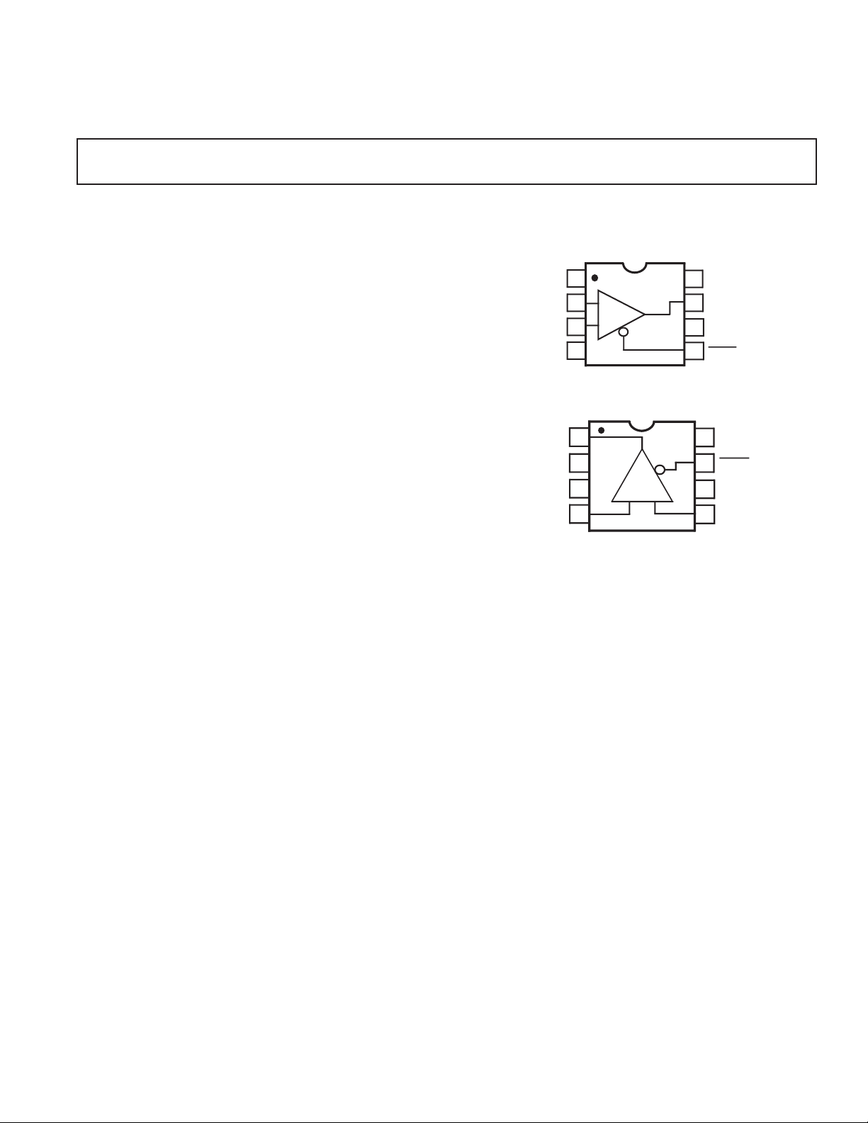
CONNECTION DIAGRAMS
8-Pin Plastic Mini-DIP (N)
and Cerdip (Q) Packages
+V
1
S
+IN
2
–IN
3
–V
45
S
AD790
+
–
8-Pin SOIC (R) Package
V
LOGIC
+V
+IN
1
2
3
S
4
AD790
+
–
OUTPUT
Comparator
AD790
V
8
LOGIC
OUTPUT
7
6
GROUND
LATCH
GROUND
8
7
LATCH
–V
6
S
5
–IN
PRODUCT DESCRIPTION
The AD790 is a fast (45 ns), precise voltage comparator, with a
number of features that make it exceptionally versatile and easy
to use. The AD790 may operate from either a single 5 V supply
or a dual ±15 V supply. In the single-supply mode, the AD790’s
inputs may be referred to ground, a feature not found in other
comparators. In the dual-supply mode it has the unique ability
of handling a maximum differential voltage of 15 V across its input terminals, easing their interfacing to large amplitude and
dynamic signals.
This device is fabricated using Analog Devices’ Complementary
Bipolar (CB) process—which gives the AD790’s combination
of fast response time and outstanding input voltage resolution
(1 mV max). To preserve its speed and accuracy, the AD790
incorporates a “low glitch” output stage that does not exhibit
the large current spikes normally found in TTL or CMOS output
stages. Its controlled switching reduces power supply disturbances
that can feed back to the input and cause undesired oscillations.
The AD790 also has a latching function which makes it suitable
for applications requiring synchronous operation.
The AD790 is available in five performance grades. The
AD790J and the AD790K are rated over the commercial temperature range of 0°C to 70°C. The AD790A and AD790B are
rated over the industrial temperature range of –40°C to +85°C.
The AD790S is rated over the military temperature range of
–55°C to +125°C.
PRODUCT HIGHLIGHTS
1. The AD790’s combination of speed, precision, versatility
and low cost makes it suitable as a general purpose comparator in analog signal processing and data acquisition systems.
2. Built-in hysteresis and a low-glitch output stage minimize the
chance of unwanted oscillations, making the AD790 easier to
use than standard open-loop comparators.
3. The hysteresis combined with a wide input voltage range
enables the AD790 to respond to both slow, low level (e.g.,
10 mV) signals and fast, large amplitude (e.g., 10 V) signals.
4. A wide variety of supply voltages is acceptable for operation
of the AD790, ranging from single 5 V to dual +5 V/–12 V,
± 5 V, or +5 V/± 15 V supplies.
5. The AD790’s power dissipation is the lowest of any comparator in its speed range.
6. The AD790’s output swing is symmetric between V
LOGIC
and ground, thus providing a predictable output under a
wide range of input and output conditions.
REV. C
Information furnished by Analog Devices is believed to be accurate and
reliable. However, no responsibility is assumed by Analog Devices for its
use, nor for any infringements of patents or other rights of third parties that
may result from its use. No license is granted by implication or otherwise
under any patent or patent rights of Analog Devices.
One Technology Way, P.O. Box 9106, Norwood, MA 02062-9106, U.S.A.
Tel: 781/329-4700 www.analog.com
Fax: 781/326-8703 © Analog Devices, Inc., 2002
Page 2

AD790–SPECIFICATIONS
DUAL SUPPLY
(Operation @ 25ⴗC and +VS = 15 V, –VS = –15 V, V
= 5 V unless otherwise noted.)
LOGIC
AD790J/A AD790K/B AD790S
Parameter Conditions Min Typ Max Min Typ Max Min Typ Max Unit
RESPONSE CHARACTERISTIC 100 mV Step
Propagation Delay, t
PD
5 mV Overdrive 40 45 40 45 40 45 ns
T
MIN
to T
MAX
45/50 45/50 60 ns
OUTPUT CHARACTERISTICS
Output HIGH Voltage, V
OH
1.6 mA Source 4.65 4.65 4.65
6.4 mA Source 4.3 4.45 4.3 4.45 4.3 4.45 V
Output LOW Voltage, V
OL
to T
T
MIN
MAX
1.6 mA Sink 0.35 0.35 0.35 V
4.3/4.3 4.3 4.3 V
6.4 mA Sink 0.44 0.5 0.44 0.5 0.44 0.5 V
T
INPUT CHARACTERISTICS
Offset Voltage
Hysteresis
1
2
to T
MIN
MAX
to T
T
MIN
MIN
to T
MAX
MAX
0.3 0.4 0.6 0.3 0.4 0.5 0.3 0.4 0.65 mV
T
0.5/0.5 0.5 0.5 V
0.2 1.0 0.05 0.25 0.2 1.0 mV
1.5 0.5 1.5 mV
Bias Current Either Input 2.5 5 1.8 3.5 2.5 5 µA
to T
T
MIN
MAX
6.5 4.5 7 µA
Offset Current 0.04 0.25 0.02 0.15 0.04 0.25 µA
to T
T
MIN
MAX
0.3 0.2 0.4 µA
Power Supply
Rejection Ratio DC V
± 20% 80 90 88 100 80 90 dB
S
to T
T
MIN
MAX
76 88 85 93 76 85 dB
Input Voltage Range
Differential Voltage V
≤± 15 V ⴞV
S
Common Mode –V
S
S
+VS–2 V –V
S
ⴞV
S
+VS–2 V –V
ⴞV
S
+VS–2 V V
V
S
Common Mode
Rejection Ratio –10 V<V
CM
80 95 88 105 80 95 dB
<+10 V
to T
T
MIN
MAX
76 90 85 100 76 88 dB
Input Impedance 20储220储220储2MΩ储pF
LATCH CHARACTERISTICS
Latch Hold Time, t
Latch Setup Time, t
LOW Input Level, V
H
S
IL
HIGH Input Level, V
T
to T
MIN
MIN
to T
MAX
MA X
IH
T
25 35 25 35 25 35 ns
510 510 510 ns
0.8 0.8 0.8 V
1.6 1.6 1.6 V
Latch Input Current 2.3 5 2.3 3.5 2.3 5 µA
T
SUPPLY CHARACTERISTICS
Diff Supply Voltage
3
Logic Supply T
V
T
to T
MIN
LOGIC
to T
MIN
to T
MIN
MAX
= 5 V
MAX
MAX
4.5 33 4.5 33 4.7 33 V
4.0 7 4.0 7 4.2 7 V
7 58µA
Quiescent Current
+V
–V
V
LOGIC
S
S
+VS = 15 V 8 10 8 10 8 10 mA
–VS = –15 V 4 5 4 5 4 5 mA
V
= 5 V 2 3.3 2 3.3 2 3.3 mA
LOGIC
Power Dissipation 242 242 242 mW
TEMPERATURE RANGE
Rated Performance T
NOTES
1
Defined as the average of the input voltages at the low to high and high to low transition points. Refer to Figure 6.
2
Defined as half the magnitude between the input voltages at the low to high and high to low transition points. Refer to Figure 6.
3
+VS must be no lower than (V
All min and max specifications are guaranteed. Specifications shown in boldface are tested on all production units at final test.
Specifications subject to change without notice.
–0.5 V) in any supply operating conditions, except during power up.
LOGIC
MIN
to T
MAX
0 to 70/–40 to +85 0 to 70/–40 to +85 –55 to +125 °C
–2–
REV. C
Page 3

AD790
SINGLE SUPPLY
(Operation @ 25ⴗC and +VS = V
= 5 V, –VS = 0 V unless otherwise noted.)
LOGIC
1
AD790J/A AD790K/B AD790S
Parameter Conditions Min Typ Max Min Typ Max Min Typ Max Unit
RESPONSE CHARACTERISTIC 100 mV Step
Propagation Delay, t
PD
5 mV Overdrive 45 50 45 50 45 50 ns
T
MIN
to T
MAX
50/60 50/60 65 ns
OUTPUT CHARACTERISTICS
Output HIGH Voltage, V
OH
1.6 mA Source 4.65 4.65 4.65
6.4 mA Source 4.3 4.45 4.3 4.45 4.3 4.45 V
Output LOW Voltage, V
OL
to T
T
MIN
MAX
1.6 mA Sink 0.35 0.35 0.35 V
4.3 4.3 4.3 V
6.4 mA Sink 0.44 0.5 0.44 0.5 0.44 0.5 V
T
INPUT CHARACTERISTICS
Offset Voltage
Hysteresis
2
3
to T
MIN
MAX
to T
T
MIN
MIN
to T
MAX
MAX
0.3 0.5 0.75 0.3 0.5 0.65 0.3 0.7 1.0 mV
T
0.5 0.5 0.5 V
0.45 1.5 0.35 0.6 0.45 1.5 mV
2.0 0.85 2.0 mV
Bias Current Either Input 2.7 5 2.0 3.5 2.7 5 µA
to T
T
MIN
MAX
7 58µA
Offset Current 0.04 0.25 0.02 0.15 0.04 0.25 µA
to T
T
MIN
MAX
0.3 0.2 0.4 µA
Power Supply
Rejection Ratio DC 4.5 V≤V
T
≤5.5 V 80 90 86 100 80 90 dB
S
MIN
to T
MAX
76/76 88 82 93 76 85 dB
Input Voltage Range
Differential Voltage ⴞV
Common Mode 0 +V
S
–2 V 0 +VS–2 V 0 +VS–2 V V
S
ⴞV
S
ⴞV
V
S
Input Impedance 20储220储220储2MΩ储pF
LATCH CHARACTERISTICS
Latch Hold Time, t
Latch Setup Time, t
LOW Input Level, V
H
S
IL
HIGH Input Level, V
T
to T
MIN
MIN
to T
MAX
MAX
IH
T
25 35 25 35 25 35 ns
510 510 510 ns
0.8 0.8 0.8 V
1.6 1.6 1.6 V
Latch Input Current 2.3 5 2.3 3.5 2.3 5 µA
T
SUPPLY CHARACTERISTICS
Supply Voltage
4
to T
MIN
MAX
T
MIN
to T
MAX
4.5 7 4.5 7 4.7 7 V
7 58µA
Quiescent Current 10 12 10 12 10 12 mA
Power Dissipation 60 60 60 mW
TEMPERATURE RANGE
Rated Performance T
NOTES
1
Pin 1 tied to Pin 8, and Pin 4 tied to Pin 6.
2
Defined as the average of the input voltages at the low to high and high to low transition points. Refer to Figure 6.
3
Defined as half the magnitude between the input voltages at the low to high and high to low transition points. Refer to Figure 6.
4
–VS must not be connected above ground.
All min and max specifications are guaranteed. Specifications shown in boldface are tested on all production units at final test.
Specifications subject to change without notice.
MIN
to T
MAX
0 to 70/–40 to +85 0 to 70/–40 to +85 –55 to +125 °C
REV. C
–3–
Page 4
AD790
–
ABSOLUTE MAXIMUM RATINGS
Supply Voltage . . . . . . . . . . . . . . . . . . . . . . . . . . . . . . . . ± 18 V
Internal Power Dissipation
2
. . . . . . . . . . . . . . . . . . . 500 mW
1, 2
Differential Input Voltage . . . . . . . . . . . . . . . . . . . . . ± 16.5 V
Output Short-Circuit Duration . . . . . . . . . . . . . . . . Indefinite
Storage Temperature Range
(N, R) . . . . . . . . . . . . . . . . . . . . . . . . . . . –65°C to +125°C
(Q) . . . . . . . . . . . . . . . . . . . . . . . . . . . . . . –65°C to +150°C
Lead Temperature Range (Soldering 60 sec) . . . . . . . . 300°C
Logic Supply Voltage . . . . . . . . . . . . . . . . . . . . . . . . . . . . . 7 V
NOTES
1
Stresses above those listed under “Absolute Maximum Ratings” may cause permanent damage to the device. This is a stress rating only and functional operation of
the device at these or any other conditions above those indicated in the operational
sections of this specification is not implied. Exposure to absolute maximum rating
conditions for extended periods may affect device reliability.
2
Thermal characteristics: plastic N-8 package: θJA = 90°C/watt; ceramic Q-8
package: θJA = 110°C/watt, θJC = 30°C/watt. SOIC (R-8) package: θJA = 160°C
watt; θJC = 42°C/watt.
+
+IN
–IN
0.1µF
2
3
15V
1
AD790
4
–
15V
5V
+
0.1µF
8
0.1µF
6
5
LATCH
(OPTIONAL)
510
7
Ω
OUTPUT
Figure 1. Basic Dual Supply
Configuration (N, Q Package Pinout)
ORDERING GUIDE
Temperature Package Package
Model Range Description Option
AD790JN 0°C to 70°C Plastic DIP N-8
AD790JR 0°C to 70°C SOIC SO-8
AD790JR-REEL 0°C to 70°C Reel
AD790JR-REEL7 0°C to 70°C SOIC R-8
AD790KN
*
0°C to 70°C Plastic DIP N-8
AD790AQ –40°C to +85°C Cerdip Q-8
AD790BQ
*
–40°C to +85°C Cerdip Q-8
AD790SQ –55°C to +125°C Cerdip Q-8
*
Not for new designs; obsolete April 2002.
For military processed devices, please refer to the standard Microcircuit Drawing (SMD) available at
www.dscc.dla.mil/programs/milspec/default.asp
SMD Part Number ADI Equivalent
5962-9150501MPA
*
Not for new designs; obsolete April 2002.
+IN
IN
2
3
*
+
1
AD790
4
5V
8
0.1µF
5
6
AD790 SQ/883
LATCH
(OPTIONAL)
510
7
Ω
OUTPUT
Figure 2. Basic Single Supply
Configuration (N, Q Package Pinout)
10kΩ
+15V
2
AD790
3
+5V
1
4
–15V
–
5V
VOLTAGE
SOURCE
0.1µF
1k
8
5
6
0.1µF
TEK
7904
7
SCOPE
PULSE
GENERATOR
–1.3V
–1.7V
HP8112
0.1µF
130Ω
HP2835
–5V
0.1µF
–100mV
25Ω
MPS
571
650Ω 400Ω 50Ω
–5mV
10Ω
Figure 3. Response Time Test Circuit (N, Q Package Pinout)
–4–
REV. C
Page 5

Typical Performace Characteristics–AD790
TPC 1. Propagation Delay vs.
Overdrive
TPC 4. Propagation Delay vs.
Source Resistance
5.0
4.9
4.8
4.7
4.6
4.5
4.4
OUTPUT LOW VOLTAGE – Volts
4.3
4.2
06410
28
I
SOURCE
TEMP = +25°C
– mA
TPC 2. Propagation Delay vs.
Load Capacitance
TPC 5. Propagation Delay vs.
Temperature
TPC 3. Propagation Delay vs.
Fanout (LSTTL and CMOS)
0.8
0.7
0.6
0.5
0.4
0.3
0.2
OUTPUT LOW VOLTAGE – Volts
0.1
0.0
06410
28
I
– mA
SINK
TPC 6. Output Low Voltage vs.
Sink Current
t
H
INPUT
t
S
t
PD
LATCH
OUTPUT
V
IH
TEMP = +25°C
0
V
IL
V
OH
V
OL
TPC 7. Output High Voltage vs.
Source Current
REV. C
TPC 8. Total Supply Current vs.
Temperature
–5–
tS = SETUP TIME
= HOLD TIME
t
H
t
= COMPARATOR RESPONSE TIME
PD
Figure 4. Latch Timing
Page 6

AD790
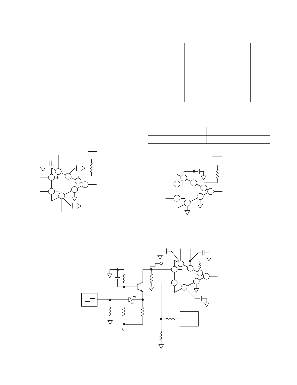
V
CIRCUIT DESCRIPTION
The AD790 possesses the overall characteristics of a standard
monolithic comparator: differential inputs, high gain and a logic
output. However, its function is implemented with an architecture which offers several advantages over previous comparator
designs. Specifically, the output stage alleviates some of the limitations of classic “TTL” comparators and provides a symmetric
output. A simplified representation of the AD790 circuitry is
shown in Figure 5.
V
LOGIC
+
+
IN
+
–
IN
–
GAIN STAGE
Av
A1
–
–
A2
+
OUTPUT STAGE
Q1
OUTPUT
Q2
GND
Figure 5. AD790 Block Diagram
The output stage takes the amplified differential input signal and
converts it to a single-ended logic output. The output swing is
defined by the pull-up PNP and the pull-down NPN. These produce inherent rail-to-rail output levels, compatible with CMOS
logic, as well as TTL, without the need for clamping to internal
bias levels. Furthermore, the pull-up and pull-down levels are
symmetric about the center of the supply range and are referenced off the V
supply and ground. The output stage has
LOGIC
nearly symmetric dynamic drive capability, yielding equal rise
and fall times into subsequent logic gates.
Unlike classic TTL or CMOS output stages, the AD790 circuit
does not exhibit large current spikes due to unwanted current
flow between the output transistors. The AD790 output stage
has a controlled switching scheme in which amplifiers A1 and
A2 drive the output transistors in a manner designed to reduce
the current flow between Q1 and Q2. This also helps minimize
the disturbances feeding back to the input which can cause
troublesome oscillations.
The output high and low levels are well controlled values defined
by V
(5 V), ground and the transistor equivalent Schottky
LOGIC
clamps and are compatible with TTL and CMOS logic requirements. The fanout of the output stage is shown in TPC 3 for
standard LSTTL or HCMOS gates. Output drive behavior vs.
capacitive load is shown in TPC 2.
HYSTERESIS
The AD790 uses internal feedback to develop hysteresis about
the input reference voltage. Figure 6 shows how the input offset
voltage and hysteresis terms are defined. Input offset voltage
) is the difference between the center of the hysteresis
(V
OS
range and the ground level. This can be either positive or negative. The hysteresis voltage (V
) is one-half the width of the
H
OUT
V
OH
V
OL
0
V
= HYSTERESIS VOLTAGE
H
VOS= INPUT OFFSET VOLTAGE
V
V
OS
H
GND
V
H
+
IN
+
IN
2
V
7
OUT
3
Figure 6. Hysteresis Definitions (N, Q Package Pinout)
hysteresis range. This built-in hysteresis allows the AD790 to
avoid oscillation when an input signal slowly crosses the ground
level.
SUPPLY VOLTAGE CONNECTIONS
The AD790 may be operated from either single or dual supply
voltages. Internally, the V
circuitry and the analog front-
LOGIC
end of the AD790 are connected to separate supply pins. If dual
supplies are used, any combination of voltages in which +V
V
– 0.5 V and –VS ≤ 0 may be chosen. For single supply
LOGIC
operation (i.e., +V
= V
S
), the supply voltage can be oper-
LOGIC
≥
S
ated between 4.5 V and 7 V. Figure 7 shows some other examples
of typical supply connections possible with the AD790.
BYPASSING AND GROUNDING
Although the AD790 is designed to be stable and free from
oscillations, it is important to properly bypass and ground the
power supplies. Ceramic 0.1 µF capacitors are recommended
and should be connected directly at the AD790’s supply pins.
These capacitors provide transient currents to the device during
comparator switching. The AD790 has three supply voltage
pins, +V
, –VS and V
S
. It is important to have a common
LOGIC
ground lead on the board for the supply grounds and the GND
pin of the AD790 to provide the proper return path for the
supply current.
LATCH OPERATION
The AD790 has a latch function for retaining input information
at the output. The comparator decision is “latched” and the
output state is held when Pin 5 is brought low. As long as Pin 5
is kept low, the output remains in the high or low state, and
does not respond to changing inputs. Proper capture of the
input signal requires that the timing relationships shown in
Figure 4 are followed. Pin 5 should be driven with CMOS or
TTL logic levels.
The output of the AD790 will respond to the input when Pin 5
is at a high logic level. When not in use, Pin 5 should be connected
to the positive logic supply. When using dual supplies, it is recommended that a 510 Ω resistor be placed in series with Pin 5
and the driving logic gate to limit input currents during powerup.
–6–
REV. C
Page 7

5V
5V
Applying the
L
O
A
D
2.7
PC BOARD
TRACE
AD790
1
2
3
4
5
6
7
8
0.1µF
5V
+
OUTPUT
R
SENSE
≈ 10mV/100mA
+V
S
510
Ω
Ω
AD790
0.1µF
+IN
–IN
+VS = +12V, –VS = 0V
+
12V
2
AD790
3
V
LOGIC
+
1
4
= +5V
0.1µF
510Ω
8
5
OUT
7
6
+IN
1
2
AD790
–IN
3
4
–
5V
+V
= +5V, –V
+
5V
8
= –5V, V
+IN
–IN
0.1µF
5
7
6
0.1µF
= +5V
1
2
AD790
3
–
15V
+VS = +5V, –VS = –15V
OUT
+
4
V
8
LOGIC
6
5
0.1µF
= +5V
0.1µF
OUT
7
Figure 7. Typical Power Supply Connections
(N, Q Package Pinout)
Window Comparator for Overvoltage Detection
The wide differential input range of the AD790 makes it suitable
for monitoring large amplitude signals. The simple overvoltage
detection circuit shown in Figure 8 illustrates direct connection
of the input signal to the high impedance inputs of the comparator
without the need for special clamp diodes to limit the differential
input voltage across the inputs.
The minus supply current is proportional to absolute temperature and compensates for the change in the sense resistance
with temperature. The width and length of the PC board trace
determine the resistance of the trace and consequently the trip
current level.
I
= 10 mV/R
LIMIT
R
= rho (trace length/trace width)
SENSE
SENSE
rho = resistance of a unit square of trace
0.1µF
+7.5V
+5V
+15V
1
3
AD790
2
4
–15V
V
IN
0.1µF
+15V +5V
1
3
AD790
–7.5V
2
Single Supply Ground Referred Overload Detector
The AD790 is useful as an overload detector for sensitive loads
that must be powered from a single supply. A simple ground
referenced overload detector is shown in Figure 8. The comparator senses a voltage across a PC board trace and compares
Figure 8. Overvoltage Detector
(N, Q Package Pinout)
4
–15V
8
8
6
6
0.1µF
5
0.1µF
0.1µF
5
0.1µF
510Ω
7
510Ω
7
SIGN 1 = HIGH
0 = LOW
OVERRANGE = 1
7432
that to a reference (trip) voltage established by the comparator’s
minus supply current through a 2.7 Ω resistor. This sets up a
10 mV reference level that is compared to the sense voltage.
Figure 9. Ground Referred Overload Detector Circuit
(N, Q Package Pinout)
Precision Full-Wave Rectifier
The high speed and precision of the AD790 make it suitable
for use in the wide dynamic range full-wave rectifier shown in
Figure 10. This circuit is capable of rectifying low level signals
as small as a few mV or as high as 10 V. Input resolution, propagation delay and op amp settling will ultimately limit the maximum
input frequency for a given accuracy level. Total comparator
plus switch delay is approximately 100 ns, which limits the
maximum input frequency to 1 MHz for clean rectification.
Ω
10k
+15V
0.1µF
10k
V
IN
0.1µF
+15V
3
AD790
2
1
4
–15V
+5V
8
0.1µF
5
6
0.1µF
510
20k
7
Ω
Ω
Ω
FET SWITCHES THE GAIN
FROM +1 TO –1
NMOS
FET
(R
ON
2
3
< 20 )
7
AD711
4
–15V
Ω
6
0.1µF
Figure 10. Precision Full-Wave Rectifier
(N, Q Package Pinout)
V
OUT
REV. C
–7–
–7–
Page 8

AD790
5V
–
5V
BIPOLAR
SIGNAL
INPUT
1k
Ω
STANDARD
SCHOTTKY
DIODE
*
A RESISTOR UP TO 10k MAYBE USED TO
REDUCE THE SOURCE AND SINK CURRENT OF
THE DRIVER. HOWEVER, THIS WILL SLIGHTLY
LOWER THE MAXIMUM USABLE CLOCK RATE.
2
3
Ω
+
4.7V
TTL
LEVEL
OUTPUT
0.3V
Ω
1
400 *
8
5
7
6
4
GND
Figure 11. A Bipolar to CMOS TTL Line Receiver (N, Q
Package Pinout)
Bipolar to CMOS/TTL
It is sometimes desirable to translate a bipolar signal (e.g.,
± 5 V) coming from a communications cable or another section
of the system to CMOS/TTL logic levels; such an application is
referred to as a line receiver. Previously, the interface to the
bipolar signal required either a dual (±) power supply or a reference voltage level about which the line receiver would switch.
The AD790 may be used in a simple circuit to provide a unique
capability: the ability to receive a bipolar signal while powered
from a single 5 V supply. Other comparators cannot perform
this task. Figure 11 shows a 1 kΩ resistor in series with the input
signal which is then clamped by a Schottky diode, holding the
input of the comparator at 0.4 V below ground. Although the
comparator is specified for a common mode range down to –V
,
S
(in this case ground) it is permissible to bring one of the inputs
a few hundred mV below ground. The comparator switches
around this level and produces a CMOS/TTL compatible swing.
The circuit will operate to switching frequencies of 20 MHz.
–8–
REV. C
Page 9

OUTLINE DIMENSIONS
Dimensions shown in inches and (mm).
AD790
8-Pin Plastic Mini-DIP (N-8) Package
8-Pin Cerdip (Q-8) Package
SOIC (SO-8) Package
REV. C
–9–
Page 10

AD790
Revision History
Location Page
Data Sheet changed from REV. B to REV. C.
Edits to FEATURES . . . . . . . . . . . . . . . . . . . . . . . . . . . . . . . . . . . . . . . . . . . . . . . . . . . . . . . . . . . . . . . . . . . . . . . . . . . . . . . . . . . . . 1
Edits to PRODUCT DESCRIPTION . . . . . . . . . . . . . . . . . . . . . . . . . . . . . . . . . . . . . . . . . . . . . . . . . . . . . . . . . . . . . . . . . . . . . . . . 1
Deleted METALIZATION PHOTOGRAPH . . . . . . . . . . . . . . . . . . . . . . . . . . . . . . . . . . . . . . . . . . . . . . . . . . . . . . . . . . . . . . . . . . 4
Edits to ORDERING GUIDE . . . . . . . . . . . . . . . . . . . . . . . . . . . . . . . . . . . . . . . . . . . . . . . . . . . . . . . . . . . . . . . . . . . . . . . . . . . . . . 4
–10–
REV. C
Page 11

–11–
Page 12

C00844–0–3/02(C)
–12–
PRINTED IN U.S.A.
 Loading...