

Page 1
5 V, 12-Bit, Serial 220 kSPS
a
FEATURES
Fast 12-Bit ADC with 220 kSPS Throughput Rate
8-Lead SOIC
Single 5 V Supply Operation
High-Speed, Flexible, Serial Interface that Also
Allows Interfacing to 3 V Processors
On-Chip Track/Hold Amplifier
Selection of Input Ranges
ⴞ10 V for AD7898-10
ⴞ2.5 V for AD7898-3
High Input Impedance
Low Power: 22.5 mW Max
GENERAL DESCRIPTION
The AD7898 is a fast 12-bit ADC that operates from a single
5 V supply and is housed in a small 8-lead SOIC package. The
part contains a successive approximation A/D converter, an onchip track/hold amplifier, an on-chip clock, and a high-speed
serial interface.
The AD7898 offers two modes of operation. In Mode 0, conversion is initiated by the CONVST input and the conversion
process is controlled by an internal clock oscillator. In this mode,
the serial interface consists of three wires and the AD7898 is
capable of throughput rates up to 220 kSPS. In Mode 1, the
conversion process is controlled by an externally-applied SCLK
with data being accessed from the part during conversion. In
this mode, the serial interface consists of three wires and the
AD7898 is capable of throughput rates up to 220 kSPS.
In addition to the traditional dc accuracy specifications such as
linearity and full-scale and offset errors, the AD7898 is specified
for dynamic performance parameters, including harmonic distortion and signal-to-noise ratio.
The part accepts an analog input range of ±10 V (AD7898-10)
and ± 2.5 V (AD7898-3), and operates from a single 5 V supply,
consuming only 22.5 mW max.
The part is available in an 8-lead small outline IC (SOIC).
ADC in an 8-Lead Package
AD7898
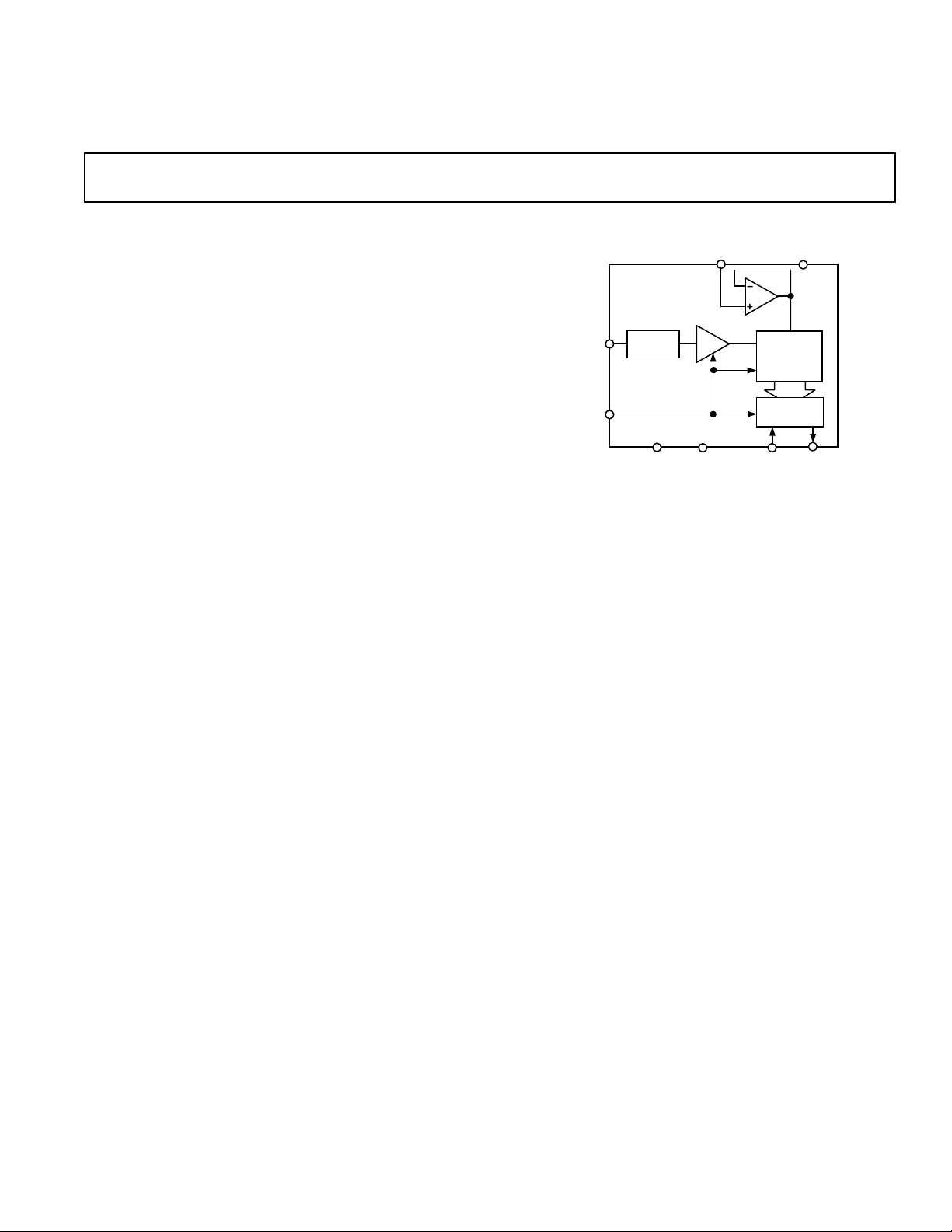
FUNCTIONAL BLOCK DIAGRAM
12-BIT
ADC
OUTPUT
REGISTER
SCLK
V
DD
SDATA
REF IN
AD7898
TRACK/HOLD
V
CONVST
PRODUCT HIGHLIGHTS
SIGNAL
IN
SCALING*
GND
*AD7898-10, AD7898-3
VDRIVE
1. Fast, 12-Bit ADC in 8-Lead Package
The AD7898 contains a 220 kSPS ADC, a track/hold amplifier, control logic, and a high-speed serial interface, all in an
8-lead package. This offers considerable space saving over
alternative solutions.
2. Low Power, Single Supply Operation
The AD7898 operates from a single 5 V supply and consumes only 22.5 mW. The V
function allows the serial
DRIVE
interface to connect directly to either 3 V or 5 V processor
systems independent of V
DD
.
3. Flexible, High-Speed Serial Interface
The part provides a flexible, high-speed serial interface that
has two distinct modes of operation. Mode 0 provides a threewire interface with data being accessed from the AD7898
when conversion is complete. Mode 1 offers a three-wire
interface with data being accessed during conversion.
4. Power-Down Mode
The AD7898 offers a proprietary power-down capability
when operated in Mode 1, making the part ideal for portable
or hand-held applications.
REV. 0
Information furnished by Analog Devices is believed to be accurate and
reliable. However, no responsibility is assumed by Analog Devices for its
use, nor for any infringements of patents or other rights of third parties
which may result from its use. No license is granted by implication or
otherwise under any patent or patent rights of Analog Devices.
One Technology Way, P.O. Box 9106, Norwood, MA 02062-9106, U.S.A.
Tel: 781/329-4700 World Wide Web Site: http://www.analog.com
Fax: 781/326-8703 © Analog Devices, Inc., 2000
Page 2

(VDD = 4.75 V to 5.25 V, V
1
AD7898–SPECIFICATIONS
to both Mode 0 and Mode 1 operations; TA = T
Parameter A Version
DYNAMIC PERFORMANCE
Signal to (Noise + Distortion) Ratio
T
to T
MIN
MAX
Total Harmonic Distortion (THD)
Peak Harmonic or Spurious Noise
Intermodulation Distortion (IMD)
2
2
2
2
71 dB min fIN = 30 kHz Sine Wave
–78 dB max fIN = 30 kHz Sine Wave
–89 dB typ fIN = 30 kHz Sine Wave
l
Unit Test Conditions/Comments
= 2.7 V to 5.25 V; REF IN = 2.5 V. Specifications apply
DRIVE
to T
MIN
, unless otherwise noted.)
MAX
fa = 29.1 kHz, fb = 29.9 kHz
2nd Order Terms –88 dB typ
3rd Order Terms –88 dB typ
Aperture Delay 20 ns typ
Aperture Jitter 75 ps typ
Full Power Bandwidth–AD7898-10 3.6 MHz typ @ 3 dB
Full Power Bandwidth–AD7898-3 4.7 MHz typ @ 3 dB
Full Power Bandwidth–AD7898-10 2.15 MHz typ @ 1 dB
Full Power Bandwidth–AD7898-3 2.4 MHz typ @ 1 dB
DC ACCURACY
Resolution 12 Bits
Minimum Resolution for Which 12 Bits
No Missing Codes are Guaranteed
Relative Accuracy
Differential Nonlinearity
Positive Full-Scale Error
Negative Full-Scale Error
2
2
2
2
± 1 LSB max
± 0.9 LSB max
± 3 LSB max
± 3 LSB max
Bipolar Zero Error ± 4 LSB max
ANALOG INPUT
AD7898-10
Input Voltage Range ±10 Volts
Input Resistance 24 kΩ min
AD7898-3
Input Voltage Range ±2.5 Volts
Input Resistance 5 kΩ min
REFERENCE INPUT
REF IN Input Voltage Range 2.375/2.625 V min/V max 2.5 V ± 5%
Input Current 1 µA max
Input Capacitance
2, 3
10 pF max
LOGIC INPUTS
Input High Voltage, V
Input Low Voltage, V
Input Current, I
Input Capacitance, C
INL
IN
IN
INH
2, 3
4
V
× 0.7 V min
DRIVE
V
× 0.3 V max
DRIVE
± 1 µA max Typically 10 nA, VIN = 0 V or V
10 pF max
LOGIC OUTPUTS
Output High Voltage, V
Output Low Voltage, V
Floating-State Leakage Current ±10 µA max
Floating-State Output Capacitance
OH
OL
2, 3
V
– 0.4 V min I
DRIVE
0.4 V max I
10 pF max
SOURCE
= 200 µA
SINK
= 200 µA; V
= 2.7 V to 5.25 V
DRIVE
Output Coding Two’s Complement
CONVERSION RATE
Mode 0 Operation 220 kSPS max With V
215 kSPS max With V
= 5 V ± 5%
DRIVE
= 2.7 V to 3.6 V
DRIVE
Mode 1 Operation 220 kSPS max
POWER REQUIREMENTS
V
DD
V
DRIVE
I
Static 4.25 mA max Digital Inputs @ V
DD
IDD Operational 4.5 mA max Digital Inputs @ V
4.75 to 5.25 V min to V max For Specified Performance
2.7 to 5.25 V min to V max For Specified Performance
DRIVE
DRIVE
Power Dissipation 22.5 mW max
POWER-DOWN MODE
I
@ 25°C5µA max Digital Inputs @ GND, VDD = 5 V ± 5%
DD
T
MIN
to T
MAX
20 µA max Digital Inputs @ GND, VDD = 5 V ± 5%
Power Dissipation @ 25°C (Operational) 25 µW max VDD = 5 V
NOTES
1
Temperature ranges are as follows: A Version: –40°C to +85°C.
2
See Terminology.
3
Sample tested @ 25°C to ensure compliance.
4
Operational with V
Specifications subject to change without notice.
= 2.35 V, with Input Low Voltage, V
DRIVE
= 0.4 V
INL
DRIVE
–2– REV. 0
Page 3

AD7898
TIMING SPECIFICATIONS
Parameter Limit at T
MIN
(VDD = 4.75 V to 5.25 V; V
1
noted.)
, T
Unit Description
MAX
= 2.7 V to 5.25 V; REF IN = 2.5 V; TA = T
DRIVE
MIN
to T
, unless otherwise
MAX
Mode 0 Operation
t
1
t
2
t
3
t
4
t
4
t
5
t
6
t
CONVERT
Mode 1 Operation
5
f
SCLK
40 ns min CONVST Pulsewidth
2
26
2
26
2
30
2
30
3
60
3
70
20 ns min Data Hold Time after Falling Edge of SCLK
4
50
ns min SCLK High Pulsewidth, V
ns min SCLK Low Pulsewidth, V
ns min SCLK High Pulsewidth V
ns min SCLK Low Pulsewidth V
= 5 V ± 5%
DRIVE
= 5 V ± 5%
DRIVE
= 2.7 V to 3.6 V
DRIVE
= 2.7 V to 3.6 V
DRIVE
ns max Data Access Time after Falling Edge of SCLK, V
ns max Data Access Time after Falling Edge of SCLK, V
ns max Bus Relinquish Time after Falling Edge of SCLK
3.3 µs
1 kHz min
= 5 V ± 5%
DRIVE
= 2.7 V to 3.6 V
DRIVE
3.7 MHz max
t
CONVERT
t
QUIET
t
2
3
t
3
3
t
4
t
5
t
6
t
7
4
t
8
16 × t
SCLK
4.33 µs max f
100 ns min Minimum Quiet Time Required between Conversions
70 ns min CS to SCLK Setup Time
40 ns max Delay from CS Until SDATA Three-State Disabled
80 ns max Data Access Time after SCLK Falling Edge
108 ns min SCLK High Pulsewidth
108 ns min SCLK Low Pulsewidth
60 ns min SCLK to Data Valid Hold Time
20 ns min SCLK Falling Edge to SDATA High Impedance
t
= 1/f
SCLK
= 3.7 MHz
SCLK
SCLK
60 ns max SCLK Falling Edge to SDATA High Impedance
t
POWER-UP
NOTES
1
Sample tested at 25°C to ensure compliance. All input signals are specified with tr = tf = 5 ns (10% to 90% of VDD) and timed from a voltage level of 1.6 V.
2
The SCLK maximum frequency is 15 MHz for Mode 0 operation for 220 kSPS throughput with V
The mark/space ratio for SCLK is specified for at least 40% high time (with corresponding 60% low time) or 40% low time (with corresponding 60% high time). As
the SCLK frequency is reduced, the mark/space ratio may vary, provided limits are not exceeded. Care must be taken when interfacing to account for the data access
time, t4, and the set-up time required for the users processor. These two times will determine the maximum SCLK frequency that the user’s system can operate with.
See Serial Interface section.
3
Measured with the load circuit of Figure 1 and defined as the time required for the output to cross 0.8 V or 2.0 V.
4
t6 and t8 are derived from the measured time taken by the data outputs to change 0.5 V when loaded with the circuit of Figure 1. The measured number is then extrapolated back to remove the effects of charging or discharging the 50 pF capacitor. This means that the time, t
relinquish time of the part and is independent of the bus loading.
5
Mark/Space ratio for the SCLK input is 40/60 to 60/40.
Specifications subject to change without notice.
4.33 µs max Power-Up Time from Power-Down Mode
= 5 V ± 5%, SCLK = 13 MHz with V
DRIVE
and t8, quoted in the timing characteristics is the true bus
6
= 2.7 V to 3.6 V.
DRIVE
–3–REV. 0
Page 4
AD7898
ABSOLUTE MAXIMUM RATINGS
(TA = 25°C unless otherwise noted)
1
VDD to GND . . . . . . . . . . . . . . . . . . . . . . . . . . –0.3 V to +7 V
Analog Input Voltage to GND
AD7898-10 . . . . . . . . . . . . . . . . . . . . . . . . . . . . . . . . ±17 V
AD7898-3 . . . . . . . . . . . . . . . . . . . . . . . . . . . . . . . . . ±10 V
Reference Input Voltage to GND . . . . –0.3 V to V
Digital Input Voltage to GND . . . . . . . –0.3 V to V
Digital Output Voltage to GND . . . . . –0.3 V to V
+ 0.3 V
DD
+ 0.3 V
DD
+ 0.3 V
DD
Operating Temperature Range
Commercial (A, B Versions) . . . . . . . . . . . –40°C to +85°C
Storage Temperature Range . . . . . . . . . . . –65°C to +150°C
Junction Temperature . . . . . . . . . . . . . . . . . . . . . . . . . . 150°C
SOIC Package, Power Dissipation . . . . . . . . . . . . . . . 450 mW
Thermal Impedance . . . . . . . . . . . . . . . . . . . . 170°C/W
θ
JA
Lead Temperature, Soldering
Vapor Phase (60 sec) . . . . . . . . . . . . . . . . . . . . . . . 215°C
Infrared (15 sec) . . . . . . . . . . . . . . . . . . . . . . . . . . . 220°C
ESD
AD7898-10 . . . . . . . . . . . . . . . . . . . . . . . . . . . . . . . . 2.5 kV
AD7898-3 . . . . . . . . . . . . . . . . . . . . . . . . . . . . . . . . . . 4 kV
NOTES
1
Stresses above those listed under Absolute Maximum Ratings may cause perma-
nent damage to the device. This is a stress rating; functional operation of the device
at these or any other conditions above those listed in the operational sections of this
specification is not implied. Exposure to absolute maximum rating conditions for
extended periods may affect device reliability.
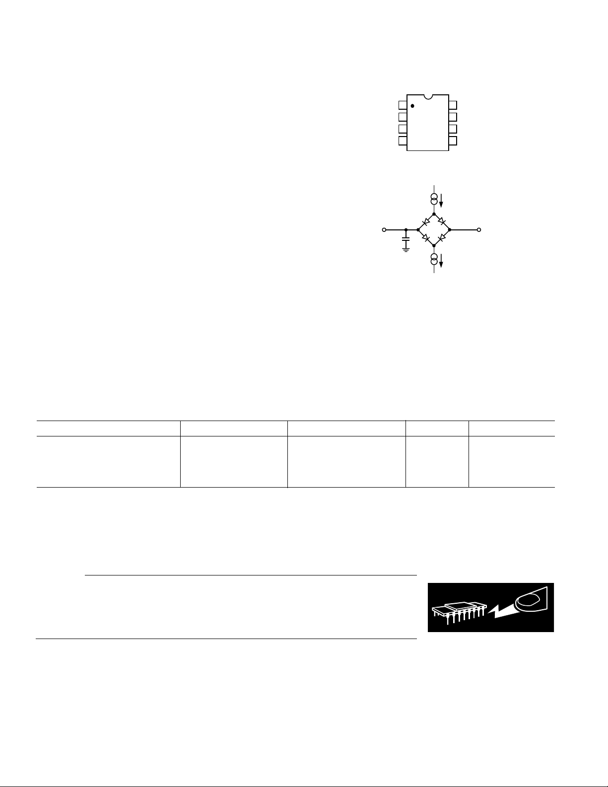
PIN CONFIGURATION
8
V
7
CS / CONVST
6
V
5
SDATA
I
OL
I
OH
DD
DRIVE
1.6V
OUTPUT
PIN
REF IN
TO
V
GND
SCLK
50pF
1
2
IN
3
4
C
L
AD7898
TOP VIEW
(Not to Scale)
200A
200A
Figure 1. Load Circuit for Digital Output Timing
Specifications
ORDERING GUIDE
Model Temperature Range Linearity Error (LSB)1SNR (dB) Package Option
AD7898AR-10 –40°C to +85°C ± 1 LSB 71 dB SO-8
AD7898AR-3 –40°C to +85°C ± 1 LSB 71 dB SO-8
EVAL-AD7898CB
EVAL-CONTROL BRD2
NOTES
1
Linearity Error refers to integral linearity error.
2
SO = SOIC.
3
This board is a complete unit allowing a PC to control and communicate with all Analog Devices evaluation boards ending in the CB designators.
3
CAUTION
ESD (electrostatic discharge) sensitive device. Electrostatic charges as high as 4000 V readily
accumulate on the human body and test equipment and can discharge without detection.
WARNING!
Although the AD7898 features proprietary ESD protection circuitry, permanent damage may
occur on devices subjected to high-energy electrostatic discharges. Therefore, proper ESD precautions are recommended to avoid performance degradation or loss of functionality.
ESD SENSITIVE DEVICE
2
–4– REV. 0
Page 5

AD7898
PIN FUNCTION DESCRIPTIONS
Pin Pin
No. Mnemonic Function
1 REF IN Voltage Reference Input. An external reference source should be connected to this pin to provide the
reference voltage for the AD7898’s conversion process. The REF IN input is buffered on-chip. The
nominal reference voltage for correct operation of the AD7898 is 2.5 V ± 5%. A 0.1 µF capacitor
should be placed on the REF IN pin.
2V
IN
3 GND Analog Ground. Ground reference for track/hold, comparator, digital circuitry, and DAC.
4 SCLK Serial Clock Input. An external serial clock is applied to this input to obtain serial data from the AD7898.
5 SDATA Serial Data Output. Serial data from the AD7898 is provided at this output. The serial data is clocked
6V
DRIVE
7 CS /CONVST Chip Select/Convert Start. This pin is CONVST, an edge-triggered logic input when in Mode 0 operation.
8V
DD
Analog Input Channel. The analog input range is ±10 V (AD7898-10) and ±2.5 V (AD7898-3).
When in Mode 0 operation, a new serial data bit is clocked out on the falling edge of this serial clock.
In Mode 0, data is guaranteed valid for 20 ns after this falling edge so that data can be accepted on the
falling edge when a fast serial clock is used. The serial clock input should be taken low at the end of
the serial data transmission. When in Mode 1 operation, SCLK also provides the serial clock for
accessing data from the part as in Mode 0, but this clock input is also used as the clock source for the
AD7898’s conversion process when in Mode 1.
out by the falling edge of SCLK, but the data can also be read on the falling edge of SCLK. This is
possible because data bit N is valid for a specified time after the falling edge of SCLK (data hold time).
Sixteen bits of serial data are provided with four leading zeros followed by the 12 bits of conversion data,
which is provided MSB first. On the 16th falling edge of SCLK, the SDATA line is held for the data
hold time and then is disabled (three-stated). Output data coding is two’s complement for the AD7898.
Logic Power Supply Input. The voltage supplied at this pin determines at what voltage the serial interface of the AD7898 will operate.
On the falling edge of this input, the track/hold goes into its hold mode, and conversion is initiated.
When in Mode 1 operation, this pin is Chip Select, an active low logic input. This input provides the
dual function of initiating conversions on the AD7898 and also frames the serial data transfer.
Power Supply Input, 5 V ± 5%.
–5–REV. 0
Page 6

AD7898
TERMINOLOGY
Signal to (Noise + Distortion) Ratio
This is the measured ratio of signal to (noise + distortion) at the
output of the A/D converter. The signal is the rms amplitude of
the fundamental. Noise is the rms sum of all nonfundamental
signals up to half the sampling frequency (f
/2), excluding dc.
S
The ratio is dependent upon the number of quantization levels
in the digitization process; the more levels, the smaller the quantization noise. The theoretical signal to (noise + distortion) ratio
for an ideal N-bit converter with a sine wave input is given by:
Signal to (Noise + Distortion) = (6.02 N + 1.76) dB
Thus for a 12-bit converter, this is 74 dB.
Total Harmonic Distortion
Total harmonic distortion (THD) is the ratio of the rms sum of
harmonics to the fundamental. For the AD7898, it is defined as:
THD dB
( ) log=
20
VV VVV
2
++ ++
223
42526
V
1
2
where V1 is the rms amplitude of the fundamental, and V2, V3,
V
, V5, and V6 are the rms amplitudes of the second through the
4
sixth harmonics.
Peak Harmonic or Spurious Noise
Peak harmonic or spurious noise is defined as the ratio of the
rms value of the next largest component in the ADC output
spectrum (up to f
/2 and excluding dc) to the rms value of the
S
fundamental. Normally, the value of this specification is determined by the largest harmonic in the spectrum, but for parts
where the harmonics are buried in the noise floor, it will be a
noise peak.
Intermodulation Distortion
With inputs consisting of sine waves at two frequencies, fa and
fb, any active device with nonlinearities will create distortion
products at sum and difference frequencies of mfa ± nfb where
m, n = 0, 1, 2, 3, etc. Intermodulation terms are those for which
neither m nor n are equal to zero. For example, the second order
terms include (fa + fb) and (fa – fb), while the third order terms
include (2 fa + fb), (2 fa – fb), (fa + 2 fb) and (fa – 2 fb).
The AD7898 is tested using the CCIF standard where two input
frequencies are used. In this case, the second and third order
terms are of different significance. The second order terms are
usually distanced in frequency from the original sine waves,
while the third order terms are usually at a frequency close to the
input frequencies. As a result, the second and third order terms
are specified separately. The calculation of the intermodulation
distortion is as per the THD specification where it is the ratio of
the rms sum of the individual distortion products to the rms
amplitude of the fundamental expressed in dBs.
Relative Accuracy
Relative accuracy or endpoint nonlinearity is the maximum
deviation from a straight line passing through the endpoints of
the ADC transfer function.
Differential Nonlinearity
This is the difference between the measured and the ideal
1 LSB change between any two adjacent codes in the ADC.
Positive Full-Scale Error (AD7898-10)
This is the deviation of the last code transition (01 . . . 110 to
01 . . . 111) from the ideal (4 × VREF – 3/2 LSB) after the
Bipolar Zero Error has been adjusted out.
Positive Full-Scale Error (AD7898-3)
This is the deviation of the last code transition (01 . . . 110 to
01 . . . 111) from the ideal (VREF – 3/2 LSB) after the Bipolar
Zero Error has been adjusted out.
Bipolar Zero Error (AD7898-10, AD7898-3)
This is the deviation of the midscale transition (all 0s to all 1s)
from the ideal AGND – 1/2 LSB.
Negative Full-Scale Error (AD7898-10)
This is the deviation of the first code transition (10 . . . 000 to
10 . . . 001) from the ideal (–4 × VREF + 1/2 LSB) after Bipolar Zero Error has been adjusted out.
Negative Full-Scale Error (AD7898-3)
This is the deviation of the first code transition (10 . . . 000 to
10 . . . 001) from the ideal (–VREF + 1/2 LSB) after Bipolar
Zero Error has been adjusted out.
Track/Hold Acquisition Time
Track/Hold acquisition time is the time required for the output
of the track/hold amplifier to reach its final value, within ±1/
2 LSB, after the end of conversion (the point at which the track/
hold returns to track mode). It also applies to situations where
there is a step input change on the input voltage applied to the
input of the AD7898. This means that the user must wait
V
IN
for the duration of the track/hold acquisition time after the end
of conversion, or after a step input change to V
, before start-
IN
ing another conversion to ensure that the part operates to
specification.
PSR (Power Supply Rejection)
Variations in power supply will affect the full-scale transition,
but not the converter’s linearity. Power Supply Rejection is the
maximum change in full-scale transition point due to change in
power-supply voltage from the nominal value.
–6– REV. 0
Page 7

Typical Performance Characteristics–AD7898
PERFORMANCE CURVES
TPC 1 shows a typical FFT plot for the AD7898 at 220 kSPS
sampling rate with a 30 kHz input frequency while operating in
Mode 0.
5
8192 POINT FFT
= 220kSPS
f
–15
–35
–55
SNR – dB
–75
–95
–115
FREQUENCY – kHz
SAMPLE
= 30kHz
f
IN
SINAD = 71.823dB
THD = –90.28dB
SFDR = –91.467dB
100806040200
TPC 1. Mode 0 Dynamic Performance
TPC 2 shows a typical FFT plot for the AD7898 at 220 kSPS
sampling rate with a 30 kHz input frequency while operating in
Mode 1.
5
8192 POINT FFT
= 220kSPS
f
–15
–35
–55
SNR – dB
–75
–95
SAMPLE
= 30kHz
f
IN
SINAD = 71.779dB
THD = –88.337dB
SFDR = –89.639dB
–20
–30
–40
–50
PSRR – dB
–60
–70
–80
INPUT FREQUENCY – kHz
80604020100
705030
TPC 3. PSRR vs. Supply Ripple Frequency
TPC 4 shows a graph of effective number of bits versus input
frequency while sampling at 220 kSPS.
11.9
11.8
11.7
11.6
11.5
11.4
EFFECTIVE NUMBER OF BITS
11.3
–115
FREQUENCY – kHz
100806040200
TPC 2. Mode 1 Dynamic Performance
TPC 3 shows the Power Supply Rejection Ratio versus supply
frequency for the AD7898. The power supply rejection ratio is
defined as the ratio of the power in the ADC output at full-scale
frequency f, to the power of a 100 mV sine wave applied to the
ADC V
supply of frequency fS.
DD
PSRR (dB) = 10 log (Pf/Pfs)
Pf = Power at frequency f in ADC output, Pfs = power at fre-
quency fs coupled on to the ADC V
100 mV peak-to-peak sine wave is coupled onto the V
supply input. Here a
DD
DD
supply.
100 nF decoupling was used on the supply.
–7–REV. 0
11.2
INPUT FREQUENCY – kHz
60
1008040200
TPC 4. Effective Number of Bits vs. Input Frequency at
220 kSPS
The effective number of bits for a device can be calculated from
its measured Signal to (Noise + Distortion) Ratio (see Terminology section). TPC 4 shows a typical plot of effective number
of bits versus frequency for the AD7898 from dc to f
SAMPLE/2
.
The sampling frequency is 220 kSPS.
The formula for Signal to (Noise + Distortion) Ratio is related
to the resolution or number of bits in the converter. Rewriting
the formula, below, gives a measure of performance expressed in
effective number of bits (N):
N = (SNR – 1.76)/6.02
where SNR is Signal to (Noise + Distortion) Ratio.
Page 8

AD7898
–40
–45
–50
–55
–60
SINAD – dB
–65
–70
–75
VDD = V
INPUT FREQUENCY – kHz
DRIVE
VDD = V
= 4.75V
VDD = 5.0V, V
DRIVE
= 5.25V
DRIVE
= 3.0V
100010010
TPC 5. SINAD vs. Input Frequency at 220 kSPS
TPC 5 shows a graph of Signal to (Noise + Distortion)
ratio versus Input Frequency for various supply voltages
while sampling at 220 kSPS. The on-chip track-and-hold
can accommodate frequencies up to 4.7 MHz for AD7898-3,
and up to 3.6 MHz for AD7898-10, making the AD7898 ideal
for subsampling applications.
Noise
In an A/D converter, noise exhibits itself as a code uncertainty
in dc applications, and as the noise floor (in an FFT, for
example) in ac applications. In a sampling A/D converter like
the AD7898, all information about the analog input appears in
the baseband, from dc to half the sampling frequency. The input
bandwidth of the track/hold exceeds the Nyquist bandwidth
and, therefore, an antialiasing filter should be used to remove
unwanted signals above f
/2 in the input signal in applications
S
where such signals exist.
TPC 6 shows a histogram plot for 8192 conversions of a dc
input using the AD7898. The analog input was set at the center
of a code transition. It can be seen that almost all the codes
appear in one output bin, indicating very good noise performance from the ADC.
6500
6000
5500
5000
4500
4000
3500
3000
2500
2000
1500
1000
500
0
2050
204920482047204620452044
TPC 6. Histogram of 8192 Conversions of a DC Input
CONVERTER DETAILS
The AD7898 is a fast, 12-bit single supply A/D converter. It
provides the user with signal scaling, track/hold, A/D converter,
and serial interface logic functions on a single chip. The A/D
converter section of the AD7898 consists of a conventional
successive-approximation converter based around an R-2R
ladder structure. The signal scaling on the AD7898-10 and
AD7898-3 allows the part to handle ±10 V and ±2.5 V input
signals, respectively, while operating from a single 5 V supply.
The part requires an external 2.5 V reference. The reference
input to the part is buffered on-chip. The AD7898 has two
operating modes, an internal clocking mode using an on-chip
oscillator and an external clocking mode using the SCLK as
the master clock. The latter mode features a power-down
mechanism. These modes are discussed in more detail in the
Operating Modes section.
A major advantage of the AD7898 is that it provides all of the
above functions in an 8-lead SOIC package. This offers the user
considerable spacing saving advantages over alternative solutions.
The AD7898 consumes only 22.5 mW maximum, making it
ideal for battery-powered applications.
In Mode 0 operation, conversion is initiated on the AD7898 by
pulsing the CONVST input. On the falling edge of CONVST,
the on-chip track/hold goes from track to hold mode, and the
conversion sequence is started. The conversion clock for the
part is generated internally using a laser-trimmed clock oscillator circuit. Conversion time for the AD7898 is 3.3 µs, and the
quiet time is 0.1 µs. To obtain optimum performance from the
part in Mode 0, the read operation should not occur during the
conversion.
In Mode 1 operation, conversion is initiated on the AD7898 by
the falling edge of CS. Sixteen SCLK cycles are required to
complete the conversion and access the conversion result, after
which time CS may be brought high. The internal oscillator is
not used as the conversion clock in this mode as the SCLK is
used instead. The maximum SCLK frequency is 3.7 MHz in
Mode 1 providing a minimum conversion time of 4.33 µs. As in
Mode 0, another conversion should not be initiated during the
quiet time after the end of conversion.
Both of these modes of operation allow the part to operate
at throughput rates up to 220 kHz and achieve data sheet
specifications.
CIRCUIT DESCRIPTION
Analog Input Section
The AD7898 is offered as two part types: the AD7898-10,
which handles a ±10 V input voltage range; the AD7898-3,
which handles input voltage range ±2.5 V.
VREF
V
AGND
IN
R1
AD7898-10/AD7898-3
TO ADC
REFERENCE
CIRCUITRY
R2
R3
TO INTERNAL
COMPARATOR
TRACK/HOLD
Figure 2. Analog Input Structure
–8– REV. 0
Page 9

AD7898
INPUT FREQUENCY – kHz
THD – dB
–20
–40
–80
100010
0
–10
–60
–100
100
–30
–70
–50
–90
VDD = V
DRIVE
= 4.75V
VDD = V
DRIVE
= 5.25V
VDD = 5.0V, V
DRIVE
= 3.0V
Figure 2 shows the analog input section for the AD7898-10
and AD7898-3. The analog input range of the AD7898-10 is
± 10 V into an input resistance of typically 30 kΩ. The analog
input range of the AD7898-3 is ±2.5 V into an input resistance
of typically 6 kΩ. This input is benign, with no dynamic charging currents, as the resistor stage is followed by a high input
impedance stage of the track/hold amplifier. For the AD7898-10,
R1 = 30 kΩ, R2 = 7.5 kΩ and R3 = 10 kΩ. For the AD7898-3,
R1 = R2 = 6.5 kΩ and R3 is open circuit.
For the AD7898-10 and AD7898-3, the designed code transitions occur midway between successive LSB values (i.e., 1/2 LSB,
3/2 LSBs, 5/2 LSBs . . .). Output coding is two’s complement
binary with 1 LSB = FS/4096. For the AD7898-10 1 LSB = 20/
4096 = 4.88 mV. For the AD7898-3 1 LSB = 5/4096 = 1.22 mV.
The ideal input/output coding for the AD7898-10 and AD78983 is shown in Table I.
Table I. Ideal Input/Output Code Table for the AD7898-10/-3
Digital Output
Analog Input
+FSR/2 – 3/2 LSB
l
2
Code Transition
011 . . . 110 to 011 . . . 111
+FSR/2 – 5/2 LSBs 011 . . . 101 to 011 . . . 110
+FSR/2 – 7/2 LSBs 011 . . . 100 to 011 . . . 101
AGND + 3/2 LSB 000 . . . 001 to 000 . . . 010
AGND + 1/2 LSB 000 . . . 000 to 000 . . . 001
AGND – 1/2 LSB 111 . . . 111 to 000 . . . 000
AGND – 3/2 LSB 111 . . . 110 to 111 . . . 111
–FSR/2 + 5/2 LSBs 100 . . . 010 to 100 . . . 011
–FSR/2 + 3/2 LSBs 100 . . . 001 to 100 . . . 010
–FSR/2 + 1/2 LSB 100 . . . 000 to 100 . . . 001
NOTES
1
FSR is full-scale range = 20 V (AD7898-10) and = 5 V (AD7898-3) with
REF IN = 2.5 V.
2
1 LSB = FSR/4096 = 4.883 mV (AD7898-10) and 1.22 mV (AD7898-3) with
REF IN = 2.5 V.
–60
–65
–70
–75
THD – dB
–80
–85
–90
f
IN
= 10k⍀
f
SOURCE IMPEDANCE – ⍀
= 50k⍀
IN
f
IN
= 25k⍀
f
= 110k⍀
IN
1k
Figure 3. THD vs. Source Impedance for Various Analog
Input Frequencies
Figure 3 shows a graph of THD versus Source Impedance for
different analog input frequencies when using a supply voltage
of 5 V, V
of 5 V, and sampling at a rate of 220 kSPS.
DRIVE
Source impedance has a minimal effect on THD because of the
resistive ladder structure of the input section of the ADC. Figure 4
shows a graph of THD versus Analog input frequency for various supply voltages while sampling at 220 kSPS.
Figure 4. THD vs. Analog Input Frequency for Various
Supply Voltages
Acquisition Time
The track-and-hold amplifier enters its tracking mode on the
falling 14th SCLK edge after the CS falling edge for Mode 1
operation. The time required for the track-and-hold amplifier to
acquire an input signal will depend on how quickly the 9.1 pF
sampling capacitance is charged. With zero source impedance
on the analog input, two SCLK cycles plus t
QUIET
will always
be sufficient to acquire the signal to the 12-bit level. With an
SCLK frequency of 3.7 MHz, the acquisition time would be
2 × (270 ns) + t
QUIET.
The acquisition time required is calculated using the following
formula:
t
= 10 × (RC)
ACQ
where R is the resistance seen by the track-and-hold amplifier
looking back on the input e.g., for AD7898-10 R = 3.75 kΩ and
for AD7898-3 R = 3.25 kΩ. The sampling capacitor has a value
of 9.1 pF. Theoretical acquisition times would be 340 ns for
AD7898-10, and 295 ns for AD7898-3. These theoretical values
do not include t
or track propagation delays in the part,
QUIET
typical values would be 520 ns for the AD7898-10 and 450 ns
for the AD7898-3.
10k10010
–9–REV. 0
Page 10

AD7898
TYPICAL CONNECTION DIAGRAM
Figure 5 shows a typical connection diagram for the AD7898.
The GND pin is connected to the analog ground plane of the
system. REF IN is connected to a decoupled 2.5 V supply from
a reference source, the AD780. This provides the analog reference for the part. The AD7898 is connected to a V
of 5 V,
DD
the serial interface is connected to a 3 V microprocessor. The
pin of the AD7898 is connected to the same 3 V supply
V
DRIVE
as the microprocessor to allow a 3 V logic interface. The conversion result from the AD7898 is output in a 16-bit word with
four leading zeros followed by the MSB of the 12-bit result. For
applications where power consumption is of concern, the powerdown mode should be used between conversions or bursts of
several conversions to improve power performance. See Modes
of Operation section.
ⴞ2.5V OR
ⴞ10V
INPUT
V
DD
V
IN
GND
0.1F
10F
AD7898
REF IN
0.1F
SCLK
SDATA
CS/CONVST
V
DRIVE
2.5V
AD780
5V
SUPPLY
SERIAL
INTERFACE
10F 0.1F
C/P
3V
SUPPLY
When in operating in Mode 1, the falling edge of CS will put
track-and-hold into hold mode. On the 14th SCLK falling edge
after the falling edge of CS, the track-and-hold will go back into
track (see Serial Interface section). The acquisition time of the
track/hold amplifier begins at this point.
Reference Input
The reference input to the AD7898 is buffered on-chip with a
maximum reference input current of 1 µA. The part is specified
with a 2.5 V reference input voltage. Errors in the reference
source will result in gain errors in the AD7898’s transfer function and will add to the specified full-scale errors on the part.
Suitable reference sources for the AD7898 include the AD780
and AD680 precision 2.5 V references.
SERIAL INTERFACE
The serial interface to the AD7898 consists of just three wires: a
serial clock input (SCLK), the serial data output (SDATA) and
a CS/CONVST input depending on the mode of operation.
This allows for an easy-to-use interface to most microcontrollers, DSP processors and shift registers. There is also a V
DRIVE
pin that allows the serial interface to connect directly to either
3 V or 5 V processor systems independent of V
. The serial
DD
interface operation is different in Mode 0 and Mode 1 operation
and is determined by which mode is selected. Upon power-up,
the default mode of operation is Mode 0. To select Mode 1
operation see the Mode Selection section. The serial interface
operation in Mode 0 and Mode 1 is described in detail in the
Operating Modes section.
Figure 5. Typical Connection Diagram
V
Feature
DRIVE
The AD7898 has the V
at which the Serial Interface operates. V
DRIVE
feature. V
controls the voltage
DRIVE
allows the ADC to
DRIVE
easily interface to both 3 V and 5 V processors. For example, if
the AD7898 were operated with a V
of 5 V, and the V
DD
DRIVE
pin could be powered from a 3 V supply. The AD7898 has good
dynamic performance with a V
of 5 V while still being able to
DD
interface to 3 V digital parts. Care should be taken to ensure
V
does not exceed VDD by more than 0.3 V (see Absolute
DRIVE
Maximum Ratings section).
Track/Hold Section
The track/hold amplifier on the analog input of the AD7898
allows the ADC to accurately convert an input sine wave of fullscale amplitude to 12-bit accuracy. The input bandwidth of the
track/hold is greater than the Nyquist rate of the ADC even
when the ADC is operated at its maximum throughput rate of
220 kSPS (i.e., the track/hold can handle input frequencies in
excess of 112 kHz). The track/hold amplifier acquires an input
signal to 12-bit accuracy in less than 0.5 µs.
The operation of the track/hold is essentially transparent to the
user. When in operating Mode 0, the track/hold amplifier goes
from its tracking mode to its hold mode at the start of conversion
(i.e., the falling edge of CONVST). The aperture time for the
track/hold (i.e., the delay time between the external CONVST
signal and the track/hold actually going into hold) is typically
15 ns. At the end of conversion (after 3.3 µs max), the part
returns to its tracking mode. The acquisition time of the track/
hold amplifier begins at this point.
OPERATING MODES
Mode 0 Operation
The timing diagram in Figure 6 shows the AD7898 operating in
Mode 0 where the falling edge of CONVST starts conversion
and puts the track/hold amplifier into its hold mode. The conversion is complete 3.3 µs max after the falling edge of CONVST,
and new data from this conversion is available in the output
register of the AD7898. A read operation accesses this data.
This read operation consists of 16 clock cycles and the length of
this read operation will depend on the serial clock frequency.
For the fastest throughput rate (with a serial clock of 15 MHz,
5 V operation) the read operation will take 1.066 µs. Once the
read operation has taken place, the required quiet time should
be allowed before the next falling edge of CONVST to optimize
the settling of the track/hold amplifier before the next conversion is initiated. A serial clock of less than 15 MHz can be used,
but this will, in turn, mean that the throughput time will increase.
The read operation consists of 16 serial clock pulses to the output shift register of the AD7898. After 16 serial clock pulses, the
shift register is reset, and the SDATA line is three-stated. If
there are more serial clock pulses after the 16th clock, the shift
register will be moved on past its reset state. However, the shift
register will be reset again on the falling edge of the CONVST
signal to ensure that the part returns to a known state after every
conversion cycle. As a result, a read operation from the output
register should not straddle the falling edge of CONVST as
the output shift register will be reset in the middle of the read
operation, and the data read back into the microprocessor will
appear invalid.
–10– REV. 0
Page 11

CONVST
AD7898
t
1
SCLK
CONVERSION IS
INITIATED AND
TRACK/HOLD GOES INTO
HOLD
t
CONVERT
= 3.3s
116
CONVERSION
ENDS
3.3s LATER
SERIAL READ
OPERATION
Figure 6. Serial Interface Timing Diagram Mode 0
t
2
SCLK 1 5 15234 16
SDATA
THREE-STATE
t
3
ZERO DB11 DB10 DB2 DB0Z DB1ZERO ZERO
FOUR LEADING ZEROS
t
5
t
4
Figure 7. Data Read Operation in Mode 0
Figure 7 shows the timing diagram for the read operation to the
AD7898 in Mode 0. The serial clock input (SCLK) provides
the clock source for the serial interface. Serial data is clocked
out from the SDATA line on the falling edge of this clock and is
valid on both the rising and falling edges of SCLK, depending
on the SCLK frequency used. The advantage of having the data
valid on both the rising and falling edges of the SCLK is that it
gives the user greater flexibility in interfacing to the part and
allows a wider range of microprocessor and microcontroller
interfaces to be accommodated. This also explains the two timing figures, t
The time, t
SCLK the next data bit becomes valid, whereas the time, t
and t5, that are quoted on the diagram.
4
, specifies how long after the falling edge of the
4
5
,
specifies for how long after the falling edge of the SCLK the
current data bit is valid. The first leading zero is clocked out on
the first rising edge of SCLK. Note that the first leading zero
will be valid on the first falling edge of SCLK even though the
data access time is specified at t
for the other bits (see Timing
4
Specifications). The reason the first bit will be clocked out faster
than the other bits is due to the internal architecture of the part.
Sixteen clock pulses must be provided to the part to access to
full conversion result. The AD7898 provides four leading zeros,
followed by the 12-bit conversion result starting with the MSB
(DB11). The last data bit to be clocked out on the fifteenth
falling clock edge is the LSB (DB0). On the 16th falling edge of
SCLK, the LSB (DB0) will be valid for a specified time to allow
100ns MIN
READ OPERATION
SHOULD END
100ns
PRIOR TO NEXT
FALLING EDGE OF
CONVST
14
OUTPUT
SERIAL
SHIFT
REGISTER
IS RESET
t
6
THREE-STATE
the bit to be read on the falling edge of the SCLK, then the
SDATA line is disabled (three-stated). After this last bit has
been clocked out, the SCLK input should return low and remain
low until the next serial data read operation. If there are extra
clock pulses after the 16th clock, the AD7898 will start over,
outputting data from its output register, and the data bus will no
longer be three-stated even when the clock stops. Provided the
serial clock has stopped before the next falling edge of CONVST,
the AD7898 will continue to operate correctly with the output
shift register being reset on the falling edge of CONVST. However, the SCLK line must be low when CONVST goes low in
order to correctly reset the output shift register.
The 16 serial clock input does not have to be continuous during
the serial read operation. The 16 bits of data (four leading zeros
and 12-bit conversion result) can be read from the AD7898 in a
number of bytes.
The AD7898 counts the serial clock edges to know which bit
from the output register should be placed on the SDATA output. To ensure that the part does not lose synchronization, the
serial clock counter is reset on the falling edge of the CONVST
input, provided the SCLK line is low. The user should ensure
that the SCLK line remains low until the end of the conversion.
When the conversion is complete, the output register will be
loaded with the new conversion result and can be read from the
ADC with 16 clock cycles of SCLK.
–11–REV. 0
Page 12

AD7898
CS
SCLK
SDATA
THREE-STATE
t
2
1
t
3
FOUR LEADING ZEROS
2
34
ZERO ZERO ZERO Z
t
CONVERT
t
6
56
t
4
DB11 DB10
t
5
DB9 DB0
Figure 8. Serial Interface Timing Diagram Mode 1
Mode 1 Operation
The timing diagram in Figure 8 shows the AD7898 operating in
Mode 1. The serial clock provides the conversion clock and also
controls the transfer of information from the AD7898 during
conversion.
CS initiates the data transfer and conversion process. The falling edge of CS puts the track-and-hold into hold mode, takes
the bus out of three-state and the analog input is sampled at
this point. The conversion is also initiated at this point and will
require 16 SCLK cycles to complete. On the 14th SCLK falling
edge the track-and-hold will go back into track. On the 16th
SCLK falling edge the SDATA line will go back into threestate. If the rising edge of CS occurs before 16 SCLKs have
elapsed then the conversion will be terminated and the SDATA
line will go back into three-state, otherwise SDATA returns to
three-state on the 16th SCLK falling edge as shown in Figure 8.
Sixteen serial clock cycles are required to perform the conversion process and to access data from the AD7898. CS going
low provides the first leading zero to be read in by the microcontroller or DSP. The remaining data is then clocked out by
subsequent SCLK falling edges beginning with the second leading zero, thus the first falling clock edge on the serial clock has
the first leading zero provided and also clocks out the second
leading zero. The final bit in the data transfer is valid on the
16th falling edge, having being clocked out on the previous (15th)
falling edge. It is also possible to read in data on each SCLK
rising edge, although the first leading zero will still have to be
read on the first SCLK falling edge after the CS falling edge.
Therefore the first rising edge of SCLK after the CS falling edge
would provide the second leading zero and the 15th rising SCLK
edge would have DB0 provided if the application requires data
to be read on each rising edge.
Mode Selection
Upon power-up, the default mode of operation of the AD7898
is Mode 0. The part will continue to operate in Mode 0 as outlined in the Mode 0 Operation section, provided an SCLK edge
is not applied to the AD7898 during the conversion time and
when CONVST is low. If an SCLK edge is applied to the
AD7898 during t
CONVERT
and when CONVST is low while in
Mode 0, the part will switch to operate in Mode 1 as shown in
Figure 9. The serial interface will now operate as described in
the Mode 1 operation section. The AD7898 will return to
Mode 0 operation from Mode 1 if CS is brought low and then
subsequently high without any SCLK edges provided while CS
15
14
t
7
16
t
8
t
QUIET
THREE-STATE
is low (see Figure 10). If any SCLK edges are applied to the
device while CS is low when in Mode 1, the part will remain in
Mode 1 and may or may not enter a power-down mode as
determined by the number of SCLKs applied, see Power-Down
Mode section.
If the part is operating in Mode 0 and a glitch occurs on the
SCLK line while CONVST is low, the part will enter Mode 1
and the conversion that was initiated by CONVST going low
will be terminated. The part will now be operating in Mode 1,
but Mode 0 signals will still be applied from the processor.
When CS goes low and no SCLK is applied, the part will revert
back to Mode 0 operation. This avoids accidental changing of
modes due to glitches on the SCLK line.
t
MODE 0
1
t
CONVERT
= 3.3s
CONVERSION
TERMINATES,
AD7898 ENTERS
MODE 1
CONVST
SCLK
CONVERSION IS
INITIATED IN
Figure 9. Entering Mode 1 from Mode 0
t
CS
SCLK
1
AD7898 ENTERS
MODE 0
Figure 10. Entering Mode 0 from Mode 1
Power-Down Mode
The power-down mode is only accessible when in Mode 1
operation. This mode is intended for use in applications where
slower throughput rates are required; either the ADC is powered down between each conversion, or a series of conversions
may be performed at a high throughput rate and the ADC is
powered down for a relatively long duration between these
bursts of several conversions. When the AD7898 is in powerdown, all analog circuitry is powered down.
–12– REV. 0
Page 13

CS
SCLK
1 16
234
11
AD7898
SDATA
Figure 11. Entering Power-Down when in Mode 1
THE PART BEGINS
TO POWER UP
CS
11116 161
SCLK
SDATA
INVALID DATA VALID DATA
Figure 12. Exiting Power-Down when in Mode 1
To enter power-down, the conversion process must be interrupted by bringing CS high anywhere after the fourth falling
edge of SCLK and before the 11th falling edge of SCLK as
shown in Figure 11. Once CS has been brought high in this
window of SCLK, then the part will enter power-down and the
conversion that was initiated by the falling edge of CS will be
terminated and SDATA will go back into three-state.
In order to exit this mode of operation and power the AD7898
up again, a dummy conversion is performed. On the falling edge
of CS the device will begin to power up, and will continue to
power up as long as CS is held low until after the falling edge of
the 11th SCLK. The device will be fully powered up once 16
SCLKs have elapsed and valid data will result from the next
conversion as shown in Figure 12. If CS is brought high before
the 11th falling edge of SCLK, the AD7898 will go back into
power-down. This avoids accidental power-up due to glitches
on the CS line or an inadvertent burst of eight SCLK cycles
while CS is low. So although the device may begin to power up
on the falling edge of CS, it will power down again on the rising
edge of CS as long as it occurs before the 11th SCLK falling edge.
Power-Up Times
The power-up time of the AD7898 is typically 4.33 µs, which
means that with any frequency of SCLK up to 3.7 MHz, one
dummy cycle will always be sufficient to allow the device to
power up. Once the dummy cycle is complete, the ADC will be
fully powered up and the input signal will be properly acquired.
The quiet time, t
, must still be allowed from the point at
QUIET
which the bus goes back into three-state after the dummy conversion, to the next falling CS edge.
When powering up from power-down mode at any SCLK frequency a dummy cycle is sufficient to power up the device and
fully acquire V
; it does not necessarily mean that a full dummy
IN
cycle of 16 SCLKs must always elapse to power up the device
and fully acquire V
the device and fully acquire V
. 4.33 µs would be sufficient to power up
IN
. If, for example, a 1 MHz SCLK
IN
frequency was applied to the ADC, the cycle time would be 16 µs.
THREE-STATE
THE PART IS FULLY
POWERED UP
In one dummy cycle, 16 µs, the part would be powered up and
V
fully acquired. However, after 4.33 µs with a 1 MHz SCLK
IN
just over four SCLK cycles would have elapsed. At this stage the
ADC would be fully powered up and the signal acquired. So, in
this case, CS could be brought high after the 11th SCLK falling
edge and brought low again after t
to initiate a new conversion.
QUIET
MICROPROCESSOR/MICROCONTROLLER INTERFACE
FOR MODE 0 OPERATION
The AD7898 provides a 3-wire serial interface that can be
used for connection to the serial ports of DSP processors and
microcontrollers. Figures 13 through 16 show the AD7898
interfaced to a number of different microcontrollers and DSP
processors. The AD7898 accepts an external serial clock and,
as a result, in all interfaces shown here, the processor/controller
is configured as the master, providing the serial clock with the
AD7898 configured as the slave in the system. The AD7898 has
no BUSY signal, therefore a read operation should be timed to
occur 3.3 µs after CONVST goes low.
8x51/L51 to AD7898 Interface
Figure 13 shows an interface between the AD7898 and the
8x51/L51 microcontroller. The 8x51/L51 is configured for its
Mode 0 serial interface mode. The diagram shows the simplest
form of the interface where the AD7898 is the only part connected to the serial port of the 8x51/L51 and, therefore, no
decoding of the serial read operations is required.
P3.0
8x51/L51
SDATA
AD7898
SCLKP3.1
Figure 13. 8x51/L51 to AD7898 Interface
–13–REV. 0
Page 14

AD7898
To chip-select the AD7898 in systems where more than one
device is connected to the 8x51/L51’s serial port, a port bit
configured as an output, from one of the 8x51/L51’s parallel
ports can be used to gate on or off the serial clock to the AD7898.
A simple AND function on this port bit and the serial clock from
the 8x51/L51 will provide this function. The port bit should be
high to select the AD7898 and low when it is not selected.
The AD7898 outputs the MSB first during a read operation,
while the 8xL51 expects the LSB first. Therefore, the data which
is read into the serial buffer needs to be rearranged before the
correct data format from the AD7898 appears in the accumulator.
The serial clock rate from the 8x51/L51 is limited to significantly less than the allowable input serial clock frequency with
which the AD7898 can operate. As a result, the time to read
data from the part will actually be longer than the conversion
time of the part. This means that the AD7898 cannot run at its
maximum throughput rate when used with the 8x51/L51.
68HC11/L11 to AD7898 Interface
An interface circuit between the AD7898 and the 68HC11/L11
microcontroller is shown in Figure 14. For the interface shown,
the 68L11 SPI port is used, and the 68L11 is configured in its
single-chip mode. The 68L11 is configured in the master mode
with its CPOL bit set to a logic zero and its CPHA bit set to a
logic one. As with the previous interface, the diagram shows the
simplest form of the interface where the AD7898 is the only part
connected to the serial port of the 68L11 and, therefore, no
decoding of the serial read operations is required.
SCK
68HC11/L11
MISO
SCLK
AD7898
SDATA
Figure 14. 68HC11/L11 to AD7898 Interface
Once again, to chip-select the AD7898 in systems where more
than one device is connected to the 68HC11’s serial port, a port
bit configured as an output from one of the 68HC11’s parallel
ports can be used to gate on or off the serial clock to the AD7898.
A simple AND function on this port bit and the serial clock
from the 68L11 will provide this function. The port bit should
be high to select the AD7898 and low when it is not selected.
The serial clock rate from the 68HC11/L11 is limited to significantly less than the allowable input serial clock frequency with
which the AD7898 can operate. As a result, the time to read
data from the part will actually be longer than the conversion
time of the part. This means that the AD7898 cannot run at its
maximum throughput rate when used with the 68HC11/L11.
ADSP-2103/ADSP-2105 to AD7898 Interface
An interface circuit between the AD7898 and the ADSP-2103/
ADSP-2105 DSP processor is shown in Figure 15. In the interface shown, the RFS1 output from the ADSP-2103/ADSP-2105’s
SPORT1 serial port is used to gate the serial clock (SCLK1) of
the ADSP-2103/ADSP-2105 before it is applied to the SCLK
input of the AD7898. The RFS1 output is configured for active
high operation. The interface ensures a noncontinuous clock for
the AD7898’s serial clock input with only 16 serial clock pulses
provided and the serial clock line of the AD7898 remaining low
between data transfers. A read operation should be timed to
occur 3.3 µs after CONVST goes low. The SDATA line from
the AD7898 is connected to the DR1 line of the ADSP-2103/
ADSP-2105’s serial port.
ADSP-2103/
ADSP-2105
RFS1
SCLK1
AD7898
SCLK
SDATADR1
Figure 15. ADSP-2103/ADSP-2105 to AD7898 Interface
The timing relationship between the SCLK1 and RFS1 outputs
of the ADSP-2103/ADSP-2105 are such that the delay between
the rising edge of the SCLK1 and the rising edge of an active
high RFS1 is up to 30 ns. There is also a requirement that data
must be set up 10 ns prior to the falling edge of the SCLK1 to
be read correctly by the ADSP-2103/ADSP-2105. The data
access time for the AD7898 is t
(5 V) from the rising edge of its
4
SCLK input. Assuming a 10 ns propagation delay through the
external AND gate, the high time of the SCLK1 output of the
ADSP-2105 must be ≥ (30 + 60 +10 +10) ns, i.e., ≥ 110 ns.
This means that the serial clock frequency with which the interface of Figure 15 can work is limited to 4.5 MHz. However,
there is an alternative method that allows for the ADSP-2105
SCLK1 to run at 5 MHz (the max serial clock frequency of the
SCLK1 output). The arrangement occurs when the first leading
zero of the data stream from the AD7898 cannot be guaranteed
to be clocked into the ADSP-2105 due to the combined delay of
the RFS signal and the data access time of the AD7898. In most
cases, this is acceptable because there will still be three leading
zeros followed by the 12 data bits.
Another alternative scheme is to configure the ADSP-2103/
ADSP-2105 so that it accepts an external noncontinuous serial
clock. In this case, an external noncontinuous serial clock is
provided that drives the serial clock inputs of both the ADSP2103/ADSP-2105 and the AD7898. In this scheme, the serial
clock frequency is limited to 15 MHz by the AD7898.
DSP56002/L002 to AD7898 Interface
Figure 16 shows an interface circuit between the AD7898 and
the DSP56002/L002 DSP processor. The DSP56002/L002 is
configured for normal mode asynchronous operation with gated
clock. It is also set up for a 16-bit word with SCK as gated clock
output. In this mode, the DSP56002/L002 provides sixteen
serial clock pulses to the AD7898 in a serial read operation.
Because the DSP56002/L002 assumes valid data on the first
falling edge of SCK, the interface is simply 2-wire as shown in
Figure 16.
DSP56002/L002
SCK
SDR
AD7898
SCLK
SDATA
Figure 16. DSP56002/L002 to AD7898 Interface
MICROPROCESSOR INTERFACING FOR MODE 1
The serial interface on the AD7898 for Mode 1 allows the parts
to be directly connected to a range of many different microprocessors. This section explains how to interface the AD7898 with
some of the more common microcontroller and DSP serial
interface protocols for Mode 1 operation.
–14– REV. 0
Page 15

AD7898
TMS320C5x/C54x to AD7898 Interface
The serial interface on the TMS320C5x/C54x uses a continuous serial clock and frame synchronization signal to synchronize
the data transfer operations with peripheral devices like the
AD7898. The CS input allows easy interfacing between the
TMS320C5x/C54x and the AD7898 without any glue logic
required. The serial port of the TMS320C5x/C54x is set up to
operate in burst mode with internal CLKX (TX serial clock)
and FSX (TX frame sync). The serial port control register (SPC)
must have the following setup: FO = 0, FSM = 1, MCM = 1,
and TXM = 1. The format bit, FO, may be set to 1 to set the
word length to 8 bits, in order to implement the power-down
modes on the AD7898.
The connection diagram is shown in Figure 17. It should be
noted that for signal processing applications, it is imperative that
the frame synchronization signal from the TMS320C5x/C54x
will provide equidistant sampling. The V
pin of the AD7898
DRIVE
takes the same supply voltage as that of the TMS320C5x/C54x.
This allows the ADC to operate at a higher voltage than the
serial interface, i.e., TMS320C5x/C54x, if necessary.
AD7898*
SCLK
SDATA
CS
V
DRIVE
*ADDITIONAL PINS OMITTED FOR CLARITY
TMS320C5x/C54x*
CLKX
CLKR
DR
FSX
FSR
V
DD
Figure 17. AD7898 to TMS320C5x Interface
AD7898 to ADSP-21xx Interface
The ADSP-21xx family of DSPs are interfaced directly to the
AD7898 without any glue logic required. The V
DRIVE
pin of the
AD7898 takes the same supply voltage as that of the ADSP-21xx.
This allows the ADC to operate at a higher voltage than the
serial interface, i.e., ADSP-21xx, if necessary.
The SPORT control register should be set up as follows:
TFSW = RFSW = 1, Alternate Framing
INVRFS = INVTFS = 1, Active Low Frame Signal
DTYPE = 00, Right Justify Data
SLEN = 1111, 16-Bit Data Words
ISCLK = 1, Internal Serial Clock
TFSR = RFSR = 1, Frame Every Word
IRFS = 0,
ITFS = 1.
To implement the power-down mode, SLEN should be set to
1001 to issue an 8-bit SCLK burst.
The connection diagram is shown in Figure 18. The ADSP-21xx
has the TFS and RFS of the SPORT tied together, with TFS
set as an output and RFS set as an input. The DSP operates in
Alternate Framing Mode and the SPORT control register is set
up as described. The Frame Synchronization signal generated
on the TFS is tied to CS and as with all signal processing applications equidistant sampling is necessary. However, in this example,
the timer interrupt is used to control the sampling rate of the
ADC and, under certain conditions, equidistant sampling may
not be achieved.
AD7898*
SCLK
SDATA
CS
V
DRIVE
*ADDITIONAL PINS OMITTED FOR CLARITY
ADSP-21xx*
SCLK
DR
RFS
TFS
V
DD
Figure 18. AD7898 to ADSP-21xx Interface
The Timer registers etc. are loaded with a value that will provide
an interrupt at the required sample interval. When an interrupt
is received, a value is transmitted with TFS/DT (ADC control
word). The TFS is used to control the RFS and hence the reading
of data. The frequency of the serial clock is set in the SCLKDIV
register. When the instruction to transmit with TFS is given, (i.e.,
AX0 = TX0), the state of the SCLK is checked. The DSP will
wait until the SCLK has gone high, low and high before transmission will start. If the timer and SCLK values are chosen such
that the instruction to transmit occurs on or near the rising edge
of SCLK, then the data may be transmitted or it may wait until
the next clock edge.
For example, the ADSP-2111 has a master clock frequency of
16 MHz. If the SCLKDIV register is loaded with the value 3, a
SCLK of 2 MHz is obtained, and eight master clock periods will
elapse for every 1 SCLK period. If the timer registers are loaded
with the value 803, 100.5 SCLKs will occur between interrupts
and subsequently between transmit instructions. This situation
will result in nonequidistant sampling as the transmit instruction
is occurring on an SCLK edge. If the number of SCLKs between
interrupts is a whole integer figure of N, equidistant sampling
will be implemented by the DSP.
AD7898 to DSP56xxx Interface
The connection diagram in Figure 19 shows how the AD7898
can be connected to the SSI (Synchronous Serial Interface) of
the DSP56xxx family of DSPs from Motorola. The SSI is operated in Synchronous Mode (SYN bit in CRB = 1) with internally
generated 1-bit clock period frame sync for both TX and RX
(bits FSL1 = 1 and FSL0 = 0 in CRB). Set the word length to
16 by setting bits WL1 = 1 and WL0 = 0 in CRA. To implement
the power-down mode on the AD7898 then the word length
can be changed to 8 bits by setting bits WL1 = 0 and WL0 = 0
in CRA. It should be noted that for signal processing applications, it is imperative that the frame synchronization signal
from the DSP56xxx will provide equidistant sampling. The
pin of the AD7898 takes the same supply voltage as that
V
DRIVE
of the DSP56xxx. This allows the ADC to operate at a higher
voltage than the serial interface, i.e., DSP56xxx, if necessary.
AD7898*
*ADDITIONAL PINS OMITTED FOR CLARITY
SCLK
SDATA
CS
V
DRIVE
SCK
SRD
SC2
DSP56xxx*
V
DD
Figure 19. AD7898 to DSP56xxx Interface
–15–REV. 0
Page 16

AD7898
AD7898 to MC68HC16 Interface
The Serial Peripheral Interface (SPI) on the MC68HC16 is
configured for Master Mode (MSTR = 1), Clock Polarity Bit
(CPOL) = 1 and the Clock Phase Bit (CPHA) = 0. The SPI is
configured by writing to the SPI Control Register (SPCR) (see
68HC16 user manual). The serial transfer will take place as a
16-bit operation when the SIZE bit in the SPCR register is set
to SIZE = 1. To implement the power-down modes with an
8-bit transfer set SIZE = 0. A connection diagram is shown in
Figure 20. The V
pin of the AD7898 takes the same sup-
DRIVE
ply voltage as that of the MC68HC16. This allows the ADC
to operate at a higher voltage than the serial interface, i.e.,
MC68HC16, if necessary.
OUTLINE DIMENSIONS
Dimensions shown in inches and (mm).
8-Lead SOIC
(SO-8)
AD7898*
SCLK
SDATA
CS
V
DRIVE
*ADDITIONAL PINS OMITTED FOR CLARITY
SCLK/PMC2
MISO/PMC0
SS/PMC3
Figure 20. AD7898 to MC68HC16 Interface
MC68HC16*
V
DD
C02145–2.5–10/00 (rev. 0)
0.1574 (4.00)
0.1497 (3.80)
PIN 1
0.0098 (0.25)
0.0040 (0.10)
SEATING
0.1968 (5.00)
0.1890 (4.80)
85
0.0500 (1.27)
BSC
PLANE
0.2440 (6.20)
0.2284 (5.80)
41
0.0192 (0.49)
0.0138 (0.35)
0.0688 (1.75)
0.0532 (1.35)
0.0098 (0.25)
0.0075 (0.19)
0.0196 (0.50)
0.0099 (0.25)
8ⴗ
0.0500 (1.27)
0ⴗ
0.0160 (0.41)
ⴛ 45ⴗ
PRINTED IN U.S.A.
–16–
REV. 0
 Loading...