

Page 1
LC2MOS 8-Channel, 12-Bit
+2.5V
REFERENCE
TRACK/HOLD
V
IN1A
V
IN1B
V
IN2A
V
IN2B
V
IN3A
V
IN3B
V
IN4A
V
IN4B
V
IN5A
V
IN5B
V
IN6A
V
IN6B
V
IN7A
V
IN7B
V
IN8A
V
IN8B
CONTROL LOGIC
WR CS RD EOC CONVST
MODE AGND
AGND DGND
CLOCK
VDDV
DD
AD7891
12-BIT
ADC
ADDRESS
DECODE
REF OUT/
REF IN
REF GND
STANDBY
M
U
X
DATA/
CONTROL
LINES
a
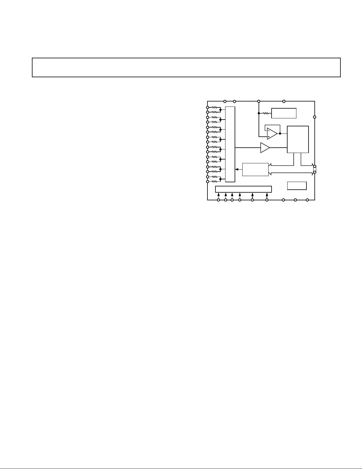
High Speed Data Acquisition System
AD7891
FEATURES
Fast 12-Bit ADC with 1.6 s Conversion Time
Eight Single-Ended Analog Input Channels
Overvoltage Protection on Each Channel
Selection of Input Ranges:
ⴞ5 V, ⴞ10 V for AD7891-1
0 to +2.5 V, 0 to +5 V, ⴞ2.5 V for AD7891-2
Parallel and Serial Interface
On-Chip Track/Hold Amplifier
On-Chip Reference
Single Supply, Low Power Operation (85 mW max)
Power-Down Mode (75 W typ)
APPLICATIONS
Data Acquisition Systems
Motor Control
Mobile Communication Base Stations
Instrumentation
GENERAL DESCRIPTION
The AD7891 is an eight-channel 12-bit data acquisition system
with a choice of either parallel or serial interface structure. The
part contains an input multiplexer, an on-chip track/hold amplifier, a high speed 12-bit ADC, a +2.5␣ V reference and a high
speed interface. The part operates from a single +5 V supply
and accepts a variety of analog input ranges across two models,
the AD7891-1 (±5␣ V and ±10␣ V) and the AD7891-2 (0 V to
+2.5 V, 0 V to +5␣ V and ±2.5␣ V).
The AD7891 provides the option of either a parallel interface or
serial interface structure determined by the MODE pin. The
part has standard control inputs and fast data access times for
both the serial and parallel interfaces which ensures easy interfacing to modern microprocessors, microcontrollers and digital
signal processors.
In addition to the traditional dc accuracy specifications such as
linearity, full-scale and offset errors, the part is also specified for
dynamic performance parameters including harmonic distortion
PRODUCT HIGHLIGHTS
1. The AD7891 is a complete monolithic 12-bit data acquisition
system combining an eight-channel multiplexer, 12-bit ADC,
+2.5␣ V reference and track/hold amplifier on a single chip.
2. The AD7891-2 features a conversion time of 1.6 µs and an
acquisition time of 0.4␣ µs. This allows a sample rate of
500␣ kSPS when sampling one channel and 62.5 kSPS when
channel hopping. These sample rates can be achieved using
either a software or hardware convert start. The AD7891-1
has an acquisition time of 0.6 µs when using a hardware
convert start and an acquisition time of 0.7 µs when using a
software convert start. These acquisition times allow sample
rates of 454.5 kSPS and 435 kSPS respectively for hardware
and software convert start.
3. Each channel on the AD7891 has overvoltage protection.
This means that an overvoltage on an unselected channel
does not affect the conversion on a selected channel. The
AD7891-1 can withstand overvoltages of ±17 V.
and signal-to-noise ratio.
Power dissipation in normal mode is 90 mW typical while in
One Technology Way, P.O. Box 9106, Norwood, MA 02062-9106, U.S.A.
Tel: 781/329-4700 World Wide Web Site: http://www.analog.com
Fax: 781/326-8703 © Analog Devices, Inc., 1998
the standby mode this is reduced to 75 µW typ. The part is
available in a 44-terminal plastic quad flatpack (PQFP) and a
44-lead plastic leaded chip carrier (PLCC).
REV. A
Information furnished by Analog Devices is believed to be accurate and
reliable. However, no responsibility is assumed by Analog Devices for its
use, nor for any infringements of patents or other rights of third parties
which may result from its use. No license is granted by implication or
otherwise under any patent or patent rights of Analog Devices.
FUNCTIONAL BLOCK DIAGRAM
Page 2

AD7891–SPECIFICATIONS
(VDD = +5 V ⴞ 5%, AGND = DGND = 0 V, REF IN = +2.5 V. All Specifications T
T
unless otherwise noted.)
MAX
MIN
to
ABY
Parameter Version1Version Version Units Test Conditions/Comments
DYNAMIC PERFORMANCE
2
Signal to (Noise + Distortion) Ratio
4
Sample Rate = 454.5 kSPS3 (AD7891-1),
500 kSPS
3
(AD7891-2). Any Channel
@ +25°C 707070dB min
T
to T
MIN
Total Harmonic Distortion
Peak Harmonic or Spurious Noise
Intermodulation Distortion
MAX
4
4
70 70 70 dB min
–78 –78 –78 dB max
4
–80 –80 –80 dB max
fa = 9 kHz, fb = 9.5 kHz
2nd Order Terms –80 –80 –80 dB typ
3rd Order Terms –80 –80 –80 dB typ
Channel-to-Channel Isolation
4
–80 –80 –80 dB max
DC ACCURACY Any Channel
Resolution 12 12 12 Bits
Minimum Resolution for Which
No Missing Codes are Guaranteed 12 12 12 Bits
Relative Accuracy
Differential Nonlinearity
Positive Full-Scale Error
Positive Full-Scale Error Match
4
4
4
±1 ±0.75 ±1 LSB max
±1 ±1 ±1 LSB max
±3 ±3 ±3 LSB max
4, 5
0.6 0.6 0.6 LSB typ 1.5 LSB max
Unipolar Offset Error ±3 ±3 ±3 LSB max Input Ranges of 0 V to +2.5␣ V, 0 V to +5␣ V
Unipolar Offset Error Match
Negative Full-Scale Error
Negative Full-Scale Error Match
5
4
0.1 0.1 0.1 LSB typ 1 LSB max
±3 ±3 ±3 LSB max Input Ranges of ±2.5␣ V, ±5␣ V, ±10␣ V
4, 5
0.6 0.6 0.6 LSB typ 1.5 LSB max
Bipolar Zero Error ±4 ±4 ±4 LSB max Input Ranges of ±2.5␣ V, ±5␣ V, ±10␣ V
Bipolar Zero Error Match
5
0.2 0.2 0.2 LSB typ 1.5 LSB max
ANALOG INPUTS
AD7891-1 Input Voltage Range
AD7891-1 V
AD7891-1 V
±5␣ ±5␣ ±5␣ Volts Input Applied to Both V
±10␣ ±10␣ ±10 Volts Input Applied to V
Input Resistance 7.5 7.5 7.5 kΩ min Input Range of ±5␣ V
INXA
Input Resistance 15 15 15 kΩ min Input Range of ±10␣ V
INXA
INXA
INXA
, V
and V
= AGND
INXB
INXB
AD7891-2 Input Voltage Range
AD7891-2 V
AD7891-2 V
0 to +2.5␣ 0 to +2.5␣ 0 to +2.5␣ ␣ Volts Input Applied to Both V
0 to +5␣ 0 to +5␣ 0 to +5␣ Volts Input Applied to V
±2.5␣ ± 2.5␣ ±2.5␣ Volts Input Applied to V
Input Resistance 1.5 1.5 1.5 kΩ min Input Ranges of ±2.5␣ V and 0 to +5␣ V
INXA
Input Current ±50 ±50 ±50 nA max Input Range of 0 V to +2.5␣ V
INXA
INXA
INXA
INXA
, V
, V
and V
= AGND
INXB
= REF IN
INXB
INXB
6
REFERENCE INPUT/OUTPUT
REF IN Input Voltage Range 2.375/2.625 2.375/2.625 2.375/2.625 V min/V max 2.5 V ± 5%
Input Impedance 1.6 1.6 1.6 kΩ min Resistor Connected to Internal Reference Node
Input Capacitance
5
10 10 10 pF max
REF OUT Output Voltage 2.5 2.5 2.5 V␣ nom
REF OUT Error @ +25°C ±10 ±10 ±10 mV max
T
MIN
to T
MAX
±20 ±20 ±20 mV max
REF OUT Temperature Coefficient 25 25 25 ppm/°C typ
REF OUT Output Impedance 5 5 5 kΩ nom See REF IN Input Impedance
LOGIC INPUTS
Input High Voltage, V
Input Low Voltage, V
Input Current, I
INL
INH
Input Capacitance,5 C
INH
IN
2.4 2.4 2.4 V min V
0.8 0.8 0.8 V max V
±10 ±10 ±10 µA max
10 10 10 pF max
= 5 V ± 5%
DD
= 5 V ± 5%
DD
–2– REV. A
Page 3

AD7891
WARNING!
ESD SENSITIVE DEVICE
ABY
Parameter Version1Version Version Units Test Conditions/Comments
LOGIC OUTPUTS
Output High Voltage, V
Output Low Voltage, V
OH
OL
4.0 4.0 4.0 V min I
0.4 0.4 0.4 V max I
DB11–DB0
Floating-State Leakage Current ±10 ±10 ±10 µA max
Floating-State Capacitance
5
15 15 15 pF max
Output Coding
Straight (Natural) Binary Data Format Bit of Control Register = 0
2s Complement Data Format Bit of Control Register = 1
CONVERSION RATE
Conversion Time 1.6 1.6 1.6 µs max
Track/Hold Acquisition Time 0.6 0.6 0.6 µs max AD7891-1 Hardware Conversion
0.7 0.7 0.7 µs max AD7891-1 Software Conversion
0.4 0.4 0.4 µs max AD7891-2
POWER REQUIREMENTS
V
DD
I
DD
+5 +5 +5 V nom ±5% for Specified Performance
Normal Mode 17 17 18 mA max
Standby Mode 80 80 80 µA max Logic Inputs = 0 V or V
Power Dissipation VDD = 5 V
Normal Mode 85 85 90 mW max Typically 70␣ mW
Standby Mode 400 400 400 µW max Typically 75 µW
NOTES
1
Temperature Ranges for the A and B Versions: –40°C to +85°C. Temperature Range for the Y Version: –55°C to +105°C.
2
The AD7891-1’s dynamic performance (THD and SNR) and the AD7891-2’s THD are measured with an input frequency of 10␣ kHz. The AD7891-2’s SNR is
evaluated with an input frequency of 100␣ kHz.
3
This throughput rate can only be achieved when the part is operated in the parallel interface mode. Maximum achievable throughput rate in the serial interface mode
is 357␣ kSPS.
4
See Terminology.
5
Sample tested during initial release and after any redesign or process change that may affect this parameter.
6
REF IN must be buffered before being applied to V
Specifications subject to change without notice.
INXB
.
SOURCE
= 1.6 mA
SINK
= 200 µA
DD
ABSOLUTE MAXIMUM RATINGS*
(T
= +25°C unless otherwise noted)
A
VDD to AGND . . . . . . . . . . . . . . . . . . . . . . . . . –0.3 V to +7 V
to DGND . . . . . . . . . . . . . . . . . . . . . . . . . –0.3 V to +7␣ V
V
DD
Analog Input Voltage to AGND
AD7891-1 . . . . . . . . . . . . . . . . . . . . . . . . . . . . . . . . . ±17␣ V
AD7891-2 . . . . . . . . . . . . . . . . . . . . . . . . . . . . –5 V, +10␣ V
Reference Input Voltage to AGND . . . . –0.3 V to V
Digital Input Voltage to DGND . . . . . . –0.3 V to V
Digital Output Voltage to DGND . . . . . –0.3 V to V
+ 0.3␣ V
DD
+ 0.3 V
DD
+ 0.3 V
DD
Operating Temperature Range
Commercial (A, B Version) . . . . . . . . . . . . – 40°C to +85°C
Automotive (Y Version) . . . . . . . . . . . . . . –55°C to +105°C
Storage Temperature Range . . . . . . . . . . . . –65°C to +150°C
Junction Temperature . . . . . . . . . . . . . . . . . . . . . . . . . +150°C
PQFP Package, Power Dissipation . . . . . . . . . . . . . . 450 mW
Thermal Impedance . . . . . . . . . . . . . . . . . . . . . . 95°C/W
θ
JA
Lead Temperature, Soldering
Vapor Phase (60 sec) . . . . . . . . . . . . . . . . . . . . . . . +215°C
Infrared (15 sec) . . . . . . . . . . . . . . . . . . . . . . . . . . +220°C
PLCC Package, Power Dissipation . . . . . . . . . . . . . . 500 mW
Thermal Impedance . . . . . . . . . . . . . . . . . . . . . . 55°C/W
θ
JA
Lead Temperature, Soldering
Vapor Phase (60 sec) . . . . . . . . . . . . . . . . . . . . . . . +215°C
Infrared (15 sec) . . . . . . . . . . . . . . . . . . . . . . . . . . +220°C
*Stresses above those listed under Absolute Maximum Ratings may cause perma-
nent damage to the device. This is a stress rating only; functional operation of the
device at these or any other conditions above those listed in the operational
sections of this specification is not implied. Exposure to absolute maximum rating
conditions for extended periods may affect device reliability.
CAUTION
ESD (electrostatic discharge) sensitive device. Electrostatic charges as high as 4000 V readily
accumulate on the human body and test equipment and can discharge without detection.
Although the AD7891 features proprietary ESD protection circuitry, permanent damage may
occur on devices subjected to high energy electrostatic discharges. Therefore, proper ESD
precautions are recommended to avoid performance degradation or loss of functionality.
–3–REV. A
Page 4
AD7891
TIMING CHARACTERISTICS
1, 2
Parameter A, B, Y Versions Units Test Conditions/Comments
t
CONV
1.6 µs max Conversion Time
Parallel Interface
t
1
t
2
t
3
t
4
t
5
t
6
t
7
t
8
3
t
9
4
t
10
0 ns min CS to RD/WR Setup Time
35 ns min Write Pulsewidth
25 ns min Data Valid to Write Setup Time
5 ns min Data Valid to Write Hold Time
0 ns min CS to RD/WR Hold Time
35 ns min CONVST Pulsewidth
55 ns min EOC Pulsewidth
35 ns min Read Pulsewidth
25 ns min Data Access Time after Falling Edge of RD
5 ns min Bus Relinquish Time after Rising Edge of RD
30 ns max
Serial Interface
t
t
t
t
t
t
t
t
t
11
12
13
14
15
16
17
18
18A
3
3
3
4
4
30 ns min RFS Low to SCLK Falling Edge Setup Time
20 ns max RFS Low to Data Valid Delay
25 ns min SCLK High Pulsewidth
25 ns min SCLK Low Pulsewidth
5 ns min SCLK Rising Edge to Data Valid Hold Time
15 ns max SCLK Rising Edge to Data Valid Delay
20 ns min RFS to SCLK Falling Edge Hold Time
0 ns min Bus Relinquish Time after Rising Edge of RFS
30 ns max
0 ns min Bus Relinquish Time after Rising Edge of SCLK
30 ns max
t
19
t
20
t
21
t
22
NOTES
1
Sample tested during initial release and after any redesign or process change that may affect this parameter. All input signals are measured with tr = tf = 1 ns (10% to
90% of +5 V) and timed from a voltage level of +1.6 V.
2
See Figures 2, 3 and 4.
3
Measured with the load circuit of Figure 1 and defined as the time required for an output to cross 0.8␣ V or 2.4␣ V.
4
These times are derived from the measured time taken by the data outputs to change 0.5␣ V when loaded with the circuit of Figure 1. The measured number is then
extrapolated back to remove the effects of charging or discharging the 50 pF capacitor. This means that the times quoted in the timing characteristics are the true bus
relinquish times of the part and as such are independent of external bus loading capacitances.
Specifications subject to change without notice.
20 ns min TFS Low to SCLK Falling Edge Setup Time
15 ns min Data Valid to SCLK Falling Edge Setup Time
10 ns min Data Valid to SCLK Falling Edge Hold Time
30 ns min TFS Low to SCLK Falling Edge Hold Time
1.6mA
TO
OUTPUT
PIN
50pF
200mA
+1.6V
Figure 1. Load Circuit for Access Time and Bus Relinquish Time
–4– REV. A
Page 5
AD7891
V
IN6A
AGND
EOC
NC
CONVST
CS
REF GND
NC
REF OUT/REF IN
V
DD
AGND
MODE
DB11/TEST
DB10/TEST
DB9/TFS
DB8/RFS
DB7/DATA IN
STANDBY
V
IN1A
DB6/SCLK
V
DD
DGND
DB5/A2/DATA OUT
DB3/A0
DB2/SWCON
DB1/SWSTBY
DB0/FORMAT
WR
RD
DB4/A1
V
IN1BVIN2AVIN2BVIN3AVIN3BVIN4AVIN4BVIN5AVIN5B
V
IN6B
V
IN7A
V
IN7B
V
IN8A
V
IN8B
NC = NO CONNECT
44 43 42 41 40 39 38 37 36 35 34
1
2
3
4
5
6
7
8
9
10
11
12 13 14 15 16 17 18 19 20 21 22
33
32
31
30
29
28
27
26
25
24
23
PIN 1
IDENTIFIER
TOP VIEW
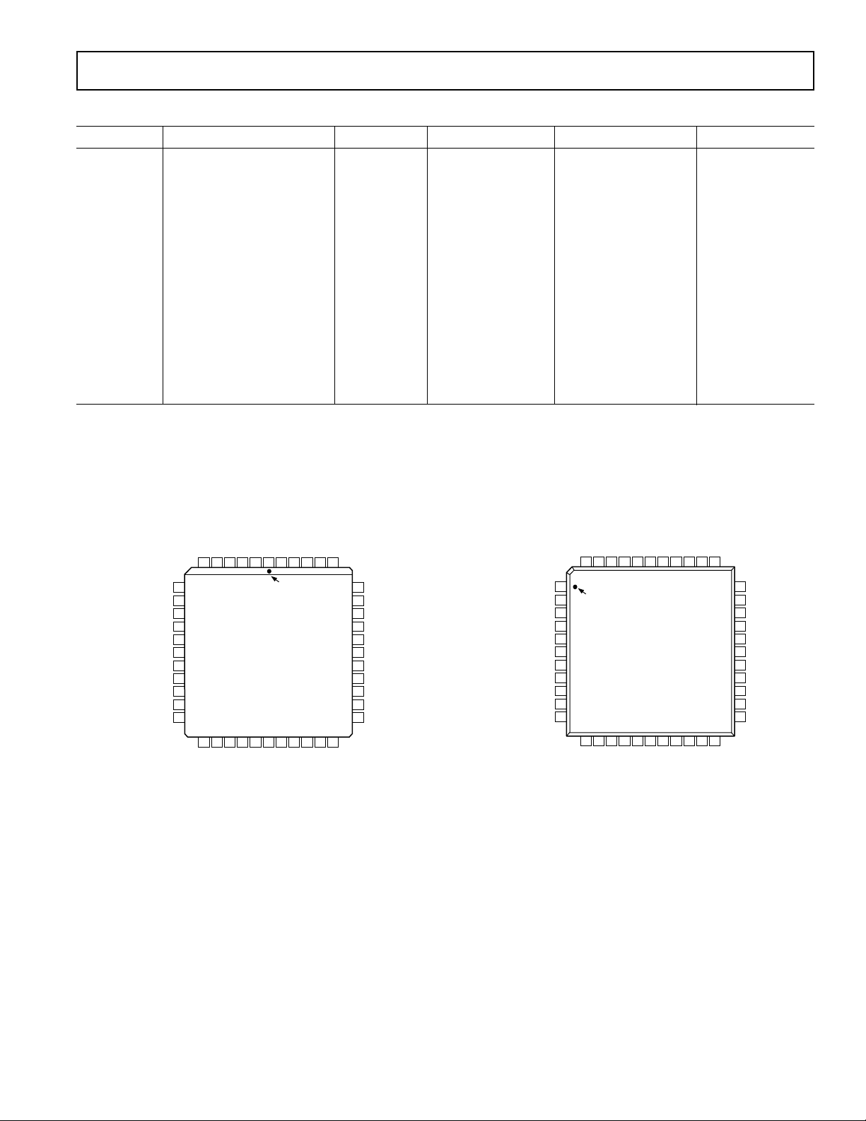
(Not to Scale)
AD7891 PQFP
ORDERING GUIDE
Model Input Ranges Sample Rate Relative Accuracy Temperature Range Package Options*
AD7891AS-1 ±5 V or ±10 V 454 kSPS ±1 LSB –40°C to +85°CS-44
AD7891AP-1 ±5 V or ±10 V 454 kSPS ±1 LSB –40°C to +85°C P-44A
AD7891BS-1 ±5 V or ±10 V 454 kSPS ±0.75 LSB –40°C to +85°CS-44
AD7891BP-1 ±5 V or ±10 V 454 kSPS ±0.75 LSB –40°C to +85°C P-44A
AD7891YS-1 ±5 V or ±10 V 454 kSPS ±1 LSB –55°C to +105°CS-44
AD7891YP-1 ±5 V or ±10 V 454 kSPS ±1 LSB –55°C to +105°C P-44A
AD7891AS-2 0 V to +5 V, 0 V to +2.5 V 500 kSPS ±1 LSB –40°C to +85°CS-44
or ±2.5 V
AD7891AP-2 0 V to +5 V, 0 V to +2.5 V 500 kSPS ±1 LSB –40°C to +85°C P-44A
or ±2.5 V
AD7891BS-2 0 V to +5 V, 0 V to +2.5 V 500 kSPS ±0.75 LSB –40°C to +85°CS-44
or ±2.5 V
AD7891BP-2 0 V to +5 V, 0 V to +2.5 V 500 kSPS ±0.75 LSB –40°C to +85°C P-44A
or ±2.5 V
AD7891YS-2 0 V to +5 V, 0 V to +2.5 V 500 kSPS ±1 LSB –55°C to +105°CS-44
or ±2.5 V
*S = Plastic Quad Flatpack (PQFP); P = Plastic Leaded Chip Carrier (PLCC).
PIN CONFIGURATIONS
REF GND
REF OUT/REF IN
DB11/TEST
DB10/TEST
DB9/TFS
DB8/RFS
DB7/DATA IN
NC = NO CONNECT
6 5 4 3 2 1 44 43 42 41 40
7
8
NC
9
10
V
DD
11
AGND
12
MODE
13
14
15
16
17
18 19 20 21 22 23 24 25 26 27 28
DB6/SCLK
PLCC
IN1A
IN1BVIN2AVIN2BVIN3AVIN3BVIN4AVIN4BVIN5AVIN5B
STANDBY
V
V
PIN 1
IDENTIFIER
AD7891 PLCC
TOP VIEW
(Not to Scale)
DD
V
DGND
DB3/A0
DB4/A1
DB2/SWCON
DB5/A2/DATA OUT
RD
WR
DB0/FORMAT
DB1/SWSTBY
39
38
37
36
35
34
33
32
31
30
29
V
IN6A
V
IN6B
V
IN7A
V
IN7B
V
IN8A
V
IN8B
AGND
EOC
NC
CONVST
CS
PQFP
–5–REV. A
Page 6

AD7891
TERMINOLOGY
Signal to (Noise + Distortion) Ratio
This is the measured ratio of signal to (noise + distortion) at the
output of the A/D converter. The signal is the rms amplitude of
the fundamental. Noise is the rms sum of all nonfundamental
signals up to half the sampling frequency (f
/2), excluding dc.
S
The ratio is dependent upon the number of quantization levels
in the digitization process; the more levels, the smaller the quantization noise. The theoretical signal to (noise +distortion) ratio
for an ideal N-bit converter with a sine wave input is given by:
Signal to (Noise + Distortion) = (6.02N + 1.76) dB
Thus for a 12-bit converter, this is 74␣ dB.
Total Harmonic Distortion
Total harmonic distortion (THD) is the ratio of the rms sum of
harmonics to the fundamental. For the AD7891 it is defined as:
2
THD dB
()
VVVVV
++++
=
20
223242526
log
V
1
where V1 is the rms amplitude of the fundamental and V2, V3,
, V5 and V6 are the rms amplitudes of the second through the
V
4
sixth harmonics.
Peak Harmonic or Spurious Noise
Peak harmonic or spurious noise is defined as the ratio of the
rms value of the next largest component in the ADC output
spectrum (up to f
/2 and excluding dc) to the rms value of the
S
fundamental. Normally, the value of this specification is determined by the largest harmonic in the spectrum, but for parts
where the harmonics are buried in the noise floor, it will be a
noise peak.
Intermodulation Distortion
With inputs consisting of sine waves at two frequencies, fa and
fb, any active device with nonlinearities will create distortion
products at sum and difference frequencies of mfa ± nfb where
m, n = 0, 1, 2, 3, etc. Intermodulation terms are those for which
neither m nor n are equal to zero. For example, the second
order terms include (fa + fb) and (fa – fb), while the third order
terms include (2fa + fb), (2fa – fb), (fa + 2fb) and (fa – 2fb).
The AD7891 is tested using the CCIF standard where two
input frequencies near the top end of the input bandwidth are
used. In this case, the second and third order terms are of different significance. The second order terms are usually distanced
in frequency from the original sine waves while the third order
terms are usually at a frequency close to the input frequencies.
As a result, the second and third order terms are specified separately. The calculation of the intermodulation distortion is as
per the THD specification where it is the ratio of the rms sum of
the individual distortion products to the rms amplitude of the
fundamental expressed in dBs.
Channel-to-Channel Isolation
Channel-to-channel isolation is a measure of the level of
crosstalk between channels. It is measured by applying a fullscale 20 kHz (AD7891-1) or 100 kHz (AD7891-2) sine wave
signal to one input channel and determining how much that
signal is attenuated in each of the other channels. The figure
given is the worst case across all eight channels.
Relative Accuracy
Relative accuracy or endpoint nonlinearity is the maximum
deviation from a straight line passing through the endpoints of
the ADC transfer function.
Differential Nonlinearity
This is the difference between the measured and the ideal 1 LSB
change between any two adjacent codes in the ADC.
Positive Full-Scale Error (AD7891-1, ±10 V and ±5 V,
AD7891-2, ±2.5 V)
This is the deviation of the last code transition (01. . .110 to
01. . .111) from the ideal 4 × REF IN – 3/2 LSB (AD7891-1
±10 V range), 2 × REF IN – 3/2 LSB (AD7891-1 ± 5 V range)
or REF IN – 3/2 LSB (AD7891-2, ±2.5 V range), after the
Bipolar Zero Error has been adjusted out.
Positive Full-Scale Error (AD7891-2, 0 V to 5 V and 0 V to
2.5 V)
This is the deviation of the last code transition (11. . .110 to
11. . .111) from the ideal 2 × REF IN – 3/2 LSB (0 V to 5 V
range) or REF IN – 3/2 LSB (0 V to 2.5 V range), after the
unipolar offset error has been adjusted out.
Bipolar Zero Error (AD7891-1, ±10 V and ± 5 V, AD7891-2 ,
±2.5 V)
This is the deviation of the midscale transition (all 0s to all 1s)
from the ideal AGND – 1/2 LSB.
Unipolar Offset Error (AD7891-2, 0 V to 5 V and 0 V to 2.5 V)
This is the deviation of the first code transition (00. . .000 to
00. . .001) from the ideal AGND + 1/2 LSB.
Negative Full-Scale Error (AD7891-1, ±10 V and ±5 V,
AD7891-2, ±2.5 V)
This is the deviation of the first code transition (10. . .000 to
10. . .001) from the ideal –4 × REF IN + 1/2 LSB (AD7891-1
±10 V range), –2 × REF IN + 1/2 LSB (AD7891-1 ± 5 V range)
or –REF IN + 1/2 LSB (AD7891-2, ±2.5 V range), after Bipolar
Zero Error has been adjusted out.
Track/Hold Acquisition Time
Track/hold acquisition time is the time required for the output
of the track/hold amplifier to reach its final value, within
±1/2 LSB, after the end of conversion (the point at which the
track/hold returns to track mode). It also applies to situations
where a change in the selected input channel takes place or
where there is a step input change on the input voltage applied
to the selected V
input of the AD7891. It means that the user
IN
must wait for the duration of the track/hold acquisition time
after the end of conversion or after a channel change/step input
change to V
before starting another conversion, to ensure that
IN
the part operates to specification.
–6– REV. A
Page 7

Mnemonic Description
AD7891
PIN FUNCTION DESCRIPTIONS
V
INXA
, V
INXB
Analog Input Channels. The AD7891 contains eight pairs of analog input channels. Each channel contains two input pins to allow a number of different input ranges to be used with the AD7891. There are
two possible input voltage ranges on the AD7891-1. The ±5␣ V input range is selected by connecting the
input voltage to both V
voltage to V
and connecting V
INXA
INXA
and V
0 V to +2.5␣ V input range is selected by connecting the analog input voltage to both V
0 V to +5␣ V input range is selected by applying the input voltage to V
while the ±2.5␣ V input range is selected by connecting the analog input voltage to V
to REF␣ IN (provided this REF IN voltage comes from a low impedance source). The channel to be
V
INXB
, while the ±10␣ V input range is selected by applying the input
INXB
to AGND. The AD7891-2 has three possible input ranges. The
INXB
and connecting V
INXA
and V
INXA
INXB
and connecting
INXA
to AGND
INXB
; the
converted is selected by the A2, A1 and A0 bits of the control register. In the parallel interface mode,
these bits are available as three data input lines (DB3 to DB5) in a parallel write operation while in the
serial interface mode, these three bits are accessed via the DATA IN line in a serial write operation. The
multiplexer has guaranteed break-before-make operation.
V
DD
Positive supply voltage, +5 V ± 5%.
AGND Analog Ground. Ground reference for track/hold, comparator and DAC.
DGND Digital Ground. Ground reference for digital circuitry.
STANDBY Standby Mode Input. TTL-compatible input which is used to put the device into the power save or
standby mode. The
STANDBY input is high for normal operation and low for standby operation.
REF OUT/REF␣ IN Voltage Reference Output/Input. The part can either be used with its own internal reference or with an
external reference source. The on-chip +2.5␣ V reference voltage is provided at this pin. When using this
internal reference as the reference source for the part, REF␣ OUT should be decoupled to REF␣ GND with
a 0.1␣ µF disc ceramic capacitor. The output impedance of the reference source is typically 2␣ kΩ. When
using an external reference source as the reference voltage for the part, the reference source should be
connected to this pin. This overdrives the internal reference and provides the reference source for the
part. The reference pin is buffered on-chip but must be able to sink or source current through this 2␣ kΩ
resistor to the output of the on-chip reference. The nominal reference voltage for correct operation of the
AD7891 is +2.5 V.
REF GND Reference Ground. Ground reference for the part’s on-chip reference buffer. The REF OUT pin of the
part should be decoupled with a 0.1␣ µF capacitor to this REF GND pin. If the AD7891 is used with an
external reference, the external reference should also be decoupled to this pin. The REF␣ GND pin should
be connected to the AGND pin or the system’s AGND plane.
CONVST Convert Start. Edge-triggered logic input. A low to high transition on this input puts the track/hold into
hold and initiates conversion. When changing channels on the part, sufficient time should be given for
multiplexer settling and track/hold acquisition between the channel change and the rising edge of
CONVST.
EOC End-of-Conversion. Active low logic output indicating converter status. The end of conversion is signified
by a low-going pulse on this line. The duration of this
EOC pulse is nominally 80␣ ns.
MODE Interface Mode. Control input which determines the interface mode for the part. With this pin at a logic
low, the AD7891 is in its serial interface mode; with this pin at a logic high, the device is in its parallel
interface mode.
NC No Connect. The two NC pins on the device can be left unconnected. If they are to be connected to a
voltage it should be to ground potential. To ensure correct operation of the AD7891, neither of the NC
pins should be connected to a logic high potential.
–7–REV. A
Page 8

AD7891
PARALLEL INTERFACE MODE FUNCTIONS
Mnemonic Description
CS Chip Select Input. Active low logic input which is used in conjunction with RD to enable the data
outputs and with
RD Read Input. Active low logic input which is used in conjunction with CS low to enable the data outputs.
WR Write Input. Active low, logic input used in conjunction with CS to latch the multiplexer address and
software control information. The rising edge of this input also initiates an internal pulse. When using
the software start facility, this pulse delays the point at which the track/hold goes into hold and conversion is initiated. This allows the multiplexer to settle and acquisition time of the track/hold to
elapse when a channel address is changed. If the SWCON bit of the control register is set to 1, when
this pulse times out, the track/hold then goes into hold and conversion is initiated. If the SWCON bit
of the control register is set to 0 the track/hold and conversion sequence are unaffected by the
operation.
Data I/O Lines
There are 12 data input/output lines on the AD7891. When the part is configured for parallel mode (MODE = 1), the output data
from the part is provided at these 12 pins during a read operation. For a write operation in parallel mode, these lines provide access
to the part’s Control Register.
Parallel Read Operation
During a parallel read operation the 12 lines become the 12 data bits containing the conversion result from the AD7891. These data
bits are labelled Data Bit 0 (LSB) to Data Bit 11 (MSB). They are three-state TTL-compatible outputs. Output data coding is twos
complement when the data FORMAT Bit of the control register is 1 and straight binary when the data FORMAT Bit of the control
register is 0.
WR to allow input data to be written to the part.
WR
Mnemonic Description
DB0–DB11 Data Bit 0 (LSB) to Data Bit 11 (MSB). Three-state TTL-compatible outputs which are controlled
by the CS and RD inputs.
Parallel Write Operation
During a parallel write operation the following functions can be written to the control register via the 12 data input/output pins.
Mnemonic Description
A0 Address Input. The status of this input during a parallel write operation is latched to the A0 bit of the
control register (see Control Register section).
A1 Address Input. The status of this input during a parallel write operation is latched to the A1 bit of the
control register (see Control Register section).
A2 Address Input. The status of this input during a parallel write operation is latched to the A2 bit of the
control register (see Control Register section).
SWCON Software Conversion Start. The status of this input during a parallel write operation is latched to the
SWCONV bit of the control register (see Control Register section).
SWSTBY Software Standby Control. The status of this input during a parallel write operation is latched to the
SWSTBY bit of the control register (see Control Register section).
FORMAT Data Format Selection. The status of this input during a parallel write operation is latched to the
FORMAT bit of the control register (see Control Register section).
–8– REV. A
Page 9

AD7891
SERIAL INTERFACE MODE FUNCTIONS
When the part is configured for serial mode (MODE = 0), five of the 12 data input/output lines provide serial interface functions.
These functions are outlined below.
Mnemonic Description
SCLK Serial Clock Input. This is an externally applied serial clock which is used to load serial data to the control
register and to access data from the output register.
TFS Transmit Frame Synchronization Pulse. Active low logic input with serial data expected after the falling
edge of this signal.
RFS Receive Frame Synchronization Pulse. This is an active low logic input with RFS provided externally as a
strobe or framing pulse to access serial data from the output register. For applications that require that
data be transmitted and received at the same time,
DATA OUT Serial Data Output. Sixteen bits of serial data are provided with the data FORMAT bit and the three
address bits of the control register preceding the 12 bits of conversion data. Serial data is valid on the
falling edge of SCLK for sixteen edges after
ment when the FORMAT Bit of the control register is 1 and straight binary when the FORMAT Bit of the
control register is 0.
DATA IN Serial Data Input. Serial data to be loaded to the control register is provided at this input. The first six bits
of serial data are loaded to the control register on the first six falling edges of SCLK after
Serial data on subsequent SCLK edges is ignored while
TEST Test Pin. When the device is configured for serial mode of operation, two of the pins which had been data
inputs become test inputs. To ensure correct operation of the device, both TEST inputs should be tied to
a logic low potential.
RFS and TFS should be connected together.
RFS goes low. Output conversion data coding is twos comple-
TFS goes low.
TFS remains low.
CONTROL REGISTER
The control register for the AD7891 contains 6 bits of information as described below. These 6 bits can be written to the control
register either in a parallel mode write operation or via a serial mode write operation. The default (power-on) condition of all bits in
the control register is 0. Six serial clock pulses must be provided to the part in order to write data to the control register. If
turns high before six serial clock cycles then no data transfer takes place to the control register and the write cycle will have to be
restarted to write data to the control register. However, if the SWCONV bit of the register was previously set to a logic 1 and
brought high before six serial clock cycles, then another conversion will be initiated.
BSM
2A1A0AVNOCWSYBTSWSTAMROF
A2 Address Input. This input is the most significant address input for multiplexer channel selection.
A1 Address Input. This is the second most significant address input for multiplexer channel selection.
A0 Address Input. Least significant address input for multiplexer channel selection. When the address is written to
the control register, an internal pulse is initiated to allow for the multiplexer settling time and track/hold acquisition time before the track/hold goes into hold and conversion is initiated. When the internal pulse times out, the
track/hold goes into hold and conversion is initiated. The selected channel is given by the formula:
A2 × 4 + A1 × 2 + A0 + 1
SWCONV Conversion Start. Writing a 1 to this bit initiates a conversion in a similar manner to the
tinuous conversion starts do not take place when there is a 1 in this location. The internal pulse and the conversion process are initiated when a 1 is written to this bit. With a 1 in this bit, the hardware conversion start, i.e.,
CONVST input, is disabled. Writing a 0 to this bit enables the hardware CONVST input.
the
SWSTBY Standby Mode Input. Writing a 1 to this bit places the device in its standby or power-down mode. Writing a 0 to
this bit places the device in its normal operating mode.
FORMAT Data Format. Writing a 0 to this bit sets the conversion data output format to straight (natural) binary. This
data format is generally be used for unipolar input ranges. Writing a 1 to this bit sets the conversion data output
format to twos complement. This output data format is generally used for bipolar input ranges.
CONVST input. Con-
TFS re-
TFS is
–9–REV. A
Page 10

AD7891
t
6
t
7
t
CONV
t
1
t
5
t
8
t
1
t
5
t
2
VALID DAT A
OUTPUT
VALID DAT A
OUTPUT
t
9
t
10
t
3
t
4
CONVST (I)
EOC (O)
CS (O)
WR (I)
RD (I)
DB0 - DB11
(I/O)
NOTE
I - INPUT
O = OUTPUT
CONVERTER DETAILS
The AD7891 is an eight-channel, high speed, 12-bit data acquisition system. It provides the user with signal scaling, multiplexer, track/hold, reference, A/D converter and high speed
parallel and serial interface logic functions on a single chip. The
signal conditioning on the AD7891-1 allows the part to accept
analog input ranges of ±5␣ V or ±10␣ V when operating from a
single supply. The input circuitry on the AD7891-2 allows the
part to handle input signal ranges of 0 V to +2.5␣ V, 0 V to +5␣ V
and ±2.5␣ V again while operating from a single +5␣ V supply.
The part requires a +2.5 V reference which can be provided
from the part’s own internal reference or from an external reference source.
Conversion is initiated on the AD7891 either by pulsing the
CONVST input or by writing a logic 1 to the SWCONV bit of
the control register. When using the hardware
CONVST input,
the on-chip track/hold goes from track to hold mode and the
conversion sequence is started on the rising edge of the
CONVST
signal. When a software conversion start is initiated, an internal
pulse is generated which delays the track/hold acquisition point
and the conversion start sequence until the pulse is timed out.
This internal pulse is initiated (goes from low to high) whenever
a write to the AD7891 control register takes place with a 1 in
the SWCONV bit. It then starts to discharge and the track/hold
cannot go into hold and conversion cannot be initiated until the
pulse signal goes low.
The conversion clock for the part is internally generated and
conversion time for the AD7891 is 1.6␣ µs from the rising edge of
the hardware
CONVST signal. The track/hold acquisition time
for the AD7891-1 is 600␣ ns while the track/hold acquisition time
for the AD7891-2 is 400 ns. To obtain optimum performance
from the part, the data read operation should not occur during
the conversion or during 100␣ ns prior to the next conversion.
This allows the AD7891-1 to operate at throughput rates up to
454.5 kSPS and the AD7891-2 at throughput rates up to
500␣ kSPS in the parallel mode and achieve data sheet specifications. In the serial mode, the maximum achievable throughput rate for both the AD7891-1 and the AD7891-2 is 357␣ kSPS
(assuming a 20␣ MHz serial clock).
All unused analog inputs should be tied to a voltage within the
nominal analog input range to avoid noise pickup. For minimum power consumption, the unused analog inputs should be
tied to AGND.
INTERFACE INFORMATION
The AD7891 provides two interface options, a 12-bit parallel
interface and a high speed serial interface. The required interface mode is selected via the MODE pin. The two interface
modes are discussed in the following sections.
Parallel Interface Mode
The parallel interface mode is selected by tying the MODE
input to a logic high. Figure 2 shows a timing diagram illustrating
the operational sequence of the AD7891 in parallel mode for a
hardware conversion start. The multiplexer address is written to
the AD7891 on the rising edge of the
track/hold goes into hold mode on the rising edge of
WR input. The on-chip
CONVST
and conversion is also initiated at this point. When the conversion
is complete, the end of conversion line (
EOC) pulses low to
indicate that new data is available in the AD7891’s output register. This
rupt of a microprocessor.
EOC line can be used to drive an edge-triggered inter-
CS and RD going low accesses the
12-bit conversion result. In systems where the part is interfaced
to a gate array or ASIC, this
EOC pulse can be applied to the
CS and RD inputs to latch data out of the AD7891 and into the
gate array or ASIC. This means that the gate array or ASIC does
not need any conversion status recognition logic and it also eliminates the logic required in the gate array or ASIC to generate
the read signal for the AD7891.
Figure 2. Parallel Mode Timing Diagram
–10– REV. A
Page 11

AD7891
Serial Interface Mode
The serial interface mode is selected by tying the MODE input
to a logic low. In this case, five of the data/control inputs of the
parallel mode assume serial interface functions.
The serial interface on the AD7891 is a five-wire interface with
read and write capabilities, with data being read from the output
register via the DATA OUT line and data being written to the
control register via the DATA IN line. The part operates in a
slave or external clocking mode and requires an externally applied serial clock to the SCLK input to access data from the
data register or write data to the control register. There are
separate framing signals for the read (RFS) and write (TFS)
operations. The serial interface on the AD7891 is designed to
allow the part to be interfaced to systems that provide a serial
clock that is synchronized to the serial data, such as the 80C51,
87C51, 68HC11 and 68HC05 and most digital signal processors.
When using the AD7891 in serial mode, the data lines DB11–
DB10 should be tied to logic low, and the
CS, WR and RD
inputs should be tied to logic high. Pins DB4–DB0 can be tied
to either logic high or logic low, but must not be left floating as
this condition could cause the AD7891 to draw large amounts
of current.
Read Operation
Figure 3 shows the timing diagram for reading from the AD7891
in serial mode.
RFS goes low to access data from the AD7891.
The serial clock input does not have to be continuous. The serial
data can be accessed in a number of bytes. However,
RFS must
remain low for the duration of the data transfer operation. Sixteen bits of data are transmitted in serial mode with the data
FORMAT bit first, followed by the three address bits in the
control register, followed by the 12-bit conversion result starting
with the MSB. Serial data is clocked out of the device on the
rising edge of SCLK and is valid on the falling edge of SCLK.
At the end of the read operation, the DATA OUT line is threestated by a rising edge on either the SCLK or
RFS inputs, which-
ever occurs first.
Write Operation
Figure 4 shows a write operation to the control register of the
AD7891. The
TFS input goes low to indicate to the part that a
serial write is about to occur. The AD7891 Control Register
requires only six bits of data. These are loaded on the first six
clock cycles of the serial clock with data on all subsequent clock
cycles being ignored. Serial data to be written to the AD7891
must be valid on the falling edge of SCLK.
Simplifying the Serial Interface
To minimize the number of interconnect lines to the AD7891 in
serial mode, the user can connect the
RFS and TFS lines of the
AD7891 together and read and write from the part simultaneously. In this case, new control register data line selecting the
input channel and providing a conversion start command should
be provided on the DATA IN line, while the part provides the
result from the conversion just completed on the DATA OUT
line.
RFS (I)
SCLK (I)
DATA OUT (O)
TFS (I)
SCLK (I)
DATA IN (I)
NOTE
I = INPUT
O = OUTPUT
NOTE
I = INPUT
t
11
t
12
FORMAT A2 A1 A0 DB11 DB10 DB0
t
13
t
14
t
15
t
16
Figure 3. Serial Mode Read Operation
t
19
t
t
20
21
CONV STBY
FORMATA0A1A0
DONT
CARE
t
22
Figure 4. Serial Mode Write Operation
t
17
DONT
CARE
t
18
t
18A
3-STATE
–11–REV. A
Page 12

AD7891
1.8kV
V
INXA
V
INXB
AGND
TO
MULTIPLEXER
AD7891-2
2kV
REF OUT/REF IN
TO ADC
REFERENCE
CIRCUITRY
1.8kV
2.5V
REFERENCE
CIRCUIT DESCRIPTION
Reference
The AD7891 contains a single reference pin labelled REF OUT/
REF IN, which either provides access to the part’s own +2.5 V
internal reference or to which an external +2.5 V reference can
be connected to provide the reference source for the part. The
part is specified with a +2.5 V reference voltage. Errors in the
reference source will result in gain errors in the transfer function
of the AD7891 and will add to the specified full scale errors on
the part. They will also result in an offset error injected into the
attenuator stage.
The AD7891 contains an on-chip +2.5 V reference. To use this
reference as a reference source for the AD7891, simply connect
a 0.1 µF disc ceramic capacitor from the REF OUT/REF IN pin
to REFGND. REFGND should be connected to AGND or the
analog ground plane. The voltage that appears at the REF OUT/
REF IN pin is internally buffered before being applied to the
ADC. If this reference is required for use external to the AD7891,
it should be buffered as the part has a FET switch in series with
the reference, resulting in a source impedance for this output of
2 kΩ nominal. The tolerance of the internal reference is ±10 mV
at +25°C with a typical temperature coefficient of 25 ppm/°C
and a maximum error over temperature of ±20 mV.
If the application requires a reference with a tighter tolerance or
if the AD7891 needs to be used with a system reference, then an
external reference can be connected to the REF OUT/REF IN
pin. The external reference will overdrive the internal reference
and thus provide the reference source for the ADC. The reference input is buffered before being applied to the ADC and the
maximum input current is ±100 µA. Suitable reference for the
AD7891 include the AD580, the AD680, the AD780 and the
REF43 precision +2.5 V references.
Analog Input Section
The AD7891 is offered as two part types, the AD7891-1 where
each input can be configured to have a ±10 V or a ±5 V input
range and the AD7891-2 where each input can be configured to
have a 0 V to 2.5 V, 0 V to 5 V and ±2.5 V input range.
AD7891-1
Figure 5 shows the analog input section of the AD7891-1. Each
input can be configured for ±5 V or ±10 V operation. For +5 V
operation, the V
INXA
and V
inputs are tied together and the
INXB
input voltage is applied to both. For ±10 V operation, the V
input is tied to AGND and the input voltage is applied to the
input. The V
V
INXA
INXA
and V
inputs are symmetrical and
INXB
fully interchangeable. Thus for ease of PCB layout on the ±10 V
range, the input voltage may be applied to the V
the V
input is tied to AGND.
INXA
TO ADC
REFERENCE CIRCUITRY
30kV
V
INXA
30kV
V
INXB
Figure 5. AD7891-1 Analog Input Structure
7.5kV
TO
MULTIPLEXER
15kV
AD7891-1
AGND
REF OUT/REF IN
INXB
2kV
2.5V
REFERENCE
INXB
input while
The input resistance for the ±5 V range is typically 20 kΩ. For
the ±10 V input range the input resistance is typically 34.3 kΩ.
The resistor input stage is followed by the multiplexer and this
is followed by the high input impedance stage of the track/hold
amplifier.
The designed code transitions take place midway between successive integer LSB values (i.e., 1/2 LSB, 3/2 LSBs, 5/2 LSBs,
etc.). LSB size is given by the formula, 1 LSB = FS/4096. Thus
for the ±5 V range, 1 LSB = 10 V/4096 = 2.44 mV. For the
±10 V range, 1 LSB = 20 V/4096 = 4.88 mV. Output coding is
determined by the FORMAT bit of the control register. The
ideal input/output code transitions are shown in Table I.
AD7891-2
Figure 6 shows the analog input section of the AD7891-2. Each
input can be configured for input ranges of 0 V to +5 V, 0 V to
+2.5 V or ±2.5 V. For the 0 V to +5 V input range, the V
INXB
input is tied to AGND and the input voltage is applied to the
input. For the 0 V to +2.5 V input range, the V
V
INXA
inputs are tied together and the input voltage is applied to
V
INXB
both. For the ±2.5 V input range, the V
+2.5 V and the input voltage is applied to the V
input is tied to
INXB
INXA
and
INXA
input. The
+2.5 V source must have a low output impedance. If the internal reference on the AD7891 is used, then it must be buffered
before being applied to V
INXB
. The V
INXA
and V
inputs are
INXB
symmetrical and fully interchangeable. Thus for ease of PCB
layout on the 0 V to +5 V range or the ±2.5 V range, the input
voltage may be applied to the V
INXB
input while the V
INXA
input
is tied to AGND or +2.5 V.
Figure 6. AD7891-2 Analog Input Structure
The input resistance for both the 0 V to +5 V and ±2.5 V ranges
is typically 3.6 kΩ. When an input is configured for 0 V to 2.5 V
operation, the input is fed into the high impedance stage of the
track/hold amplifier via the multiplexer and the two 1.8 kΩ
resistors in parallel.
The designed code transitions occur midway between successive
integer LSB values (i.e., 1/2 LSB, 3/2 LSBs, 5/2 LSBs etc.).
LSB size is given by the formula 1 LSB = FS/4096. Thus for the
0 V to +5 V range, 1 LSB = 5 V/4096 = 1.22 mV, for the 0 V
to +2.5 V range, 1 LSB = 2.5 V/4096 = 0.61 mV and for the
±2.5 V range, 1 LSB = 5 V/4096 = 1.22 mV. Output coding is
determined by the FORMAT bit in the control register. The
ideal input/output code transitions for the ±2.5 V range are
shown in Table I. The ideal input/output code transitions for
the 0 V to +5 V range and the 0 V to +2.5 V range are shown in
Table II.
–12– REV. A
Page 13

AD7891
Table I. Ideal Code Transition Table for the AD7891-1, ⴞ10 V and ⴞ5 V Ranges and the AD7891-2, ⴞ2.5 V Range
Digital Output Code Transition
Analog Input Input Voltage Twos Complement Straight Binary
+FSR
2
/2 – 3/2 LSBs
3
(9.99268 V, 4.99634 V or 2.49817 V)
4
011...110 to 011...111 111...110 to 111...111
+FSR/2 – 5/2 LSBs (9.98779 V, 4.99390 V or 2.49695 V) 011...101 to 011...110 111...101 to 111...110
+FSR/2 – 7/2 LSBs (9.99145 V, 4.99146 V or 2.49573 V) 011...100 to 011...101 111...100 to 111...101
AGND + 3/2 LSBs (7.3242 mV, 3.6621 mV or 1.8310 mV) 000...001 to 000...010 100...001 to 100...010
AGND + 1/2 LSB (2.4414 mV, 1.2207 mV or 0.6103 mV) 000...000 to 000...001 100...000 to 100...001
AGND – 1/2 LSB (–2.4414 mV, –1.2207 mV or –0.6103 mV) 111...111 to 000...000 011...111 to 100...000
AGND – 3/2 LSBs (–7.3242 mV, –3.6621 mV or –1.8310 mV) 111...110 to 111...111 011...110 to 011...111
–FSR/2 + 5/2 LSBs (–9.98779 V, –4.99390 V or –2.49695 V) 100...010 to 100...011 000...010 to 000...011
–FSR/2 + 3/2 LSBs (–9.99268 V, –4.99634 V or –2.49817 V) 100...001 to 100...010 000...001 to 000...010
–FSR/2 + 1/2 LSB (–9.99756 V, –4.99878 V or –2.49939 V) 100...000 to 100...001 000...000 to 000...001
NOTES
1
Output Code format is determined by the FORMAT bit in the control register
2
FSR is full-scale range and is 20 V for the ±10 V range, 10 V for the ±5 V range and 5 V for the ±2.5 V range, with REFIN = +2.5 V .
3
1 LSB = FSR/4096 = 4.88 mV (±10 V range), 2.44 mV (±5 V range) and 1.22 mV (±2.5 V range), with REF IN = +2.5 V.
4
±10 V range, ±5 V range or ± 2.5 V range.
Table II. Ideal Code Transition Table for the AD7891-2, 0 V to +5 V and 0 V to +2.5 V Ranges
Digital Output Code Transition
Analog Input Input Voltage Twos Complement Straight Binary
+FSR
2
– 3/2 LSBs
3
(4.99817 V or 2.49908 V)
4
011...110 to 011...111 111...110 to 111...111
+FSR – 5/2 LSBs (4.99695 V or 2.49847 V) 011...101 to 011...110 111...101 to 111...110
+FSR – 7/2 LSBs (4.99573 V or 2.49786 V) 011...100 to 011...101 111...100 to 111...101
1
1
AGND + 5/2 LSBs (3.0518 mV or 1.52588 mV) 100...010 to 000...011 000...010 to 000...011
AGND + 3/2 LSBs (1.83105 mV or 0.9155 mV) 100...001 to 000...010 000...001 to 000...010
AGND + 1/2 LSB (0.6103 mV or 0.3052 mV) 100...000 to 000...001 000...000 to 000...001
NOTES
1
Output Code format is determined by the FORMAT bit in the control register
2
FSR is full-scale range and is 5 V for the 0 to 5 V range and 2.5 V for the 0 to 2.5 V range with REF IN = +2.5 V.
3
1 LSB = FS/4096 = 1.22 mV (0 to 5 V range) or 610 µV (0 to 2.5 V range), with REF IN = 2.5 V.
4
0 V to +5 V range or 0 V to + 2.5 V range.
Transfer Function of the AD7891-1 and AD7891-2
The transfer function of the AD7891-1 and AD7891-2 can be
expressed as follows:
Input Voltage = (M × REFIN × D/4096) + (N × REFIN)
D is the output data from the AD7891 and is in the range 0 to
4095 for straight binary encoding and from –2048 to 2047 for
twos complement encoding. Values for M depend upon the
input voltage range. Values for N depend upon the input voltage range and the output data format. These values are given in
Table III. REFIN is the reference voltage applied to the AD7891.
Range Output Data Format M N
AD7891-1
±10 V Straight Binary 8 –4
±10 V Twos Complement 8 0
±5 V Straight Binary 4 –2
±5 V Twos Complement 4 0
AD7891-2
0 V to +5 V Straight Binary 2 0
0 V to +5 V Twos Complement 2 1
Table III. Transfer Function M and N Values
0 V to +2.5 V Straight Binary 1 0
0 V to +2.5 V Twos Complement 1 0.5
±2.5 V Straight Binary 2 –1
±2.5 V Twos Complement 2 0
–13–REV. A
Page 14

AD7891
Track/Hold Amplifier section
The track/hold amplifier on the AD7891 allows the ADC to
accurately convert an input sine wave of full-scale amplitude to
12-bit accuracy. The input bandwidth of the track/hold is
greater than the Nyquist rate of the ADC even when the ADC is
operated at its maximum throughput rate of 454 kHz (AD7891-
1) or 500 kHz (AD7891-2). In other words, the track/hold
amplifier can handle input frequencies in excess of 227 kHz
(AD7891-1) or 250 kHz (AD7891-2).
The track/hold amplifier acquires an input signal in 600 ns
(AD7891-1) or 400 ns (AD7891-2). The operation of the track/
hold is essentially transparent to the user. The track/hold amplifier goes from its tracking mode to its hold mode on the rising
edge of
the delay between the external
hold actually going into hold) is typically 15 ns. At the end of
conversion, the part returns to its tracking mode. The track/hold
starts acquiring the next signal at this point.
STANDBY Operation
The AD7891 can be put into power save or standby mode by
use of the
register. Normal operation of the AD7891 takes place when the
STANDBY input is at a logic one and the SWSTBY bit is at a
logic zero. When the
written to the SWSTBY bit, then the part goes into its standby
mode of operation, which reduces its power consumption to
typically 75 µW.
The AD7891 is returned to normal operation when the
STANDBY input is at a logic 1 and the SWSTBY bit is a logic
zero. The wake-up time of the AD7891 is normally determined
by the amount of time required to charge the 0.1 µF capacitor
between the REF OUT/REF IN pin and REFGND. If the internal reference is being used as the reference source, then this
capacitor is charged via a nominal 2 kΩ resistor. Assuming 10
time constants to charge the capacitor to 12-bit accuracy, this
implies a wake-up time of 2 ms.
If an external reference is used, then this will have to be taken
into account when working out how long it will take to charge
the capacitor. If the external reference has remained at 2.5 V
during the time the AD7891 was in standby mode, then the
capacitor will already be charged when the part is taken out of
standby mode. Thus the wake-up time is now the time required
for the internal circuitry of the AD7891 to settle to 12-bit accu-
racy. This typically takes 5 µs. If the external reference was also
put into standby then the wake-up time of the reference, combined with the amount of time taken to recharge the reference
capacitor from the external reference, determines how much
time must elapse before conversions can begin again.
MICROPROCESSOR INTERFACING
AD7891 to 8X51 Serial Interface
A serial interface between the AD7891 and the 8X51 microcontroller is shown in Figure 7. TXD of the 8X51 drives SCLK
of the AD7891 while RXD transmits data to and receives data
from the part. The serial clock speed of the 8X51 is slow compared to the maximum serial clock speed of the AD7891, so
maximum throughput of the AD7891 is not achieved with this
interface.
CONVST. The aperture time for the track/hold (i.e.,
CONVST signal and the track/
STANDBY pin or the SWSTBY bit of the control
STANDBY pin is brought low or a one is
P3.4
8X51*
*ADDITIONAL PINS OMITTED FOR CLARITY
Figure 7. AD7891 to 8X51 Interface
P3.3
TXD
RXD
RFS
TFS
AD7891*
SCLK
DATA IN
DATA OUT
The 8X51 provides the LSB of its SBUF register as the first bit
in the serial data stream. The AD7891 expects the MSB of the
6-bit write first. Therefore, the data in the SBUF register must
be arranged correctly so that this is taken into account. When
data is to be transmitted to the part, P3.3 is taken low. The
8XC51 transmits its data in 8-bit bytes with only 8 falling clock
edges occurring in the transmit cycle. One 8-bit transfer is
needed to write data to the control register of the AD7891.
After the data has been transferred, the P3.3 line is taken high
to complete the transmission.
When reading data from the AD7891, P3.4 of the 8X51 is taken
low. Two 8-bit serial reads are performed by the 8X51 and P3.4
is taken high to complete the transfer. Again, the 8X51 expects
the LSB first, while the AD7891 transmits MSB first, so this
must be taken into account in the 8X51 software.
No provision has been made in the given interface to determine
when a conversion has ended. If the conversions are initiated by
software, then the 8X51 can wait a predetermined amount of
time before reading back valid data. Alternately the falling edge
of the
EOC signal can be used to initiate an interrupt service
routine which reads the conversion result from part to part.
AD7891 to 68HC11 Serial Interface
Figure 8 shows a serial interface between the AD7891 and the
68HC11 microcontroller. SCK of the 68HC11 drives SCLK of
the AD7891, the MOSI output drives DATA IN of the AD7891
and the MISO input receives data from DATA OUT of the
AD7891. Ports PC6 and PC7 of the 68HC11 drive the
RFS lines of the AD7891 respectively.
and
TFS
For correct operation of this interface, the 68HC11 should be
configured such that its CPOL bit is a 1 and its CPHA bit is a 0.
When data is to be transferred to the AD7891, PC7 is taken
low. When data is to be received from the AD7891, PC6 is
taken low. The 68HC11 transmits and receives its serial data in
8-bit bytes, MSB first. The AD7891 transmits and receives data
MSB first also. Eight falling clock edges occur in a read or write
cycle from the 68HC11. A single 8-bit write with PC7 low is
required to write to the control register. When data has been
written, PC7 is taken high. When reading from the AD7891,
PC6 is left low after the first eight bits have been read. A second
byte of data is then transmitted serially from the AD7891. When
this transfer is complete, the PC6 line is taken high.
–14– REV. A
Page 15

AD7891
DSP56000/
DSP56002*
DATA OUT
AD7891*
*ADDITIONAL PINS OMITTED FOR CLARITY
SCLK
DATA IN
RFS
TFS
FST (SC2)
SCK
STD
SRD
TMS32020/
TMS320C25/
TMS320C5X/
TMS320C3X*
DATA OUT
AD7891*
*ADDITIONAL PINS OMITTED FOR CLARITY
SCLK
DATA IN
RFS
TFS
FSX
CLKX
DX
DR
CLKR
FSR
TIMING
GENERATION
CIRCUITRY
As in the 8X51 circuit above, the way that the 68HC11 is informed that a conversion is completed is not shown in the diagram. The
EOC line can be used to inform the 68HC11 that a
conversion is complete by using it as an interrupt signal. The
interrupt service routine reads in the result of the conversion. If
a software conversion start is used, the 68HC11 can wait for
2.0 µs (AD7891-2) or 2.2 µs (AD7891-1) before reading from
the AD7891.
PC7
68HC11*
*ADDITIONAL PINS OMITTED FOR CLARITY
PC6
SCK
MOSI
MOSO
RFS
TFS
AD7891*
SCLK
DATA IN
DATA OUT
Figure 8. AD7891 to 68HC11 Interface
AD7891 to ADSP-21xx Serial Interface
An interface between the AD7891 and the ADSP-21xx is shown
in Figure 9. In the interface shown either SPORT0 or SPORT1
can be used to transfer data to the AD7891. When reading from
the part, the SPORT must be set up with a serial word length of
16 bits. When writing to the AD7891, a serial word length of 6
bits or more can be used. Other setups for the serial interface on
the ADSP-21xx internal SCLK, alternate framing mode and
active low framing signal. Normally the
AD7891 would be connected to the
EOC line from the
IRQ2 line of the ADSP-
21xx to interrupt the DSP at the end of a conversion (not shown
in diagram).
AD7891 to DSP5600x Serial Interface
Figure 10 shows a serial interface between the AD7891 and the
DSP5600x series of DSPs. When reading from the AD7891, the
DSP5600x should be set up for 16-bit data transfers, MSB first,
normal mode synchronous operation, internally generated word
frame sync and gated clock. When writing to the AD7891, 8-bit
or 16-bit data transfers can be used. The frame sync signal from
the DSP5600x must be inverted before being applied to the
RFS and TFS inputs of the AD7891 as shown in Figure 10.
To monitor the conversion time of the AD7891, a scheme such
as outlined in previous interfaces with
can be implemented by connecting the
EOC can be used. This
EOC line directly to the
IRQA input of the DSP5600x.
Figure 10. AD7891 to DSP5600x Serial Interface
AD7891 to TMS320xxx Serial Interface
The AD7891 can be interfaced to the serial port of TMS320xxx
DSPs as shown in Figure 11. External timing generation circuitry is necessary to generate the serial clock and syncs necessary for the interface.
ADSP-21xx*
*ADDITIONAL PINS OMITTED FOR CLARITY
Figure 9. AD7891 to ADSP-2101 Serial Interface
RFS
TFS
SCLK
DT
DR
RFS
TFS
AD7891*
SCLK
DATA IN
DATA OUT
Figure 11. AD7891 to TMSxxx Serial Interface
–15–REV. A
Page 16

AD7891
EXPANSION DATA BUS
ADDRESS BUS
DB11–DB0
AD7891*
*ADDITIONAL PINS OMITTED FOR CLARITY
CS
WR
INTx
XD23–XD0
EOC
RD
ADDR
DECODE
XA15–XA0
XR/W
IOSTRB
TMS320C30*
PARALLEL INTERFACING
The parallel port on the AD7891 allows the device to be interfaced to microprocessors or DSP processors as a memory
mapped or I/O mapped device. The
CS and RD inputs are
common to all memory peripheral interfacing. Typical interfaces
to different processors are shown in Figures 12 to 15. In all the
interfaces shown, an external timer controls the
of the AD7891 and the
EOC output interrupts the host DSP.
CONVST input
AD7891 to ADSP-21xx
Figure 12 shows the AD7891 interfaced to the ADSP-21xx
series of DSPs as a memory mapped device. A single wait state
may be necessary to interface the AD7891 to the ADSP-21xx
depending on the clock speed of the DSP. This wait state can be
programmed via the Data Memory Waitstate Control Register
of the ADSP-21xx (please see ADSP-2100 family Users manual
for details). The following instruction reads data from the
AD7891:
MR = DM(ADC)
where ADC is the address of the AD7891.
RD
ADDRESS BUS
ADDR
DECODE
EN
DATA BUS
CS
WR
AD7891*
RD
EOC
DB11–DB0
A13–A0
ADSP-21xx*
DMS
WR
IRQ2
D23–D8
The parallel interface on the AD7891 is fast enough to interface
to the TMS32020 with no extra wait states. If high speed glue
logic such as 74AS devices are used to drive the
WR and RD
lines when interfacing to the TMS320C25, then again no wait
states are necessary. However, if slower logic is used, data accesses may be slowed sufficiently when reading from and writing
to the part to require the insertion of one wait state. In such a
case, this wait state can be generated using the single OR gate to
combine the
CS and MSC signals to drive the READY line of
the TMS320C25, as shown in Figure 13. Extra wait states will
be necessary when using the TMS320C5x at their fastest clock
speeds. Wait states can be programmed via the IOWSR and
CWSR registers (please see TMS320C5x User Guide for details).
Data is read from the ADC using the following instruction:
IN D,ADC
where D is the memory location where the data is to be stored
and ADC is the I/O address of the AD7891.
AD7891 to TMS320C30
Figure 14 shows a parallel interface between the AD7891 and
the TMS320C3x family of DSPs. The AD7891 is interfaced to
the Expansion Bus of the TMS320C3x. A single wait state is
required in this interface. This can be programmed using the
WTCNT bits of the Expansion Bus Control register (see
TMS320C3x Users guide for details). Data from the AD7891
can be read using the following instruction:
LDI *ARn,Rx
where ARn is an auxiliary register containing the lower 16 bits
of the address of the AD7891 in the TMS320C3x memory
space and Rx is the register into which the ADC data is loaded.
*ADDITIONAL PINS OMITTED FOR CLARITY
Figure 12. AD7891 to ADSP-21xx Parallel Interface
AD7891 to TMS32020, TMS320C25 and TMS320C5x
Parallel interfaces between the AD7891 and the TMS32020,
TMS320C25 and TMS320C5x family of DSPs are shown in
Figure 13. The memory mapped address chosen for the
AD7891 should be chosen to fall in the I/O memory space of
the DSPs.
IS
ADDRESS BUS
ADDR
EN
DECODE
DATA BUS
TMS320C25
ONLY
CS
AD7891*
WR
RD
EOC
DB11–DB0
A15–A0
TMS32020/
TMS320C25/
TMS320C50*
READY
MSC
STRB
R/W
INTx
D23–D0
Figure 13. AD7891 to TMS32020/C25/C5x Parallel Interface
*ADDITIONAL PINS OMITTED FOR CLARITY
Figure 14. AD7891 to TMS320C30 Parallel Interface
–16– REV. A
Page 17

AD7891
VDD (PIN 10, PQFP
PIN 4, PLCC)
DGND
AD7891
AGND
AGND
V
DD
(PIN 19, PQFP
PIN 13, PLCC)
10mF
0.1mF
0.1mF
AD7891 to DSP5600x
Figure 15 shows a parallel interface between the AD7891 and
the DSP5600x series of DSPs. The AD7891 should be mapped
into the top 64 locations of Y data memory. If extra wait states
are needed in this interface, they can be programmed using
the Port A Bus Control Register (please see DSP5600x users
manual for details). Data can be read from the AD7891 using
the following instruction:
MOVEO Y:ADC,X0
where ADC is the address in the DSP5600x address space to
which the AD7891 has been mapped.
DS
WR
RD
ADDRESS BUS
ADDR
DECODE
DATA BUS
CS
WR
AD7891*
RD
EOC
DB11–DB0
A15–A0
DSP56000/
DSP56002*
*ADDITIONAL PINS OMITTED FOR CLARITY
X/Y
IRQ
D23–D0
Figure 15. AD7891 to DSP5600x Parallel Interface
Power Supply Bypassing and Grounding
In any circuit where accuracy is important, careful consideration
of the power supply and ground return layout helps to ensure
the specified performance. The printed circuit board on which
the AD7891 is mounted should be designed such that the analog and digital sections are separated and confined to certain
areas of the board. This facilitates the use of ground planes that
can be separated easily. A minimum etch technique is generally
best for ground planes as it gives the best shielding. Digital and
analog ground planes should be joined at only one place. If the
AD7891 is the only device requiring an AGND to DGND connection then the ground planes should be connected at the
AGND and DGND pins of the AD7891. If the AD7891 is in a
system where multiple devices require an AGND to DGND
connection, the connection should still be made at one point
only, a star ground point which should be established as close as
possible to the AD7891.
Digital lines running under the device should be avoided as
these will couple noise onto the die. The analog ground plane
should be allowed to run under the AD7891 to avoid noise
coupling. The power supply lines of the AD7891 should use as
large a trace as possible to provide low impedance paths and
reduce the effects of glitches on the power supply line. Fast
switching signals like clocks should be shielded with digital
ground to avoid radiating noise to other parts of the board and
should never be run near the analog inputs. Avoid crossover of
digital and analog signals. Traces on opposite sides of the board
should run at right angles to each other. This reduces the effects
of feedthrough through the board. A microstrip technique is by
far the best but not always possible with a double sided board.
In this technique, the component side of the board is dedicated
to ground plane while signal traces are placed on the solder side.
The AD7891 should have ample supply bypassing located as
close to the package as possible, ideally right up against the
device. One of the V
pins (Pin 10 of the PQFP package, Pin 4
DD
on the PLCC package) drives mainly the analog circuitry on the
chip. This pin should be decoupled to the analog ground plane
with a 10 µF tantalum bead capacitor in parallel with a 0.1 µF
capacitor. The other V
pin (Pin 19 on the PQFP package,
DD
Pin 13 on the PLCC package) drives mainly digital circuitry on
the chip. This pin should be decoupled to the digital ground
plane with a 0.1 µF capacitor. The 0.1 µF capacitors should
have low Effective Series Resistance (ESR) and Effective Series
Inductance (ESI), such as the common ceramic types or surface
mount types, which provide a low impedance path to ground at
high frequencies to handle transient currents due to internal
logic switching. Figure 16 shows the recommended decoupling
scheme.
Figure 16. Recommended Decoupling Scheme for the
AD7891
–17–REV. A
Page 18

AD7891
0
–30
–150
dB
–60
–90
–120
FS/2
2048 POINT FFT
SNR = 72.2dB
0
–30
–150
dB
–60
–90
–120
F
S
/2
2048 POINT FFT
SNR = 71.17dB
AD7891 PERFORMANCE
Linearity
The Linearity of the AD7891 is primarily determined by the onchip 12-bit D/A converter. This is a segmented DAC which is
laser trimmed for 12-bit integral linearity and differential linear-
ity. Typical INL for the AD7891 is ±0.25 LSB while typical
DNL is ±0.5 LSB.
Noise
In an A/D converter, noise exhibits itself as code uncertainty in
dc applications and as the noise floor (in an FFT for example)
in ac applications. In a sampling A/D such as the AD7891, all
information about the analog input appears in the baseband
from dc to half the sampling frequency. The input bandwidth of
the track/hold amplifier exceeds the Nyquist bandwidth and,
therefore, an antialiasing filter should be used to remove unwanted signals above f
/2 in the input signal in applications
S
where such signals exist.
Figure 17 shows a histogram plot for 16384 conversions of a dc
input signal using the AD7891-1. The analog input was set at
the center of a code transition in the following way. An initial dc
input level was selected and a number of conversions were
made. The resulting histogram was noted and the applied level
was adjusted so that only two codes were generated with an
equal number of occurrences. This indicated that the transition
point between the two codes had been found. The voltage level
at which this occurred was recorded. The other edge of one of
these two codes was then found in a similar manner. The dc
level for the center of code could then be calculated as the average of the two transition levels. The AD7891-1 inputs were
configured for ±5 V input range and the data was read from the
part in parallel mode, after conversion. Similar results have been
found with the AD7891-1 on the ±10 V range and on all input
ranges of the AD7891-2. The same performance is achieved in
serial mode, again with the data read from the AD7891-1 after
conversion. All the codes, except for 3, appear in one output
bin, indicating excellent noise performance from the ADC.
Dynamic Performance
The AD7891 contains an on-chip track/hold amplifier, allowing
the part to sample input signals of up to 250 kHz on any of its
input channels. Many of the AD7891’s applications will simply
require it to sequence through low frequency input signals
across its eight channels. There may be some applications, however, for which the dynamic performance of the converter on
signals of up to 250 kHz input frequency is of interest. It is
recommended for these wider bandwidth signals that hardware
conversion start method of sampling is used.
These applications require information on the spectral content
of the input signal. Signal to (noise + distortion), total harmonic
distortion, peak harmonic or spurious tone and intermodulation
distortion are all specified. Figure 18 shows a typical FFT plot
of a 10 kHz, ±10 V input after being digitized by the AD7891-1
operating at 500 kHz, with the input connected for ±10 V opera-
tion. The signal to (noise + distortion) ratio is 72.2 dB and the
total harmonic distortion is –87 dB. Figure 19 shows a typical
FFT plot of a 100 kHz, 0 V to +5 V input after being digitized
by the AD7891-2 operating at 500 kHz, with the input connected
for 0 V to +5 V operation. The signal to (noise + distortion)
ratio is 71.17 dB and the total harmonic distortion is –82.3 dB.
It should be noted that reading from the part during conversion
does have a significant impact on dynamic performance. Therefore, for sampling applications, it is recommended not to read
during conversion.
18000
16000
14000
12000
10000
8000
6000
NUMBER OF OCCURRENCES
4000
2000
1 Code
0
2148 2149
16381 Codes
OUTPUT CODE
Figure 18. Typical AD7891-1 FFT Plot
2 Codes
2150
Figure 17. Typical Histogram Plot (AD7891-1)
Figure 19. Typical AD7891-2 FFT Plot
–18– REV. A
Page 19

Effective Number of Bits
FREQUENCY – kHz
12.0
11.9
11.1
40 80 120
11.5
11.4
11.3
11.2
11.7
11.6
11.8
200 60 100 140 160 180 200
11.0
EFFECTIVE NUMBER OF BITS
AD7891-2 ENOB
AD7891-1 ENOB
The formula for signal to (noise + distortion) Ratio (see terminology) is related to the resolution, or number of bits, of the
converter. Rewriting the formula, below, gives a measure of
performance expressed in effective number of bits (ENOB):
ENOB = (SNR - 1.76)/6.02
where SNR is the signal to (noise + distortion) ratio.
The effective number of bits for a device can be calculated from
its measured SNR. Figure 20 shows a typical plot of effective
number of bits versus frequency for the AD7891-1 and the
AD7891-2 from dc to 200 kHz. The sampling frequency is
500 kHz. The AD7891-1 inputs were configured for ±10 V
operation. The AD7891-2 inputs were configured for 0 to +5 V
operation. The AD7891-1 plot only goes to 100 kHz as a
±10 V sine wave of sufficient quality was unavailable at higher
frequencies.
Figure 20 shows that the AD7891-1 converts an input sine wave
of 100 kHz to an effective number of bits of of 11 which equates
to a signal-to-(noise + distortion) level of 68.02 dBs. The
AD7891-2 converts an input sine wave of 200 kHz to an effective number of bits of 11.07 which equates to a signal-to-(noise
+ distortion) level of 68.4 dBs.
AD7891
Figure 20. Effective Number of Bits vs. Frequency
–19–REV. A
Page 20

AD7891
0.048 (1.21)
0.042 (1.07)
0.020
(0.50)
OUTLINE DIMENSIONS
Dimension shown in inches and (mm).
44-Lead PLCC
(P-44A)
PIN 1
0.056 (1.42)
0.042 (1.07)
40
39
29
28
SQ
SQ
0.048 (1.21)
0.042 (1.07)
6
7
IDENTIFIER
TOP VIEW
(PINS DOWN)
17
18
R
0.656 (16.66)
0.650 (16.51)
0.695 (17.65)
0.685 (17.40)
44-Terminal PQFP
(S-44)
0.180 (4.57)
0.165 (4.19)
0.110 (2.79)
0.085 (2.16)
0.025 (0.63)
0.015 (0.38)
0.050
(1.27)
BSC
0.021 (0.53)
0.013 (0.33)
0.032 (0.81)
0.026 (0.66)
0.040 (1.01)
0.025 (0.64)
0.63 (16.00)
0.59 (14.99)
C2069a–1–8/98
0.037 (0.95)
0.026 (0.65)
SEATING PLANE
0.398 (10.1)
0.390 (9.9)
0.040 (1.02)
0.032 (0.82)
0.096 (2.45)
MAX
0.083 (2.1)
0.077 (1.95)
88
0.88
0.040 (1.02)
0.032 (0.82)
34
44
33
1
0.033 (0.85)
0.029 (0.75)
0.557 (14.15)
0.537 (13.65)
0.397 (10.1)
0.390 (9.9)
TOP VIEW
(PINS DOWN)
23
22
12
11
0.016 (0.4)
0.012 (0.3)
PRINTED IN U.S.A.
–20– REV. A
 Loading...