

Page 1
2.7 V to 5.25 V, Micropower, 2-Channel,
A
www.BDTIC.com/ADI
125 kSPS, 12-Bit ADC in 8-Lead MSOP
FEATURES
Specified for VDD of 2.7 V to 5.25 V
Flexible power/throughput rate management
Shutdown mode: 1 μA max
One or two single-ended inputs
Serial interface: SPI®/QSPI™/MICROWIRE™/DSP compatible
8-lead narrow SOIC and MSOP packages
APPLICATIONS
Battery-powered systems (personal digital assistants,
medical instruments, mobile communications)
Instrumentation and control systems
High speed modems
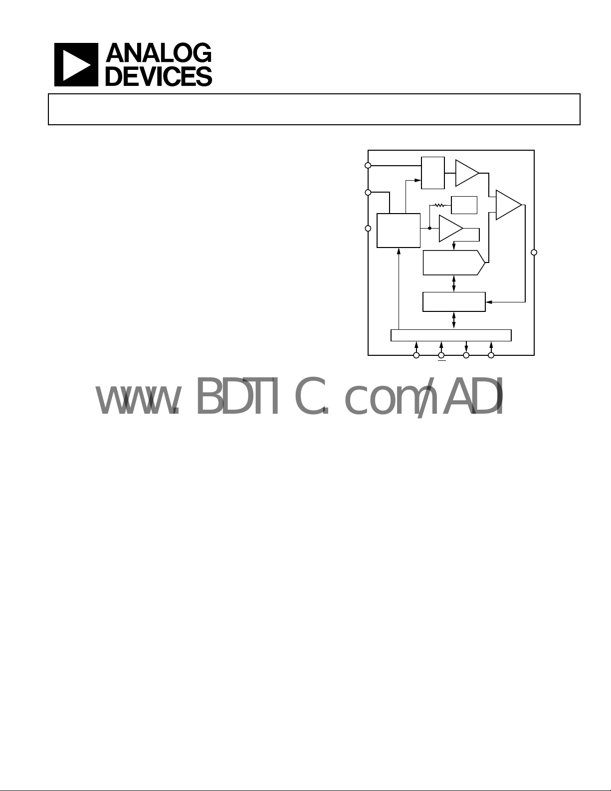
FUNCTIONAL BLOCK DIAGRAM
AIN0
IN1/
V
REF
V
DD
AIN1/V
SOFTWARE
CONTRO L
LATCH
REF
DIN
I/P
MUX
REDISTRIBUTI ON
T/H
2.5V
REF
BUF
CHARGE
DAC
SAR + ADC
CONTRO L LO GIC
SPORT
DOUT
CS
Figure 1.
AD7887
AD7887
COMP
SCLK
GND
6191-001
GENERAL DESCRIPTION
The AD7887 is a high speed, low power, 12-bit analog-to-digital
converter (ADC) that operates from a single 2.7 V to 5.25 V
power supply. The AD7887 is capable of 125 kSPS throughput
rate. The input track-and-hold acquires a signal in 500 ns and
features a single-ended sampling scheme. The output coding for
the AD7887 is straight binary, and the part is capable of
converting full power signals of up to 2.5 MHz.
The AD7887 can be configured for either dual- or single-channel
peration via the on-chip control register. There is a default
o
single-channel mode that allows the AD7887 to be operated as a
read-only ADC. In single-channel operation, there is one
analog input (AIN0) and the AIN1/V
function. This V
pin allows the user access to the part’s
REF
internal 2.5 V reference, or the V
external reference to provide the reference voltage for the part.
This external reference voltage has a range of 2.5 V to V
analog input range on AIN0 is 0 to V
In dual-channel operation, the AIN1/V
function, providing a second analog input channel. In this case,
the reference voltage for the part is provided via the V
pin assumes its V
REF
pin can be overdriven by an
REF
DD
.
REF
pin assumes its AIN1
REF
pin. As
DD
REF
. The
a result, the input voltage range on both the AIN0 and AIN1
inputs is 0 to V
DD
.
CMOS construction ensures low power dissipation of typically
2 mW fo
r normal operation and 3 μW in power-down mode.
The part is available in an 8-lead, 0.15-inch-wide narrow body
SOIC and an 8-lead MSOP package.
PRODUCT HIGHLIGHTS
1. Smallest 12-bit dual-/single-channel ADC; 8-lead MSOP
package.
owest power 12-bit dual-/single-channel ADC.
2. L
lexible power management options, including automatic
3. F
power-down after conversion.
ad-only ADC capability.
4. Re
5. Ana
6. V
log input range from 0 V to V
ersatile serial input/output port (SPI/QSPI/MICROWIRE/
DSP compatible).
REF
.
Rev. C
Information furnished by Analog Devices is believed to be accurate and reliable. However, no
responsibility is assumed by Anal og Devices for its use, nor for any infringements of patents or ot her
rights of third parties that may result from its use. Specifications subject to change without notice. No
license is granted by implication or otherwise under any patent or patent rights of Analog Devices.
Trademarks and registered trademarks are the property of their respective owners.
One Technology Way, P.O. Box 9106, Norwood, MA 02062-9106, U.S.A.
Tel: 781.329.4700 www.analog.com
Fax: 781.461.3113 ©2006 Analog Devices, Inc. All rights reserved.
Page 2

AD7887
www.BDTIC.com/ADI
TABLE OF CONTENTS
Features.............................................................................................. 1
Applications....................................................................................... 1
Functional Block Diagram .............................................................. 1
General Description ......................................................................... 1
Product Highlights ........................................................................... 1
Revision History ............................................................................... 2
Specifications..................................................................................... 3
Timing Specifications .................................................................. 5
Absolute Maximum Ratings............................................................ 6
ESD Caution.................................................................................. 6
Pin Configurations and Function Descriptions ........................... 7
Typical Performance Characteristics ............................................. 8
Terminology ...................................................................................... 9
Control Register.............................................................................. 10
Theory of Operation ...................................................................... 11
Circuit Information.................................................................... 11
Converter Operation.................................................................. 11
ADC Transfer Function............................................................. 11
Typical Connection Diagram ................................................... 11
Analog Input............................................................................... 12
Power-Down Options................................................................ 13
Power vs. Throughput Rate....................................................... 13
Modes of Operation................................................................... 13
Serial Interface............................................................................ 17
Microprocessor Interfacing....................................................... 18
Application Hints ....................................................................... 20
Outline Dimensions....................................................................... 21
Ordering Guide............................................................................... 21
REVISION HISTORY
9/06—Rev. B to Rev. C
Updated Format..................................................................Universal
Change to Absolute Maximum Ratings......................................... 6
Additions to Pin Configurations.................................................... 7
Added Table 7.................................................................................. 18
Updated Outline Dimensions....................................................... 21
Changes to Ordering Guide.......................................................... 21
Rev. C | Page 2 of 24
Page 3

AD7887
www.BDTIC.com/ADI
SPECIFICATIONS
VDD = 2.7 V to 5.25 V, V
Table 1.
Parameter
DYNAMIC PERFORMANCE
Signal to Noise + Distortion Ratio (SNR)2, 371 71 dB typ fIN = 10 kHz sine wave, f
Total Harmonic Distortion (THD)2 −80 −80 dB typ fIN = 10 kHz sine wave, f
Peak Harmonic or Spurious Noise2 –80 −80 dB typ fIN = 10 kHz sine wave, f
Intermodulation Distortion (IMD)2
Second-Order Terms −80 −80 dB typ fa = 9.983 kHz, fb = 10.05 kHz, f
Third-Order Terms −80 −80 dB typ fa = 9.983 kHz, fb = 10.05 kHz, f
Channel-to-Channel Isolation2 −80 −80 dB typ fIN = 25 kHz
Full-Power Bandwidth 2.5 2.5 MHz typ @ 3 dB
DC ACCURACY Any channel
Resolution 12 12 Bits
Integral Nonlinearity2 ±2 ±1 LSB max
Differential Nonlinearity2 ±2 ±1 LSB max Guaranteed no missing codes to 11 bits (A Grade)
Offset Error2 ±3 ±3 LSB max VDD = 5 V, dual-channel mode
±4 ±4 LSB max VDD = 3 V, dual-channel mode
±6 ±6 LSB typ Single-channel mode
Offset Error Match2 0.5 0.5 LSB max
Gain Error2 ±2 ±2 LSB max Dual-channel mode
±1 ±1 LSB max Single-channel mode, external reference
±6 ±6 LSB typ Single-channel mode, internal reference
Gain Error Match2 2 2 LSB max
ANALOG INPUT
Input Voltage Ranges 0 to V
Leakage Current ±5 ±5 μA max
Input Capacitance 20 20 pF typ
REFERENCE INPUT/OUTPUT
REFIN Input Voltage Range 2.5/VDD 2.5/VDD V min/max Functional from 1.2 V
Input Impedance 10 10 kΩ typ Very high impedance if internal reference disabled
REF
Output Voltage 2.45/2.55 2.45/2.55 V min/max
OUT
REF
Temperature Coefficient ±50 ±50 ppm/°C typ
OUT
LOGIC INPUTS
Input High Voltage, V
2.1 2.1 V min VDD = 2.7 V to 3.6 V
Input Low Voltage, V
Input Current, IIN ±1 ±1 μA max Typically 10 nA, VIN = 0 V or VDD
Input Capacitance, C
LOGIC OUTPUTS
Output High Voltage, VOH I
V
Output Low Voltage, VOL 0.4 0.4 V max I
Floating-State Leakage Current ±1 ±1 μA max
Floating-State Output Capacitance5 10 10 pF max
Output Coding Straight (Natural) Binary
= 2.5 V, external/internal reference unless otherwise noted, f
REF
A
V
2.4 2.4 V min VDD = 4.75 V to 5.25 V
INH
0.8 0.8 V max VDD = 2.7 V to 5.25 V
INL
4
IN
10 10 pF max
1
ersion
REF
− 0.5 VDD − 0.5 V min VDD = 2.7 V to 5.25 V
DD
B Version1Unit Test Conditions/Comments
0 to V
V
REF
= 2 MHz, TA = T
SCLK
SOURCE
= 200 μA
SINK
MIN
= 200 μA
to T
, unless otherwise noted.
MAX
= 125 kSPS
SAMPLE
= 125 kSPS
SAMPLE
= 125 kSPS
SAMPLE
SAMPLE
SAMPLE
= 125 kSPS
= 125 kSPS
Rev. C | Page 3 of 24
Page 4

AD7887
www.BDTIC.com/ADI
A
Parameter
Version
CONVERSION RATE
Throughput Time 16 16 SCLK cycles
Track/Hold Acquisition Time2 1.5 1.5 SCLK cycles
Conversion Time 14.5 14.5 SCLK cycles 7.25 μs (2 MHz Clock)
POWER REQUIREMENTS
VDD +2.7/+5.25 +2.7/+5.25 V min/max
IDD
Normal Mode5 (Mode 2)
Static 700 700 μA max
Operational (f
= 125 kSPS) 850 850 μA typ Internal reference enabled
SAMPLE
700 700 μA typ Internal reference disabled
Using Standby Mode (Mode 4) 450 450 μA typ f
Using Shutdown Mode (Modes 1, 3) 120 120 μA typ f
12 12 μA typ f
Standby Mode6 210 210 μA max VDD = 2.7 V to 5.25 V
Shutdown Mode6 1 1 μA max VDD = 2.7 V to 3.6 V
2 2 μA max VDD = 4.75 V to 5.25 V
Normal Mode Power Dissipation 3.5 3.5 mW max VDD = 5 V
2.1 2.1 mW max VDD = 3 V
Shutdown Power Dissipation 5 5 μW max VDD = 5 V
3 3 μW max VDD = 3 V
Standby Power Dissipation 1.05 1.05 mW max VDD = 5 V
630 630 μW max VDD = 3 V
1
Temperature range for A and B versions is −40°C to +125°C.
2
See the Terminology section.
3
SNR calculation includes distortion and noise components.
4
Sample tested at +25°C to ensure compliance.
5
All digital inputs at GND except CS at VDD. No load on the digital outputs. Analog inputs at GND.
6
SCLK at GND when SCLK off. All digital inputs at GND except for CS at VDD. No load on the digital outputs. Analog inputs at GND.
1
B Version1Unit Test Conditions/Comments
Conversion time plus acquisition time is 125 kSPS,
with 2 MH
SAMPLE
SAMPLE
SAMPLE
z Clock
= 50 kSPS
= 10 kSPS
= 1 kSPS
Rev. C | Page 4 of 24
Page 5
AD7887
O
www.BDTIC.com/ADI
TIMING SPECIFICATIONS
1
Table 2.
Limit at T
MIN
, T
MAX
(A, B Versions)
Parameter 4.75 V to 5.25 V 2.7 V to 3.6 V Unit Description
2
f
2 2 MHz max
SCLK
t
14.5 × t
CONVER T
t
1.5 × t
ACQ
14.5 × t
SCLK
1.5 × t
SCLK
SCLK
SCLK
t1 10 10 ns min
3
t
2
3
t
3
30 60 ns max
75 100 ns max Data access time after SCLK falling edge
Throughput time = t
to SCLK setup time
CS
Delay from CS
until DOUT three-state disabled
CONVER T
+ t
ACQ
= 16 t
SCLK
t4 20 20 ns min Data setup time prior to SCLK rising edge
t5 20 20 ns min Data valid to SCLK hold time
t6 0.4 × t
t7 0.4 × t
4
t
8
80 80 ns max
0.4 × t
SCLK
0.4 × t
SCLK
ns min SCLK high pulse width
SCLK
ns min SCLK low pulse width
SCLK
rising edge to DOUT high impedance
CS
t9 5 5 μs typ Power-up time from shutdown
1
Sample tested at 25°C to ensure compliance. All input signals are specified with tr = tf = 5 ns (10% to 90% of VDD) and timed from a voltage level of 1.6 V.
2
Mark/space ratio for the SCLK input is 40/60 to 60/40.
3
Measured with the load circuit of Figure 2 and defined as the time required for the output to cross 0.8 V or 2.0 V.
4
t8 is derived from the measured time taken by the data outputs to change 0.5 V when loaded with the circuit of Figure 2. The measured number is then extrapolated
back to remove the effects of charging or discharging the 50 pF capacitor. This means that the time, t8, quoted in the timing characteristics is the true bus relinquish
time of the part and is independent of the bus loading.
200µA I
TO
UTPUT
PIN
C
L
50pF
200µA I
Figure 2. Load Circuit for Digital Out
OL
1.6V
OH
06191-002
put Timing Specifications
Rev. C | Page 5 of 24
Page 6
AD7887
www.BDTIC.com/ADI
ABSOLUTE MAXIMUM RATINGS
TA = 25°C, unless otherwise noted.
Table 3.
Parameter Rating
VDD to AGND −0.3 V to +7 V
Analog Input Voltage to AGND −0.3 V to VDD + 0.3 V
Digital Input Voltage to AGND −0.3 V to VDD + 0.3 V
Digital Output Voltage to AGND −0.3 V to VDD + 0.3 V
REFIN/REF
Input Current to Any Pin Except Supplies1 ±10 mA
Operating Temperature Range
Commercial Temperature Range
Storage Temperature Range −65°C to +150°C
Junction Temperature +150°C
SOIC or MSOP Package Power Dissipation 450 mW
θJA Thermal Impedance 157°C/W (SOIC)
205.9°C/W (MSOP)
θJC Thermal Impedance 56°C/W (SOIC)
43.74°C/W (MSOP)
Lead Temperature, Soldering
Pb-Free Temperature, Soldering Reflow 260(0)°C
ESD 4 kV
1
Transient currents of up to 100 mA do not cause SCR latch-up.
to AGND −0.3 V to VDD + 0.3 V
OUT
A, B Versions −40°C to +125°C
Vapor Phase (60 sec) 215°C
Infrared (15 sec) 220°C
Stresses above those listed under Absolute Maximum Ratings
may cause permanent damage to the device. This is a stress
rating only; functional operation of the device at these or any
other conditions above those indicated in the operational
section of this specification is not implied. Exposure to absolute
maximum rating conditions for extended periods may affect
device reliability.
ESD CAUTION
Rev. C | Page 6 of 24
Page 7
AD7887
www.BDTIC.com/ADI
PIN CONFIGURATIONS AND FUNCTION DESCRIPTIONS
1
CS
AD7887
2
V
DD
GND
3
TOP VIEW
(Not to Scale)
REF
4
AIN1/V
Figure 3. SOIC_N Pin Configuration Figure 4. MSOP Pin Configuration
Table 4. Pin Function Descriptions
Pin No. Mnemonic Description
1
Chip Select. Active low logic input. This input provides the dual function of initiating conversions on the AD7887
CS
and also frames the serial data transfer. When the AD7887 operates in its default mode, the CS
the shutdown pin such that with the CS
2 VDD
Power Supply Input. The V
two-channel operation, this pin also provides the reference source for the part.
3 GND
Ground Pin. This pin is the ground reference point for all cir
and DGND planes, these planes should be tied together as close as possible to this GND pin. Where this is not
possible, this GND pin should connect to the AGND plane.
4 AIN1/V
REF
Analog Input 1/Voltage Reference Input. In single-channel mod
In this case, the user can either access the internal 2.5 V reference or overdrive the internal reference with the
voltage applied to this pin. The reference voltage range for an externally applied reference is 1.2 V to V
channel mode, this pin provides the second analog input channel, AIN1. The input voltage range on AIN1 is
0 to V
.
DD
5 AIN0
Analog Input 0. In single-channel mode, this is the analog input and the input v
channel mode, it has an analog input range of 0 to V
6 DIN
Data In. Logic Input. Data to be written to the AD7887’s contr
the register on the rising edge of SCLK (see the Control Register section). The AD7887 can be operated as a
-channel, read-only ADC by tying the DIN line permanently to GND.
single
7 DOUT
Data Out. Logic output. The conversion result from the AD7887 is provided on this output as a ser
The bits are clocked out on the falling edge of the SCLK input. The data stream consists of four leading zeros
followed by the 12 bits of conversion data, which is provided MSB first.
8 SCLK
Serial Clock. Logic input. SCLK provides the serial clock for ac
the control register. This clock input is also used as the clock source for the AD7887’s conversion process.
8
7
6
5
SCLK
DOUT
DIN
AIN0
1
CS
AD7887
2
V
DD
GND
AIN1/V
06191-003
REF
TOP VIEW
3
(Not to Scale)
4
pin high, the AD7887 is in its power-down mode.
range for the AD7887 is from 2.7 V to 5.25 V. When the AD7887 is configured for
DD
cuitry on the AD7887. In systems with separate AGND
e, this pin becomes the reference input/output.
.
DD
ol register is provided on this input and clocked into
cessing data from the part and writing serial data to
8
SCLK
DOUT
7
DIN
6
AIN0
5
06191-004
pin also acts as
oltage range is 0 to V
ial data stream.
. In two-
DD
. In dual-
REF
Rev. C | Page 7 of 24
Page 8
AD7887
R
–
www.BDTIC.com/ADI
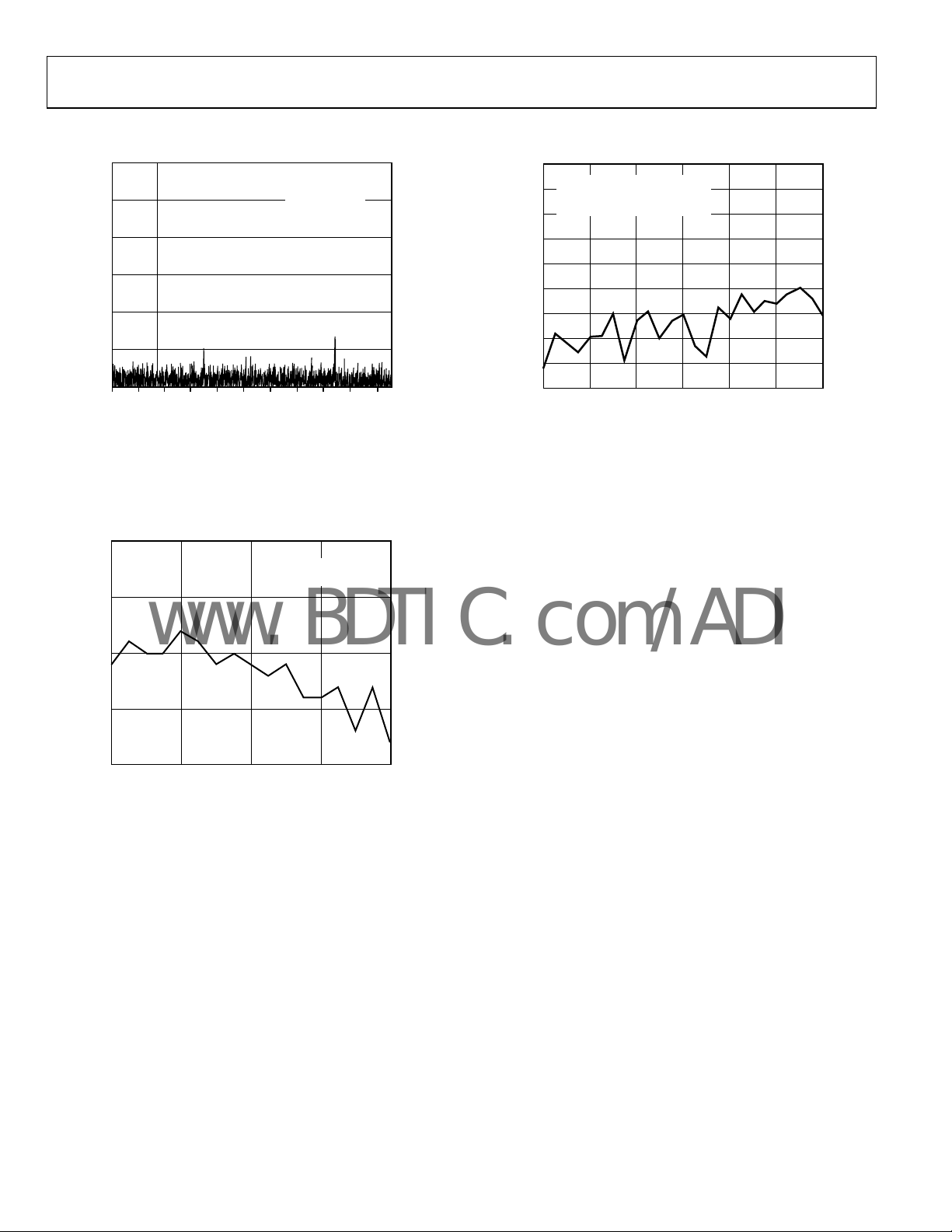
TYPICAL PERFORMANCE CHARACTERISTICS
–10
–30
–50
–70
–90
–110
0
4096 POINT FFT
SAMPLING
125kSPS
f
= 10kHz
IN
SNR = 71dB
6.103516012.20703
18.31055
24.41406
30.51758
36.62109
42.72461
48.82813
54.93164
61.03516
06191-005
Figure 5. Dynamic Performance
75
VDD = 5.5V/2. 7V
–77
100mV p-p SI NE WAVE O N V
REFIN = 2.488V EXT REFERENCE
–79
–81
–83
–85
PSRR (dB)
–87
–89
–91
–93
2.65
12.85
Figure 7. PSRR vs. Frequency
DD
23.15 33.65
INPUT FREQ UENCY (kHz)
43.85 54.35
64.15
06191-007
73.0
VDD = 5V
5V EXT REFERENCE
72.5
(dB)
72.0
SN
71.5
71.0
0.15 42.14
21.14
INPUT FREQ UENCY (kHz)
31.5910.89
6191-006
Figure 6. SNR vs. Input Frequency
Rev. C | Page 8 of 24
Page 9

AD7887
www.BDTIC.com/ADI
TERMINOLOGY
Integral Nonlinearity
This is the maximum deviation from a straight line passing
rough the endpoints of the ADC transfer function. The end-
th
points of the transfer function are zero scale, a point ½ LSB
below the first code transition, and full scale, a point ½ LSB
above the last code transition.
Differential Nonlinearity
This is the difference between the measured and the ideal 1 LSB
ch
ange between any two adjacent codes in the ADC.
Offset Error
This is the deviation of the first code transition (00 . . . 000) to
(00 . . . 001) f
rom the ideal, that is, AGND + 0.5 LSB.
Offset Error Match
This is the difference in offset error between any two channels.
Gain Error
This is the deviation of the last code transition (111 . . . 110) to
(111 . . . 111) f
rom the ideal (that is, V
− 1.5 LSB) after the
REF
offset error has been adjusted out.
Gain Error Match
This is the difference in gain error between any two channels.
Trac k / Hold Ac q u isiti o n Ti me
The track/hold amplifier returns to track mode at the end of
co
nversion. Track/hold acquisition time is the time required for
the output of the track/hold amplifier to reach its final value,
within ±1/2 LSB, after the end of a conversion.
Signal to (Noise + Distortion) Ratio
This is the measured ratio of signal to (noise + distortion) at the
o
utput of the ADC. The signal is the rms amplitude of the fundamental. Noise is the sum of all nonfundamental signals up to half
the sampling frequency (f
/2), excluding dc. The ratio is dependent
S
on the number of quantization levels in the digitization process: the
more levels, the smaller the quantization noise. The theoretical
signal to (noise + distortion) ratio for an ideal N-bit converter
with a sine wave input is given by
Signal to (Noise + Distortion) = (6.02
N + 1.76) dB
Thus for a 12-bit converter, this is 74 dB.
Total Harmonic Distortion
Total harmonic distortion (THD) is the ratio of the rms sum of
rmonics to the fundamental. For the AD7887, it is defined as
ha
2
2
2
2
2
2
THD
where V
V
is the rms amplitude of the fundamental and V2, V3,
1
, V5, and V6 are the rms amplitudes of the second through the
4
log20)dB(
=
4
3
V
1
VVVVV
++++
5
6
sixth harmonics.
Peak Harmonic or Spurious Noise
Peak harmonic or spurious noise is defined as the ratio of the
rms value of the next largest component in the ADC output
spectrum (up to f
/2 and excluding dc) to the rms value of the
S
fundamental. Normally, the value of this specification is
determined by the largest harmonic in the spectrum, but for
ADCs where the harmonics are buried in the noise floor, the
largest harmonic could be a noise peak.
Intermodulation Distortion
With inputs consisting of sine waves at two frequencies, fa and fb,
any active device with nonlinearities creates distortion products
at sum and difference frequencies of mfa ± nfb where m, n = 0,
1, 2, 3, and so on. Intermodulation distortion terms are those for
which neither m nor n are equal to 0. For example, the secondorder terms include (fa + fb) and (fa − fb), and the third order
terms include (2fa + fb), (2fa − fb), (fa + 2fb) and (fa − 2fb).
The AD7887 is tested using the CCIF standard in which two
in
put frequencies near the top end of the input bandwidth are
used. In this case, the second-order terms are usually distanced
in frequency from the original sine waves, and the third-order
terms are usually at a frequency close to the input frequencies.
As a result, the second- and third-order terms are specified
separately. The calculation of the intermodulation distortion is
as per the THD specification, where it is the ratio of the rms
sum of the individual distortion products to the rms amplitude
of the sum of the fundamentals expressed in decibels.
Channel-to-Channel Isolation
Channel-to-channel isolation is a measure of the level of
crosstalk between channels. It is measured by applying a fullscale 25 kHz sine wave signal to the nonselected input channel
and determining how much that signal is attenuated in the
selected channel. The figure given is the worst case across both
channels for the AD7887.
Power Supply Rejection (PSR)
Variations in power supply affect the full-scale transition, but
not the converter’s linearity. PSR is the maximum change in the
full-scale transition point due to a change in power supply voltage
from the nominal value. See
Figure 7.
PSRR is defined as the ratio of the power in the ADC output at
f
requency f to the power of a full-scale sine wave applied to the
ADC of frequency f
:
S
PSRR (dB) = 10 log(Pf/Pfs)
where Pf is th
the power at frequency f
e power at frequency f in ADC output and Pfs is
in ADC full-scale input.
S
Rev. C | Page 9 of 24
Page 10

AD7887
www.BDTIC.com/ADI
CONTROL REGISTER
The control register on the AD7887 is an 8-bit, write-only register. Data is loaded from the DIN pin of the AD7887 on the rising edge of
SCLK. The data is transferred on the DIN line at the same time as the conversion result is read from the part. This requires 16 serial
CS
clocks for every data transfer. Only the information provided on the first eight rising clock edges after
control register. MSB denotes the first bit in the data stream. The bit functions are outlined in Tab le 5 . The contents of the control register
power up is all 0s.
on
MSB
DONTC ZERO REF SIN/DUAL CH ZERO PM1 PM0
Table 5. Control Register
Bit Mnemonic Comment
7 DONTC
6 ZERO A zero must be written to this bit to ensure correct operation of the AD7887.
5 REF
4 SIN/DUAL
3 CH
2 ZERO A 0 must be written to this bit to ensure correct operation of the AD7887.
1, 0 PM1, PM0 Power Management Bits. These two bits decode the mode of operation of the AD7887 as described in Table 6.
Don’t Care. The value written to this bit of the control register is
is 0 or 1.
Reference Bit. With a 0 in this bit, the on-chip reference is enabled
disabled.
Single/Dual Bit. This bit determines whether the AD7887 oper
0 in this bit selects single-channel operation and the AIN1/V
dual-channel mode, with the reference voltage for the ADC internally connected to V
assuming its AIN1 function as the second analog input channel. To obtain best performance from the AD7887,
the internal reference should be disabled when operating in the dual-channel mode, that is, REF = 1.
Channel Bit. When the part is selected for dual-channel mode, this bit determines which channel is converted
or the next conversion. A 0 in this bit selects the AIN0 input, and a 1 in this bit selects the AIN1 input. In single-
f
channel mode, this bit should always be 0.
a don’t care, that is, it doesn’t matter if the bit
. With a 1 in this bit, the on-chip reference is
ates in single-channel or dual-channel mode. A
pin assumes its V
REF
falling edge is loaded to the
function. A 1 in this bit selects
REF
and the AIN1/V
DD
REF
pin
Table 6. Power Management Options
PM1 PM0 Mode
0 0
0 1 Mode 2. In this mode, the AD7887 is always fully powered up, regardless of the status of any of the logic inputs.
1 0
1 1
Mode 1. In this mode, the AD7887 en
Thus the part comes out of shutdown on the falling edge of CS and enters shutdown on the rising edge of CS.
Mode 3. In this mode, the AD7887 automatically enters shutdo
regardless of the state of CS
Mode 4. In this standby mode, portions of the AD7887 are powered down but the on-chip reference voltage
emains powered up. This mode is similar to Mode 3, but allows the part to power up much faster. The REF bit
r
should be 0 to ensure that the on-chip reference is enabled.
.
ters shutdown if the CS
input is 1 and is in full power mode when CS is 0.
wn mode at the end of each conversion,
Rev. C | Page 10 of 24
Page 11

AD7887
A
V
www.BDTIC.com/ADI
THEORY OF OPERATION
CIRCUIT INFORMATION
The AD7887 is a fast, low power, 12-bit, single-supply, singlechannel/dual-channel ADC. The part can be operated from a
3 V (2.7 V to 3.6 V) supply or from a 5 V (4.75 V to 5.25 V) supply.
When operated from either a 5 V or 3 V supply, the AD7887 is
capable of throughput rates of 125 kSPS when provided with a
2 MHz clock.
The AD7887 provides the user with an on-chip, track/hold
nalog-to-digital converter reference and a serial interface
a
housed in an 8-lead package. The serial clock input accesses data
from the part and provides the clock source for the successive
approximation ADC. The part can be configured for singlechannel or dual-channel operation. When configured as a
single-channel part, the analog input range is 0 to V
externally applied V
can be between 1.2 V and VDD). When
REF
(where the
REF
the AD7887 is configured for two input channels, the input
range is determined by internal connections to be 0 to V
DD
.
If single-channel operation is required, the AD7887 can be
o
perated in a read-only mode by tying the DIN line permanently
to GND. For applications where the user wants to change the
mode of operation or wants to operate the AD7887 as a dualchannel ADC, the DIN line can be used to clock data into the
part’s control register.
CONVERTER OPERATION
The AD7887 is a successive approximation ADC built around a
charge-redistribution DAC. Figure 8 and Figure 9 show simplified
hematics of the ADC.
sc
acq
uisition phase. SW2 is closed and SW1 is in Position A, the
comparator is held in a balanced condition, and the sampling
capacitor acquires the signal on AIN.
SAMPLING
CAPACITOR
A
IN
SW1
B
AGND
ACQUISITION
(REF IN/REF OUT)/2
When the ADC starts a conversion (see Figure 9), SW2 opens
and SW1 moves to Position B, causing the comparator to become
unbalanced. The control logic and the charge-redistribution DAC
are used to add and subtract fixed amounts of charge from the
sampling capacitor to bring the comparator back into a balanced
condition. When the comparator is rebalanced, the conversion
is complete. The control logic generates the ADC output code.
Figure 10 shows the ADC transfer function.
Figure 8 shows the ADC during its
SW2
PHASE
Figure 8. ADC Acquisition Phase
COMPARAT OR
CHARGE
REDISTRIBUT ION
DAC
CONTROL
LOGIC
Rev. C | Page 11 of 24
SAMPLING
CAPACITOR
A
IN
SW1
B
CONVERSION
AGND
(REF IN/REF OUT)/2
PHASE
SW2
COMPARAT OR
Figure 9. ADC Conversion Phase
ADC TRANSFER FUNCTION
The output coding of the AD7887 is straight binary. The
designed code transitions occur at successive integer LSB values
(that is, 1 LSB, 2 LSB, and so on). The LSB size is V
ideal transfer characteristic for the AD7887 is shown in
10.
111 ... 111
111 ... 110
111 ... 000
ADC CODE
011 ... 111
000 ... 010
000 ... 001
000 ... 000
0.5LSB
0V
Figure 10. Transfer Characteristic
1LSB = V
ANALOG INP UT
REF
TYPICAL CONNECTION DIAGRAM
Figure 11 shows a typical connection diagram for the AD7887.
The GND pin is connected to the analog ground plane of the
system. The part is in dual-channel mode so V
connected to a well-decoupled V
input range of 0 V to V
. The conversion result is output in a
DD
16-bit word with four leading zeros followed by the MSB of the
12-bit result. For applications where power consumption is of
concern, the automatic power-down at the end of conversion
should be used to improve power performance. See the
0V TO V
INPUT
section.
10µF
0.1µF
DD
Figure 11. Typical Connection Diagram
AIN1
AIN2
GND
Operation
06191-008
of
SUPPLY 2.7V
TO 5.25V
pin to provide an analog
DD
SERIAL
V
DD
INTERFACE
AD7887
SCLK
DOUT
DIN
CS
CHARGE
REDISTRIBUT ION
CONTROL
REF
/4096
– 1.5LSB
+V
REF
is internally
REF
DAC
LOGIC
/4096. The
Figure
06191-010
Modes
µC/µP
06191-009
06191-011
Page 12

AD7887
V
–
www.BDTIC.com/ADI
ANALOG INPUT
Figure 12 shows an equivalent circuit of the analog input
structure of the AD7887. The two diodes, D1 and D2, provide
ESD protection for the analog inputs. Care must be taken to
ensure that the analog input signal never exceed the supply rails
by more than 200 mV. Exceeding this value causes the diodes
to become forward biased and to start conducting into the
substrate. The maximum current these diodes can conduct
without causing irreversible damage to the part is 20 mA.
However, it is worth noting that a small amount of current
(1 mA) being conducted into the substrate due to an
overvoltage on an unselected channel can cause inaccurate
C2
Figure 12 is
06191-012
conversions on a selected channel. Capacitor C1 in
t
ypically about 4 pF and can primarily be attributed to pin
capacitance. Resistor R1 is a lumped component made up of the
on resistance of a multiplexer and a switch. This resistor is
typically about 100 Ω. Capacitor C2 is the ADC sampling
capacitor and typically has a capacitance of 20 pF.
Note that the analog input capacitance seen when in track mode
ically 38 pF, whereas in hold mode it is typically 4 pF.
is typ
DD
D1
V
IN
C1
D2
4pF
Figure 12. Equivalent Analog Input Circuit
CONVERSION PHASE —SWITCH O PEN
TRACK PHASE—SWI TCH CLOSED
20pF
R1
For ac applications, removing high frequency components from
the analog input signal is recommended by use of an RC
low-pass filter on the relevant analog input pin. In applications
where harmonic distortion and signal-to-noise ratio are critical,
the analog input should be driven from a low impedance
source. Large source impedances will significantly affect the ac
performance of the ADC. This may necessitate the use of an
input buffer amplifier. The choice of op amp is a function of the
particular application.
When no amplifier is used to drive the analog input, the source
pedance should be limited to low values. The maximum
im
source impedance depends on the amount of total harmonic
distortion (THD) that can be tolerated. The THD increases as
the source impedance increases and performance degrades.
Figure 13 shows a graph of the total harmonic distortion vs. the
a
nalog input signal frequency for different source impedances.
65
THD vs. FREQUENCY FOR DIFFERENT
SOURCE IMPEDANCES
VDD = 5V
–70
5V EXT REFERENCE
–75
THD (dB)
–80
–85
–90
RIN = 10Ω, CIN = 10nF
10.89 31.5921.14
INPUT FREQ UENCY (kHz)
Figure 13. THD vs. Analog Input Frequency
RIN = 1kΩ, CIN = 100pF
RIN = 50Ω, CIN = 2.2nF
41.2451.0
49.86
6191-013
On-Chip Reference
The AD7887 has an on-chip 2.5 V reference. This reference can
be enabled or disabled by clearing or setting the REF bit in the
control register, respectively. If the on-chip reference is to be used
externally in a system, it must be buffered before it is applied
elsewhere. If an external reference is applied to the device, the
internal reference is automatically overdriven. However, it is
advised to disable the internal reference by setting the REF bit
in the control register when an external reference is applied in
order to obtain optimum performance from the device. When
the internal reference is disabled, SW1, shown in
pens and the input impedance seen at the AIN1/V
o
Figure 14,
pin is the
REF
input impedance of the reference buffer, which is in the region
of gigaohms. When the internal reference is enabled, the input
impedance seen at the pin is typically 10 kΩ. When the AD7887
is operated in two-channel mode, the reference is taken from
internally, not from the on-chip 2.5 V reference.
V
DD
AIN1/V
REF
SW1
10kΩ
2.5V
Figure 14. On-Chip R
eference Circuitry
06191-014
Rev. C | Page 12 of 24
Page 13

AD7887
www.BDTIC.com/ADI
po
POWER-DOWN OPTIONS
The AD7887 provides flexible power management to allow
the user to achieve the best power performance for a given
throughput rate.
The power management options are selected by programming
t
he power management bits (that is, PM1 and PM0) in the
control register.
hen the power management bits are programmed for either
W
Tabl e 6 summarizes the available options.
of the auto power-down modes, the part enters power-down
th
mode on the 16
The first falling SCLK edge after the
rising SCLK edge after the falling edge of CS.
CS
falling edge causes the
part to power up again. When the AD7887 is in Mode 1, that is,
PM1 = PM0 = 0, the part enters shutdown on the rising edge of
CS
and power up from shutdown on the falling edge of CS. If
CS
is brought high during the conversion in this mode, the part
immediately enters shutdown.
Power-Up Times
The AD7887 has an approximate 1 μs power-up time when
powering up from standby or when using an external reference.
When V
is first connected the AD7887 powers up in Mode 1,
DD
that is, PM1 = PM0 = 0. The part is put into shutdown on the
CS
rising edge of
in this mode. A subsequent power-up from
shutdown takes approximately 5 μs. The AD7887 wake-up time
is very short in the autostandby mode; therefore, it is possible to
wake up the part and carry out a valid conversion in the same
read/write operation.
POWER VS. THROUGHPUT RATE
By operating the AD7887 in autoshutdown mode, autostandby
mode, or Mode 1, the average power consumption of the
AD7887 decreases at lower throughput rates.
h
ow as the throughput rate is reduced, the device remains in its
power-down state longer and the average power consumption
over time drops accordingly.
For example, if the AD7887 is operated in a continuous sampling
ode with a throughput rate of 10 kSPS and a SCLK of 2 MHz
m
= 5 V), PM1 = 1 and PM0 = 0, that is, the device is in auto-
(V
DD
shutdown mode, and the on-chip reference is used, the power
consumption is calculated as follows: The power dissipation
during normal operation is 3.5 mW (V
DD
time is 5 μs and the remaining conversion plus acquisition time
is 15.5 t
, that is, approximately 7.75 μs (see Figure 18), the
SCLK
AD7887 can be said to dissipate 3.5 mW for 12.75 μs during
each conversion cycle. If the throughput rate is 10 kSPS, the
cycle time is 100 μs and the average power dissipated during
each cycle is (12.75/100) × (3.5 mW) = 446.25 μW. If V
SCLK = 2 MHz, and the device is in autoshutdown mode using the
on-chip reference, the power dissipation during normal operation
is 2.1 mW. The AD7887 can now be said to dissipate 2.1 mW
for 12.75 μs during each conversion cycle. With a throughput
rate of 10 kSPS, the average power dissipated during each cycle
is (12.75/100) × (2.1 mW) = 267.75 μW.
Figure 15 shows
= 5 V). If the power-up
= 3 V,
DD
Figure 15 shows the
Rev. C | Page 13 of 24
wer vs. throughput rate for automatic shutdown with both
5 V and 3 V supplies.
10
VDD = 5V
SCLK = 2MHz
VDD = 3V
SCLK = 2MHz
10
Figure 15. Power vs. Throughput Rate
20 504030
THROUGHPUT RAT E (kSPS)
06191-015
POWER (mW)
0.01
1
0.1
0
MODES OF OPERATION
The AD7887 has several modes of operation that are designed
to provide flexible power management options. These options
can be chosen to optimize the power dissipation/throughput
rate ratio for differing application requirements. The modes of
operation are controlled by the PM1 and PM0 bits of the control
register, as previously outlined in
f the AD7887, the default mode of all 0s in the control register
o
can be set up by tying the DIN line permanently low.
Mode 1 (PM1 = 0, PM0 = 0)
This mode allows the user to control the powering down of the
part via the
powered up; whenever
shutdown. When
CS
pin. Whenever CS is low, the AD7887 is fully
CS
CS
goes from high to low, all on-chip circuitry
starts to power up. It takes approximately 5 μs for the AD7887
internal circuitry to be fully powered up. As a result, a
conversion (or sample-and-hold acquisition) should not be
initiated during this 5 μs.
Figure 16 shows a general diagram of the operation of the
AD7887 in this
mode. The input signal is sampled on the
second rising edge of SCLK following the
user should ensure that 5 μs elapses between the falling edge of
CS
and the second rising edge of SCLK. In microcontroller
applications, this is readily achievable by driving the
from one of the port lines and ensuring that the serial data read
(from the microcontrollers serial port) is not initiated for 5 μs.
In DSP applications, where
serial frame synchronization line, it is usually not possible to
separate the
CS
falling edge and second SCLK rising edge by up
to 5 μs without affecting the speed of the rest of the serial clock.
Therefore, the user must write to the control register to exit this
mode and (by writing PM1 = 0 and PM0 = 1) put the part into
Mode 2, that is, normal mode. A second conversion needs to be
initiated when the part is powered up to get a conversion result.
The write operation that takes place in conjunction with this
Tabl e 6. For read-only operation
is high, the AD7887 is in full
CS
falling edge. The
CS
CS
is generally derived from the
input
Page 14

AD7887
www.BDTIC.com/ADI
second conversion can put the part back into Mode 1, and the
part goes into power-down mode when
CS
returns high.
Mode 2 (PM1 = 0, PM0 = 1)
In this mode of operation, the AD7887 remains fully powered
CS
low again.
CS
line. It is intended for fastest
up regardless of the status of the
throughput rate performance because the user does not have to
worry about the 5 μs power-up time previously mentioned.
Figure 17 shows the general diagram of the operation of the
AD7887 in this
The data presented to the AD7887 on the DIN line during the
f
irst eight clock cycles of the data transfer are loaded to the
control register. To continue to operate in this mode, the user
must ensure that PM1 is loaded with 0 and PM0 is loaded with
1 on every data transfer.
The falling edge of
signal is sampled on the second rising edge of the SCLK input.
Sixteen serial clock cycles are required to complete the conversion
and access the conversion result. Once a data transfer is complete
(that is, once
immediately by bringing
mode.
CS
initiates the sequence, and the input
CS
returns high), another conversion can be initiated
Mode 3 (PM1 = 1, PM0 = 0)
In this mode, the AD7887 automatically enters its full shutdown
mode at the end of every conversion. It is similar to Mode 1
CS
except that the status of
power-down status of the AD7887.
Figure 18 shows the general diagram of the operation of the
AD7887 in this
goes low, all on-chip circuitry starts to power up. It takes
approximately 5 μs for the AD7887 internal circuitry to be fully
powered up. As a result, a conversion (or sample-and-hold
acquisition) should not be initiated during this 5 μs. The input
signal is sampled on the second rising edge of SCLK following
CS
falling edge. The user should ensure that 5 μs elapses
the
mode. On the first falling SCLK edge after
does not have any effect on the
CS
between the first falling edge of
edge of SCLK after the
In microcontroller applications (or with a slow serial clock), this
is readily achievable by driving the
port lines and ensuring that the serial data read (from the
microcontroller’s serial port) is not initiated for 5 μs. However,
for higher speed serial clocks, it will not be possible to have a
5 μs delay between powering up and the first rising edge of the
SCLK. Therefore, the user must write to the control register to
exit this mode and (by writing PM1 = 0 and PM0 = 1) put the
part into Mode 2. A second conversion needs to be initiated
when the part is powered up to get a conversion result, as
shown in
co
into Mode 3, and the part goes into power-down mode when
the conversion sequence ends.
Figure 19. The write operation that takes place in
njunction with this second conversion can put the part back
CS
Mode 4 (PM1 = 1, PM0 = 1)
In this mode, the AD7887 automatically enters a standby (or
sleep) mode at the end of every conversion. In this standby
mode, all on-chip circuitry, apart from the on-chip reference, is
powered down. This mode is similar to Mode 3, but, in this
case, the power-up time is much shorter because the on-chip
reference remains powered up at all times.
Figure 20 shows the general diagram of the operation of the
AD7887 in this
goes low, the AD7887 comes out of standby. The AD7887 wakeup time is very short in this mode, so it is possible to wake up
the part and carry out a valid conversion in the same read/write
operation. The input signal is sampled on the second rising
edge of SCLK following the
conversion (last rising edge of SCLK), the part automatically
enters its standby mode.
mode. On the first falling SCLK edge after
SCLK
and the second rising
falling edge, as shown in Figure 18.
CS
input from one of the
CS
CS
falling edge. At the end of
Rev. C | Page 14 of 24
Page 15

AD7887
www.BDTIC.com/ADI
DOUT
THE PART POW ERS UP ON CS
FALLING EDGE AS PM1 AND PM0 = 0
CS
1
SCLK
FOUR LEADING ZEROS + CO NVERSION RESUL T
DIN
CONTROL REG ISTER DATA I S LOADED ON THE FIRST EIGHT CLOCKS.
PM1 AND PM0 = 0 TO KEEP THE PART I N THIS MO DE
DATA IN
THE PART POWERS DOWN ON CS
RISING EDGE AS PM1 AND PM0 = 0
16
6191-016
Figure 16. Mode 1 Operation
THE PART REMAI NS POWERED UP
AT ALL TI MES AS
CS
SCLK
DOUT
DIN
1
FOUR LEADING ZEROS + CO NVERSION RES ULT
CONTROL REGISTER DAT A IS LOADED O N THE FIRST EIGHT CLOCKS.
PM1 = 0 AND PM0 = 1 T O KEEP THE PART IN T HIS MODE
PM1 = 0 AND PM0 = 1
DATA IN
Figure 17. Mode 2 Operation
16
6191-017
Rev. C | Page 15 of 24
Page 16

AD7887
www.BDTIC.com/ADI
CS
1
SCLK
DOUT
DIN
FOUR LEADI NG ZEROS + CONVERSIO N RESULT
DATA IN
CONTROL REGISTER DAT A IS LOADED ON THE
FIRST EIGHT CL OCKS. PM1 = 1 AND PM0 = 0
THE PART ENTERS
SHUTDOWN AT THE END OF
CONVERSION AS PM1 = 1 AND PM0 = 0
THE PART PO WERS UP FRO M
SHUTDOWN ON SCLK FALLING EDGE AS
PM1 = 1 AND PM0 = 0
16
1162
t
= 5µs
10
FOUR LEADING ZEROS + CONVERSIO N RESULT
DATA IN
PM1 = 1 AND PM0 = 0 TO KEEP THE
PART IN THIS MODE
6191-018
Figure 18. Mode 3 Operation (Microcontroller for Slow SCLKs)
CS
SCLK
DOUT
THE PART ENTERS
SHUTDOWN AT T HE END
OF CONV ERSIO N AS
PM1 = 1 AND PM0 = 0
1
FOUR LEADING ZEROS
+ CONVERSION RESULT
THE PART BEGI NS TO PO WER
UP FROM SHUTDOW N
168
1
THE PART REMAI NS POWERED UP
AS PM1 = 0 AND PM0 = 1
FOUR LEADING ZEROS
+ CONVERSIO N RESULT
168
1
THE PART ENTERS
SHUTDOWN AT THE END OF
CONVERSION AS PM1 = 1
AND PM0 = 0
8
FOUR LEADING ZEROS
+ CONVERSION RESULT
16
DIN
CONTROL REGISTER DAT A IS LOADED O N
THE FIRST EIGHT CLOCKS. PM1 = 1 AND PM0 = 0
DATA IN
DATA IN
PM1 = 0 AND PM0 = 1 T O PLACE
THE PART IN NO RMAL MODE
DATA IN
PM1 = 1 AND PM0 = 0 T O PLACE
THE PART BACK IN MO DE 3
6191-019
Figure 19. Mode 3 Operation (Microcontroller for High Speed SCLKs)
THE PART POWERS UP
FROM STANDBY O N SCLK
FALLING EDGE AS PM1 = 1
AND PM0 = 1
1
FOUR LEADING ZEROS + CO NVERSION RES ULT
DATA IN
PM1 = 1 AND PM0 = 1 T O KEEP
THE PART IN THIS MODE
16
6191-020
CS
SCLK
DOUT
DIN
THE PART ENTERS
STANDBY AT THE E ND OF
CONVERSION AS
PM1 = 1 AND PM0 = 1
1
FOUR LEADING ZEROS + CO NVERSION RES ULT
DATA IN
CONTROL REGISTER DAT A IS LOADED O N
THE FIRST EIGHT CLOCKS. P M1 = 1 AND PM0 = 1
16
Figure 20. Mode 4 Operation
Rev. C | Page 16 of 24
Page 17

AD7887
www.BDTIC.com/ADI
SERIAL INTERFACE
Figure 21 shows the detailed timing diagrams for serial
interfacing to the AD7887. The serial clock provides the
conversion clock and also controls the transfer of information
to and from the AD7887 during conversion.
CS
initiates the data transfer and conversion process. For some
CS
modes, the falling edge of
gates the serial clock to the AD7887 and puts the on-chip
track/hold into track mode. The input signal is sampled on the
second rising edge of the SCLK input after the falling edge of
CS
. Thus, the first one and one-half clock cycles after the falling
CS
edge of
are when the acquisition of the input signal takes
place. This time is denoted as the acquisition time (t
modes where the falling edge of
acquisition time must allow for the wake-up time of 5 μs. The
on-chip track/hold goes from track mode to hold mode on the
second rising edge of SCLK, and a conversion is also initiated
on this edge. The conversion process takes an additional
fourteen and one-half SCLK cycles to complete. The rising edge
CS
puts the bus back into three-state. If CS is left low, a new
of
conversion can be initiated.
In dual-channel operation, the input channel that is sampled is
he one that was selected in the previous write to the control
t
register. Thus, in dual-channel operation, the user must write
CS
SCLK
THREESTATE
DOUT
DIN
wakes up the part. In all cases, it
CS
wakes up the part, the
t
ACQ
t
1
t
2
t
4
DONTC
t
5
t
6
234
t
7
FOUR LEADING ZEROS
ZERO
). In
ACQ
Figure 21. Serial Interface Timing Diagram
the channel address for the next conversion while the present
conversion is in progress.
Writing of information to the control register takes place on the
irst eight rising edges of SCLK in a data transfer. The control
f
register is always written to when a data transfer takes place.
However, the AD7887 can be operated in a read-only mode by
tying DIN low, thereby loading all 0s to the control register
every time. When operating the AD7887 in write/read mode,
the user must be careful to always set up the correct
information on the DIN line when reading data from the part.
Sixteen serial clock cycles are required to perform the con-
ersion process and to access data from the AD7887. In
v
applications where the first serial clock edge following
low is a falling edge, this edge clocks out the first leading zero.
Thus, the first rising clock edge on the SCLK clock has the first
leading zero provided. In applications where the first serial
CS
clock edge following
going low is a rising edge, the first
leading zero may not be set up in time for the processor to read
it correctly. However, subsequent bits are clocked out on the
falling edge of SCLK so that they are provided to the processor
on the following rising edge. Thus, the second leading zero is
clocked out on the falling edge subsequent to the first rising
edge. The final bit in the data transfer is valid on the 16
edge, having been clocked out on the previous falling edge.
t
CONVERT
16
t
8
THREE-
DB0
STATE
t
3
DB11
651
ZERO
15
DB10 DB9
0MP1MPHCLAUD/NISFER
CS
going
th
rising
06191-021
Rev. C | Page 17 of 24
Page 18

AD7887
www.BDTIC.com/ADI
MICROPROCESSOR INTERFACING
The serial interface on the AD7887 allows the part to be directly
connected to a range of many different microprocessors. This
section explains how to interface the AD7887 with some of the
more common microcontroller and DSP serial interface
protocols.
AD7887 to TMS320C5x
The serial interface on the TMS320C5x uses a continuous serial
clock and frame synchronization signals to synchronize the data
transfer operations with peripheral devices like the AD7887.
CS
input allows easy interfacing with an inverter between
The
the serial clock of the TMS320C5x and the AD7887 being the
only glue logic required. The serial port of the TMS320C5x is
set up to operate in burst mode with internal CLKX (Tx serial
clock) and FSX (Tx frame sync). The serial port control register
(SPC) must have the following setup: FO = 0, FSM = 1,
MCM = 1, and TXM = 1. The connection diagram is shown in
Figure 22.
1
AD7887
1
ADDITIONAL PI NS OMITT ED FOR CLARIT Y.
SCLK
DOUT
DIN
CS
Figure 22. Interfacing to the TMS320C5x
TMS320C5x
CLKX
CLKR
DR
DT
FSX
FSR
AD7887 to ADSP-21xx
The ADSP-21xx family of DSPs are easily interfaced to the
AD7887 with an inverter between the serial clock of the ADSP21xx and the AD7887. This is the only glue logic required. The
SPORT control register should be set up as follows:
Table 7. SPORT0 Control Register Setup
Setting Description
TFSW = RFSW = 1 Alternative framing
INVRFS = INVTFS = 1 Active low frame signal
DTYPE = 00 Right justify data
SLEN = 1111 16-bit data-word
ISCLK = 1 Internal serial clock
TFSR = RFSR = 1 Frame every word
IRFS = 0
ITFS = 1
The connection diagram is shown in Figure 23. The ADSP-21xx
has the TFS and RFS of the SPORT tied together, with TFS set
as an output and RFS set as an input. The DSP operates in
alternate framing mode, and the SPORT control register is set
up as described in
ge
nerated on the TFS is tied to
Tabl e 7 . The frame synchronization signal
CS
and, as with all signal
processing applications, equidistant sampling is necessary. In
1
Rev. C | Page 18 of 24
06191-022
this example however, the timer interrupt is used to control the
sampling rate of the ADC and, under certain conditions,
equidistant sampling cannot be achieved.
The timer registers are loaded with a value that will provide an
in
terrupt at the required sample interval. When an interrupt is
received, a value is transmitted with TFS/DT (ADC control
word). The TFS is used to control the RFS and hence the
reading of data. The frequency of the serial clock is set in the
SCLKDIV register. When the instruction to transmit with TFS
is given (that is, AX0 = TX0), the state of the SCLK is checked.
The DSP waits until the SCLK has gone high, low, and high
again before a transmission starts. If the timer and SCLK values
are chosen such that the instruction to transmit occurs on or
near the rising edge of SCLK, the data may be transmitted or it
may wait until the next clock edge.
For example, the ADSP-2111 has a master clock frequency of
16 MHz. If the SCLKDIV register is loaded with the value 3, a
SCLK of 2 MHz is obtained and eight master clock periods will
elapse for every one SCLK period. If the timer registers are
loaded with the value 803, 100.5 SCLKs will occur between
interrupts and subsequently between transmit instructions. This
situation results in nonequidistant sampling because the
transmit instruction is occurring on an SCLK edge. If the
number of SCLKs between interrupts is a whole integer number
of N, equidistant sampling will be implemented by the DSP.
1
AD7887
1
ADDITIONAL PI NS OMITT ED FOR CLARIT Y.
SCLK
DOUT
DIN
CS
Figure 23. Interfacing to the ADSP-21xx
ADSP-21xx
SCLK
DR
DT
RFS
TFS
1
AD7887 to DSP56xxx
The connection diagram in Figure 24 shows how the AD7887
can be connected to the SSI (synchronous serial interface) of
the DSP56xxx family of DSPs from Motorola. The SSI is
operated in synchronous mode (SYN bit in CRB = 1) with an
internally generated 1-bit clock period frame sync for both Tx
and Rx (Bits FSL1 = 1 and FSL0 = 0 in CRB). Set the word
length to 16 by setting bits WL1 = 1 and WL0 = 0 in CRA. An
inverter is also necessary between the SCLK from the DSP56xxx
and the SCLK pin of the AD7887, as shown in
1
AD7887
1
ADDITIONAL PINS OMI TTED FO R CLARITY.
SCLK
DOUT
DIN
CS
Figure 24. Interfacing to the DSP56xxx
Figure 24.
DSP56xxx
SCK
SRD
STD
SC2
1
06191-023
6191-024
Page 19

AD7887
www.BDTIC.com/ADI
AD7887 to MC68HC11
The serial peripheral interface (SPI) on the MC68HC11 is
configured for master mode (MSTR = 1) when the clock
polarity bit (CPOL) = 1 and the clock phase bit (CPHA) = 1.
The SPI is configured by writing to the SPI Control Register
(SPCR)—see the
S
emiconductor, Inc., for more information. The serial transfer
M68HC11 reference manual from Freescale
takes place as two 8-bit operations. A connection diagram is
shown in
1
ADDITIONAL PINS OMI TTED FO R CLARITY.
Figure 25.
AD7887
1
SCLK
DOUT
DIN
CS
Figure 25. Interfacing to the MC68HC11
MC68HC11
SCLK/PD4
MISO/PD2
MOSI/PD3
PA0
1
AD7887 to 8051
It is possible to implement a serial interface using the data ports
on the 8051. This allows a full duplex serial transfer to be implemented. The technique involves bit-banging an input/output
port (for example, P1.0) to generate a serial clock and using two
other input/output ports (for example, P1.1 and P1.2) to shift
data in and out—see
Figure 26.
1
ADDITIONAL PINS OMI TTED FO R CLARITY.
AD7887 to PIC16C6x/PIC16C7x
The PIC16C6x synchronous serial port (SSP) is configured as an
SPI master with the clock polarity bit = 1. This is done by writing to
the synchronous serial port control register (SSPCON). See the
PIC16/PIC17 Microcontroller User Manual.
rdware connections needed to interface to the PIC16C6x/
ha
PIC16C7x. In this example, input/output port RA1 is being used to
6191-025
pulse
during each serial transfer operation. Therefore, two consecutive
read/write operations are needed.
1
ADDITIONAL PINS OMI TTED FO R CLARITY.
1
AD7887
SCLK
DOUT
DIN
CS
Figure 26. Interfacing to the 8051 Using Input/Output Ports
8051
P1.0
P1.1
P1.2
P1.3
Figure 27 shows the
CS
. This microcontroller only transfers eight bits of data
1
AD7887
SCLK
DOUT
DIN
CS
Figure 27. Interfacing to the PIC16C6x/PIC16C7x
PIC16C6x/
PIC16C7x
SCK/RC3
SDI/RC4
SDO/RC5
RA1
1
1
06191-026
06191-027
Rev. C | Page 19 of 24
Page 20

AD7887
www.BDTIC.com/ADI
APPLICATION HINTS
Grounding and Layout
The AD7887 has very good immunity to noise on the power
supplies, as can be seen in Figure 7. However, care should still
e taken with regard to grounding and layout.
b
The printed circuit board that houses the AD7887 should be
desig
ned so that the analog and digital sections are separated
and confined to certain areas of the board. This facilitates the
use of ground planes that can be easily separated. A minimum
etch technique is generally best for ground planes because it
results in the best shielding. Digital and analog ground planes
should be joined in only one place, as close as possible to the
GND pin of the AD7887. If the AD7887 is in a system where
multiple devices require AGND-to-DGND connections, the
connection should still be made at one point only, a star ground
point, which should be established as close as possible to the
AD7887.
Avoid running digital lines under the device because these will
couple noise onto the die. The analog ground plane should be
allowed to run under the AD7887 to avoid noise coupling. The
power supply lines to the AD7887 should use as large a trace as
possible to provide low impedance paths and reduce the effects
of glitches on the power supply line. Fast switching signals like
clocks should be shielded with digital ground to avoid radiating
noise to other sections of the board, and clock signals should
never be run near the analog inputs. Avoid crossover of digital
and analog signals. Traces on opposite sides of the board should
run at right angles to each other. This reduces the effects of
feedthrough through the board. A microstrip technique is by far
the best approach, but it is not always possible with a doublesided board. In this technique, the component side of the board
is dedicated to ground planes, and signals are placed on the
solder side.
Good decoupling is also important. All analog supplies should
b
e decoupled with 10 μF tantalum in parallel with 0.1 μF
capacitors to AGND. To achieve the best from these decoupling
components, they must be placed as close as possible to the
device, ideally right up against the device.
Evaluating the AD7887 Performance
The recommended layout for the AD7887 is outlined in the
evaluation board for the AD7887. The evaluation board
package includes a fully assembled and tested evaluation board,
documentation, and software for controlling the board from the
PC via the EVAL-CONTROL BOARD. The EVAL-CONTROL
BOARD can be used in conjunction with the AD7887
evaluation board, as well as many other Analog Devices, Inc.,
evaluation boards ending in the CB designator, to
demonstrate/evaluate the ac and dc performance of the
AD7887.
The software allows the user to perform ac (fast Fourier
nsform) and dc (histogram of codes) tests on the AD7887.
tra
Rev. C | Page 20 of 24
Page 21

AD7887
www.BDTIC.com/ADI
OUTLINE DIMENSIONS
5.00 (0.1968)
4.80 (0.1890)
3.20
3.00
2.80
4.00 (0.1574)
3.80 (0.1497)
0.25 (0.0098)
0.10 (0.0040)
COPLANARITY
0.10
CONTROLL ING DIMENSI ONS ARE IN MILLIMETERS; INCH DI MENSIONS
(IN PARENTHESES) ARE ROUNDED-OFF MILLIMETER EQUIVALENTS FOR
REFERENCE ONLY AND ARE NOT APPROPRI ATE FOR USE IN DES IGN.
85
1
1.27 (0.0500)
SEATING
PLANE
COMPLIANT TO JEDEC STANDARDS MS-012-A A
BSC
6.20 (0.2440)
5.80 (0.2284)
4
1.75 (0.0688)
1.35 (0.0532)
0.51 (0.0201)
0.31 (0.0122)
8°
0°
0.25 (0.0098)
0.17 (0.0067)
Figure 28. 8-Lead Standard Small Outline Package [SOIC_N]
Nar
row Body
(R-8)
0.50 (0.0196)
0.25 (0.0099)
1.27 (0.0500)
0.40 (0.0157)
45°
0.95
0.85
0.75
060506-A
8
5
4
SEATING
PLANE
5.15
4.90
4.65
1.10 MAX
0.23
0.08
8°
0°
3.20
3.00
1
2.80
PIN 1
0.65 BSC
0.15
0.38
0.00
0.22
COPLANARITY
0.10
COMPLIANT TO JEDEC STANDARDS MO-187-AA
Figure 29. 8-Lead Mini Small Outline Package [MSOP]
(RM-8)
Dimensions shown in millimeters
0.80
0.60
0.40
Dimensions shown in millimeters and (inches)
ORDERING GUIDE
Model Linearity Error (LSB)1Package Description Package Option Branding
AD7887AR ±2 8-Lead Standard Small Outline Package [SOIC_N] R-8
AD7887AR-REEL ±2 8-Lead Standard Small Outline Package [SOIC_N] R-8
AD7887AR-REEL7 ±2 8-Lead Standard Small Outline Package [SOIC_N] R-8
AD7887ARZ
AD7887ARZ-REEL
AD7887ARZ-REEL7
2
2
±2 8-Lead Standard Small Outline Package [SOIC_N] R-8
±2 8-Lead Standard Small Outline Package [SOIC_N] R-8
2
±2 8-Lead Standard Small Outline Package [SOIC_N] R-8
AD7887ARM ±2 8-Lead Mini Small Outline Package [MSOP] RM-8
AD7887ARM-REEL ±2 8-Lead Mini Small Outline Package [MSOP] RM-8
AD7887ARM-REEL7 ±2 8-Lead Mini Small Outline Package [MSOP] RM-8
AD7887ARMZ
AD7887ARMZ-REEL
AD7887ARMZ-REEL7
2
±2 8-Lead Mini Small Outline Package [MSOP] RM-8 C5A#
2
±2 8-Lead Mini Small Outline Package [MSOP] RM-8 C5A#
2
±2 8-Lead Mini Small Outline Package [MSOP] RM-8 C5A#
AD7887BR ±1 8-Lead Standard Small Outline Package [SOIC_N] R-8
AD7887BR-REEL ±1 8-Lead Standard Small Outline Package [SOIC_N] R-8
AD7887BR-REEL7 ±1 8-Lead Standard Small Outline Package [SOIC_N] R-8
AD7887BRZ
AD7887BRZ-REEL
AD7887BRZ-REEL7
2
2
±1 8-Lead Standard Small Outline Package [SOIC_N] R-8
±1 8-Lead Standard Small Outline Package [SOIC_N] R-8
2
±1 8-Lead Standard Small Outline Package [SOIC_N] R-8
EVAL-AD7887CB
EVAL-CONTROL BRD2
1
Linearity error here refers to integral linearity error.
2
Z = Pb-free part, # denotes lead-free product, may be top or bottom marked.
3
This can be used as a standalone evaluation board or can be used in conjunction with the EVAL-CONTROL BOARD for evaluation/demonstration purposes.
4
This board is a complete unit allowing a PC to control and communicate with all Analog Devices evaluation boards ending in the CB designator.
3
Evaluation Board
4
Controller Board
C5A
C5A
C5A
Rev. C | Page 21 of 24
Page 22

AD7887
www.BDTIC.com/ADI
NOTES
Rev. C | Page 22 of 24
Page 23

AD7887
www.BDTIC.com/ADI
NOTES
Rev. C | Page 23 of 24
Page 24

AD7887
www.BDTIC.com/ADI
NOTES
©2006 Analog Devices, Inc. All rights reserved. Trademarks and
registered trademarks are the property of their respective owners.
C06191-0-9/06(C)
Rev. C | Page 24 of 24
 Loading...