

Page 1
LC2MOS Single +5 V Supply,
+
–
R
R
SAMPLING
COMPARATOR
CONTROL
LOGIC
SAR +
COUNTER
CLKIN
CS
CONVST
RD
BUSY
MODE
V
DD
LOW POWER
CONTROL
CIRCUIT
V
INA
V
INB
V
REF
AGND
DGND
DB0DB11
12-BIT DAC
AD7880
THREE
STATE
BUFFERS
a
Low Power, 12-Bit Sampling ADC
AD7880
FEATURES
12-Bit Monolithic A/D Converter
66 kHz Throughput Rate
12 ms Conversion Time
3 ms On-Chip Track/Hold Amplifier
Low Power
Power Save Mode: 2 mW typ
Normal Operation: 25 mW typ
70 dB SNR
Fast Data Access Time: 57 ns
Small 24-Lead SOIC and 0.3" DIP Packages
APPLICATIONS
Battery Powered Portable Systems
Digital Signal Processing
Speech Recognition and Synthesis
High Speed Modems
Control and Instrumentation
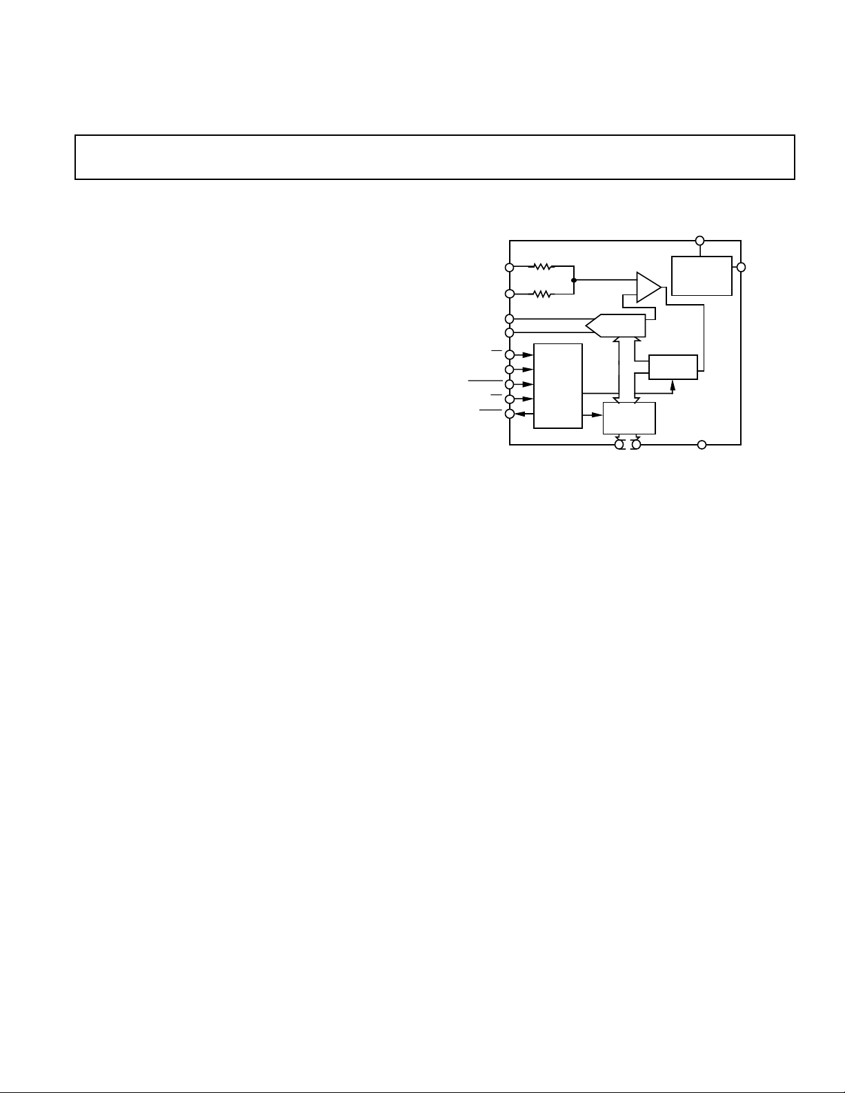
GENERAL DESCRIPTION
The AD7880 is a high speed, low power, 12-bit A/D converter
which operates from a single +5 V supply. It consists of a 3µs
track/hold amplifier, a 12 µs successive-approximation ADC,
versatile interface logic and a multiple-input-range circuit. The
part also includes a power save feature.
An internal resistor network allows the part to accept both unipolar and bipolar input signals while operating from a single
+5 V supply. Fast bus access times and standard control inputs
ensure easy interfacing to modern microprocessors and digital
signal processors.
The AD7880 features a total throughput time of 15 µs and can
convert full power signals up to 33 kHz with a sampling frequency of 66 kHz.
PRODUCT HIGHLIGHTS
1. Fast Conversion Time.
12 µs conversion time and 3 µs acquisition time allow for
large input signal bandwidth. This performance is ideally
suited for applications in areas such as telecommunications,
audio, sonar and radar signal processing.
2. Low Power Consumption.
2 mW power consumption in the power-down mode makes
the part ideally suited for portable, hand held, battery powered applications.
3. Multiple Input Ranges.
The part features three user-determined input ranges, 0 V to
+5 V, 0 V to 10 V and ± 5 V. These unipolar and bipolar
ranges are achieved with a 5 V only power supply.
In addition to the traditional dc accuracy specifications such as
linearity, full-scale and offset errors, the AD7880 is also fully
specified for dynamic performance parameters including harmonic distortion and signal-to-noise ratio.
The AD7880 is fabricated in Analog Devices’ Linear Compatible CMOS (LC
2
MOS) process, a mixed technology process
that combines precision bipolar circuits with low power CMOS
logic. The part is available in a 24-pin, 0.3 inch-wide, plastic or
hermetic dual-in-line package (DIP) as well as a small 24-lead
SOIC package.
REV. 0
Information furnished by Analog Devices is believed to be accurate and
reliable. However, no responsibility is assumed by Analog Devices for its
use, nor for any infringements of patents or other rights of third parties
which may result from its use. No license is granted by implication or
otherwise under any patent or patent rights of Analog Devices.
One Technology Way, P.O. Box 9106, Norwood, MA 02062-9106, U.S.A.
Tel: 617/329-4700 Fax: 617/326-8703
FUNCTIONAL BLOCK DIAGRAM
Page 2

AD7880–SPECIFICA TIONS
(VDD = +5 V 6 5%, V
unless otherwise noted. All Specifications T
= VDD, AGND = DGND = O V, f
REF
MIN
= 2.5 MHz, MODE = V
CLKIN
to T
unless otherwise noted.)
MAX
Parameter B Versions1C Versions1Units Test Conditions/Comments
DYNAMIC PERFORMANCE
2
Signal-to-Noise Ratio3 (SNR) 70 70 dB min Typically SNR Is 72 dB
Total Harmonic Distortion (THD) –80 –80 dB typ VIN = 1 kHz Sine Wave, f
VIN = 1 kHz Sine Wave, f
Peak Harmonic or Spurious Noise –80 –80 dB typ VIN = 1 kHz, f
SAMPLE
= 66 kHz
SAMPLE
SAMPLE
= 66 kHz
= 66 kHz
Intermodulation Distortion (IMD)
Second Order Terms –80 –80 dB typ fa = 0.983 kHz, fb = 1.05 kHz, f
Third Order Terms –80 –80 dB typ fa = 0.983 kHz, fb = 1.05 kHz, f
SAMPLE
SAMPLE
= 66 kHz
= 66 kHz
DC ACCURACY
Resolution 12 12 Bits All DC ACCURACY Specifications Apply for
the Three Analog Input Ranges
Integral Nonlinearity ± 1 ±1 LSB max
Differential Nonlinearity ± 1 ±1 LSB max Guaranteed Monotonic
Full-Scale Error ± 15 ± 5 LSB max
Bipolar Zero Error ±10 ±5 LSB max
Unipolar Offset Error ±5 ±5 LSB max
ANALOG INPUT
Input Voltage Ranges 0 to V
REF
0 to 2 V
±V
REF
Input Resistance 10 10 MΩ min 0 to V
5/12 5/12 kΩ min/max 8 kΩ typical: 0 to 2 V
5/12 5/12 kΩ min/max 8 kΩ typical: ± V
REF
0 to V
REF
0 to 2 V
±V
REF
Volts See Figure 5
Volts See Figure 6
REF
Volts See Figure 7
REF
Range
REF
Range
REF
Range
REFERENCE INPUT
V
(For Specified Performance) 5 5 V ±5%: Normally V
REF
I
REF
Nominal Reference Range 2.5/V
1.5 1.5 mA max
DD
2.5/V
DD
V min/max See Figure 3 for Degradation in Performance Down to 2.5 V
= VDD (See Reference Input Section)
REF
LOGIC INPUTS
CONVST, RD, CS, CLKIN
Input High Voltage, V
Input Low Voltage, V
Input Current, I
IN
Input Capacitance, C
INL
IN
INH
4
2.4 2.4 V min
0.8 0.8 V max
±10 ±10 µA max VIN = 0 V or V
10 10 pF max
DD
MODE INPUT
Input High Voltage, V
Input Low Voltage, V
Input Current, I
IN
Input Capacitance, C
INL
IN
INH
4
4 4 V min
1 1 V max
±125 ±125 µA max VIN = 0 V or V
10 10 pF max
DD
LOGIC OUTPUTS
DB11–DB0, BUSY
Output High Voltage, V
Output Low Voltage, V
OH
OL
4.0 4.0 V min I
0.4 0.4 V max I
SOURCE
= 1.6 mA
SINK
= 400 µA
DB11–DB0
Floating-State Leakage Current ±10 ±10 µA max
Floating-State Output Capacitance410 10 pF max
CONVERSION
Conversion Time 12 12 µs max f
CLKIN
= 2.5 MHz
Track/Hold Acquisition Time 3 3 µs max
POWER REQUIREMENTS
V
DD
I
DD
Normal Power Mode @ +25°C 7.5 7.5 mA max Typically 4 mA; MODE = V
T
to T
MIN
MAX
+5 +5 V nom ± 5% for Specified Performance
10 10 mA max Typically 5 mA; MODE = V
DD
DD
Power Save Mode @ +25°C 750 750 µA max Logic Inputs @ 0 V or VDD; MODE = 0 V
T
MIN
to T
MAX
1 1 mA max Logic Inputs @ 0 V or VDD; MODE = 0 V
Power Dissipation
Normal Power Mode @ +25°C 37.5 37.5 mW max VDD = 5 V: Typically 20 mW; MODE = V
T
MIN
to T
MAX
50 50 mW max VDD = 5 V: Typically 25 mW; MODE = V
Power Save Mode @ +25°C 3.75 3.75 mW max VDD = 5 V: Typically 2 mW; MODE = 0 V
T
to T
MIN
MAX
NOTES
1
Temperature ranges are as follows: B/C Versions, –40°C to +85°C.
2
VIN = 0 to V
3
SNR calculation includes distortion and noise components.
4
Sample tested @ +25°C to ensure compliance.
REF
5 5 mW max VDD = 5 V: Typically 2.5 mW; MODE = 0 V
Specifications subject to change without notice.
–2–
DD
DD
DD
REV. 0
Page 3
TIMING CHARACTERISTICS
1
(VDD = +5 V 6 5%, V
= VDD, AGND = DGND = 0 V)
REF
AD7880
Limit at +258C Limit at T
MIN
, T
MAX
Parameter (All Versions) (All Versions) Units Conditions/Comments
t
1
t
2
t
3
t
4
t
5
t
6
2
t
7
3
t
8
50 50 ns min CONVST Pulse Width
130 130 ns min CONVST to BUSY Falling Edge
0 0 ns min BUSY to CS Setup Time
0 0 ns min CS to RD Setup Time
0 0 ns min CS to RD Hold Time
60 75 ns min RD Pulse Width
57 70 ns max Data Access Time after RD
55 ns min Bus Relinquish Time after RD
50 50 ns max
NOTES
1
Timing specifications in bold print are 100% production tested. All other times are sample tested at +25°C to ensure compliance. All input signals are specified with
tr = tf = 5 ns (10% to 90% of 5 V) and timed from a voltage level of 1.6 V.
2
t7 is measured with the load circuit of Figure 2 and defined as the time required for an output to cross 0.8 V or 2.4 V.
3
t8 is derived from the measured time taken by the data outputs to change by 0.5 V when loaded with the circuit of Figure 2. The measured number is then extrapo-
lated back to remove the effects of charging the 50 pF capacitor. This means that the time, t8, quoted in the timing characteristics is the true bus relinquish time of
the part and as such is independent of external bus loading capacitances.
t
CONVST
BUSY
CS
RD
DB0 – DB11
1
TRACK/HOLD
GOES INTO HOLD
t
2
t
CONVERT
THREE-STATE
Figure 1. Timing Diagram
1.6mA
CS CONVST RD Function
1 1 X Not Selected
t
3
1 j 1 Start Conversion g
0 1 0 Enable ADC Data
0 1 1 Data Bus Three Stated
t
t
4
5
t
6
ABSOLUTE MAXIMUM RATINGS*
VDD to AGND . . . . . . . . . . . . . . . . . . . . . . . . . –0.3 V to +7 V
t
t
8
7
DATA
VALID
V
to DGND . . . . . . . . . . . . . . . . . . . . . . . . . –0.3 V to +7 V
DD
AGND to DGND . . . . . . . . . . . . . . . . . –0.3 V to V
V
, V
INA
V
INA
V
INA
V
REF
to AGND (Figure 5) . . . . . . –0.3 V to VDD + 0.3 V
INB
to AGND (Figure 6) . . . . . . . . . –0.6 V to 2 VDD + 0.6 V
to AGND (Figure 7) . . . . . –VDD – 0.3 V to V
to AGND . . . . . . . . . . . . . . . . . . . . . . . . . . 0.3 V to V
Digital Inputs to DGND . . . . . . . . . . . –0.3 V to VDD + 0.3 V
Digital Outputs to DGND . . . . . . . . . . –0.3 V to V
Table I. Truth Table
+ 0.3 V
DD
+ 0.3 V
DD
+ 0.3 V
DD
DD
Operating Temperature Range
TO OUTPUT
PIN
50pF
200µA
2.1V+
Figure 2. Load Circuit for Access and Relinquish Time
Industrial (B, C Versions) . . . . . . . . . . . . . –40°C to +85°C
Storage Temperature Range . . . . . . . . . . . –65°C to +150°C
Lead Temperature (Soldering, 10 secs) . . . . . . . . . . . . +300°C
Power Dissipation (Any Package) to +75°C . . . . . . . . 450 mW
Derates above +75°C by . . . . . . . . . . . . . . . . . . . . . 10 mW/°C
*Stresses above those listed under “Absolute Maximum Ratings” may cause
permanent damage to the device. This is a stress rating only and functional
operation of the device at these or any other conditions above those listed in the
operational sections of this specification is not implied. Exposure to absolute
maximum rating conditions for extended periods may affect device reliability.
CAUTION
ESD (electrostatic discharge) sensitive device. Electrostatic charges as high as 4000 V readily
accumulate on the human body and test equipment and can discharge without detection.
Although the AD7880 features proprietary ESD protection circuitry, permanent damage may
occur on devices subjected to high energy electrostatic discharges. Therefore, proper ESD
precautions are recommended to avoid performance degradation or loss of functionality.
REV. 0
–3–
WARNING!
ESD SENSITIVE DEVICE
Page 4
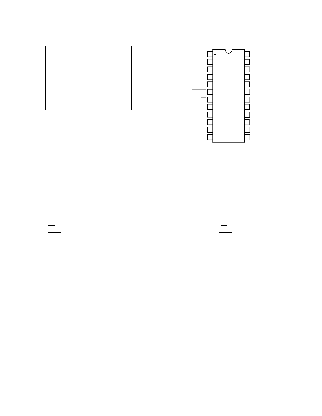
AD7880
TOP VIEW
(Not to Scale)
1
2
3
4
5
6
7
8
9
10
11
12
13
14
24
23
22
21
20
19
18
17
16
15
AD7880
AGND
CLKIN
DGND
DB0
DB1 DB2
DB3
DB4
DB5
DB6
V
DD
DB8
V
INA
V
INB
DB7
DB9
DB10
DB11
MODE
CS
CONVST
RD
BUSY
V
REF
ORDERING GUIDE
PIN CONFIGURATION
Bipolar
Full-Scale Zero
Temperature Error Error Package
Model Range (LSBs) (LSBs) Option*
AD7880BN –40°C to +85°C ±15 ±10 N-24
AD7880BQ –40°C to +85°C ±15 ±10 Q-24
AD7880CN –40°C to +85°C ±5 ±5 N-24
AD7880CQ –40°C to +85°C ±5 ±5 Q-24
AD7880BR –40°C to +85 °C ±15 ±10 R-24
AD7880CR –40°C to +85°C ±5 ±5 R-24
*N = Plastic DIP; Q = Cerdip; R = SOIC (Small Outline Integrated Circuit).
PIN FUNCTION DESCRIPTION
Pin Pin
No. Mnemonic Function
1V
2V
INA
INB
Analog Input.
Analog Input.
3 AGND Analog Ground.
4V
5
6
7
8
REF
CS Chip Select. Active Low Logic input. The device is selected when this input is active.
CONVST Convert Start. A low to high transition on this input puts the track/hold into hold mode and starts con-
RD Read. Active Low Logic Input. This input is used in conjunction with CS low to enable data outputs.
BUSY Active Low Logic Output. This status line indicates converter status. BUSY is low during conversion.
Voltage Reference Input. This is normally tied to VDD.
version. This input is asynchronous to the CLKIN and is independent of
CS and RD.
9 CLKIN Clock Input. TTL-compatible logic input. Used as the clock source for the A/D converter. The mark/
space ratio of the clock can vary from 40/60 to 60/40.
10 DGND Digital Ground.
11 . . . 22 DB0–DB11 Three-State Data Outputs. These become active when
CS and RD are brought low.
23 MODE MODE Input. This input is used to put the device into the power save mode (MODE = 0 V). During
24 V
DD
normal operation, the MODE input will be a logic high (MODE = V
Power Supply. This is nominally +5 V.
DD
).
–4–
REV. 0
Page 5
AD7880
+
–
R
R
SAMPLING
COMPARATOR
V
INA
V
INB
V
REF
AGND
12-BIT DAC
0 TO V
REF
V
REF
= 0 TO 2V
REF
V
IN
CIRCUIT INFORMATION
The AD7880 is a +5 V single supply 12-bit A/D converter. The
part requires no external components apart from a 2.5 MHz external clock and power supply decoupling capacitors. It contains
a 12-bit successive approximation ADC based on a fast-settling
voltage-output DAC, a high speed comparator and SAR, as well
as the necessary control logic. The charge balancing comparator
used in the AD7880 provides the user with an inherent trackand-hold function. The ADC is specified to work with sampling
rates up to 66 kHz.
CONVERTER DETAILS
The AD7880 conversion cycle is initiated on the rising edge of
the CONVST pulse, as shown in the timing diagram of Figure
1. The rising edge of the
CONVST pulse places the track/hold
amplifier into “HOLD” mode. The conversion cycle then takes
between 26 and 28 clock periods. The maximum specified conversion time is 12 µs. This corresponds to a conversion cycle
time of 28 clock periods with a CLKIN frequency of 2.5 MHz
and also includes internal propagation delays. During conversion the
BUSY output will remain low, and the output databus
drivers will be three-stated. When a conversion is completed,
the
BUSY output will go to a high level, and the result of the
conversion can be read by bringing
CS and RD low.
The track/hold amplifier acquires a 12-bit input signal in 3µs.
The overall throughput time for the AD7880 is equal to the
conversion time plus the track/hold acquisition time. For a
2.5 MHz input clock the throughput time is 15 µs.
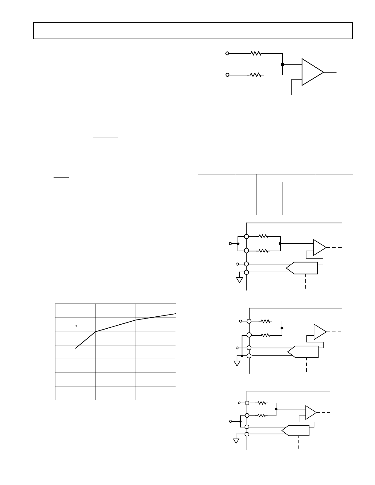
REFERENCE INPUT
For specified performance, it is recommended that the reference
input be tied to V
. The part, however, will operate with a ref-
DD
erence down to 2.5 V though with reduced performance specifications. Figure 3 shows a graph of signal-to-noise ratio (SNR)
versus V
V
REF
.
REF
must not be allowed to go above VDD by more than
100 mV.
74
F = 51.2kHz
S
72
F = 2.525kHz
IN
T = 25 C
A
70
V
INA
+
R
V
INB
R
–
V
DAC
Figure 4. AD7880 Input Circuit
The AD7880 accommodates three separate input ranges, 0 to
V
, 0 to 2 V
REF
REF
and ±V
. The input configurations corre-
REF
sponding to these ranges are shown in Figures 5, 6 and 7.
With V
= VDD and using a nominal VDD of +5 V, the input
REF
ranges are 0 V to 5 V, 0 V to 10 V and +5 V, as shown in
Table II.
Table II. Analog Input Ranges
Analog Input
Range V
0 V to +5 V V
0 V to +10 V V
±5 V V
= 0 TO V
V
IN
REF
V
REF
Figure 5. 0 to V
Input Connections
V
REF
DD
DD
DD
INA
V
IN
V
IN
V
IN
R
V
INA
R
V
INB
V
REF
AGND
Unipolar Input Configuration
REF
V
INB
V
IN
AGND Figure 6
V
REF
0 TO V
12-BIT DAC
Connection
Diagram
Figure 5
Figure 7
SAMPLING
COMPARATOR
REF
+
–
68
– dBs
66
SNR
64
62
60
2345
Figure 3. SNR vs. V
ANALOG INPUT
The AD7880 has two analog input pins, V
4 shows the input circuitry to the ADC sampling comparator.
The on-board attenuator network, made up of equal resistors,
allows for various input ranges.
REV. 0
V
REF
– Volts
REF
INA
and V
INB
. Figure
–5–
Figure 6. 0 to 2 V
±
= V
V
REF
IN
V
REF
Figure 7.±V
V
INA
V
INB
V
REF
AGND
REF
Unipolar Input Configuration
REF
0 TO V
REF
12-BIT DAC
SAMPLING
COMPARATOR
+
–
R
R
Bipolar Input Configuration
Page 6

AD7880
2.5
2.0
1.5
1.0
0.5
0.0
0.5
1.5 2.5 3.5
CLOCK FREQUENCY – MHz
NORMALIZED LINEARITY ERROR
The AD7880 has two unipolar input ranges, 0V to 5 V and 0 V
to 10 V. Figure 5 shows the analog input for the 0V to 5 V
range. The designed code transitions occur midway between
successive integer LSB values (i.e., 1/2 LSB, 3/2 LSBs,
5/2 LSBs . . . FS –3/2 LSBs). The output code is straight binary
with 1 LSB = FS/4096 = 5 V/4096 = 1.22 mV. The same applies
for the 0 V to 10 V range, as shown in Figure 6, except that the
LSB size is bigger. In this case 1 LSB = FS/4096 = 10 V/4096 =
2.44 mV. The ideal input/output transfer characteristic for both
these unipolar ranges is shown in Figure 8.
OUTPUT
CODE
111...111
111...110
111...101
111...100
000...011
000...010
000...001
000...000
1LSB
0V
V INPUT VOLTAGE
IN
1LSB =
FS
4096
+
FS – 1LSB
Figure 8. AD7880 Unipolar Transfer Characteristic
Figure 7 shows the AD7880’s ± 5 V bipolar analog input configuration. Once again the designed code transitions occur midway between successive integer LSB values. The output code is
straight binary with 1 LSB = FS/4096 = 10 V/4096 = 2.44mV.
The ideal bipolar input/output transfer characteristic is shown in
Figure 9.
OUTPUT
CODE
111...111
111...110
100...101
100...000
011...111
011...110
000...001
000...000
–
FS
2
–
1LSB
1LSB+
0V
V INPUT VOLTAGE
IN
FS = 10V
1LSB =
+
4096
FS
2
1LSB–
FS
CLOCK INPUT
The AD7880 is specified to operate with a 2.5MHz clock connected to the CLKIN input pin. This pin may be driven directly
by CMOS or TTL buffers. The mark/space ratio on the clock
can vary from 40/60 to 60/40. As the clock frequency is slowed
down, it can result in slightly degraded accuracy performance.
This is due to leakage effects on the hold capacitor in the internal track-and-hold amplifier. Figure 10 is a typical plot of accuracy versus clock frequency for the ADC.
Figure 10. Normalized Linearity Error vs. Clock Frequency
TRACK/HOLD AMPLIFIER
The charge balanced comparator used in the AD7880 for the
A/D conversion provides the user with an inherent track/hold
function. The track/hold amplifier acquires an input signal to
12-bit accuracy in less than 3 µs. The overall throughput time is
equal to the conversion time plus the track/hold amplifier acquisition time. For a 2.5 MHz input clock, the throughput time is
15 µs.
The operation of the track/hold amplifier is essentially transparent to the user. The track/hold amplifier goes from its tracking
mode to its hold mode at the start of conversion, i.e., on the rising edge of
CONVST as shown in Figure 1.
OFFSET AND FULL-SCALE ADJUSTMENT
In most Digital Signal Processing (DSP) applications, offset and
full-scale errors have little or no effect on system performance.
Offset error can always be eliminated in the analog domain by
ac coupling. Full-scale error effect is linear and does not cause
problems as long as the input signal is within the full dynamic
range of the ADC. Some applications will require that the input
signal range match the maximum possible dynamic range of the
ADC. In such applications, offset and full-scale error will have
to be adjusted to zero.
The following sections describe suggested offset and full-scale
adjustment techniques which rely on adjusting the inherent offset of the op amp driving the input to the ADC as well as tweaking an additional external potentiometer as shown in Figure 11.
Figure 9. AD7880 Bipolar Transfer Characteristic
–6–
REV. 0
Page 7

AD7880
R1
10 kΩ
V
1
R2
500 Ω
R3
10 kΩ
*ADDITIONAL PINS OMITTED FOR CLARITY
+
–
10 kΩ
R5
10 kΩ
V
R4
INA
AD7880*
AGND
Figure 11. Offset and Full-Scale Adjust Circuit
Unipolar Adjustments
In the case of the 0 V to 5 V unipolar input configuration, unipolar
offset error must be adjusted before full-scale error. Adjustment is
achieved by trimming the offset of the op amp driving the analog input of the AD7880. This is done by applying an input
voltage of 0.61 mV (1/2 LSB) to V
in Figure 11 and adjusting
1
the op amp offset voltage until the ADC output code flickers
between 0000 0000 0000 and 0000 0000 0001. For full-scale
adjustment, an input voltage of 4.9982 V (FS–3/2 LSBs) is
applied to V
and R2 is adjusted until the output code flickers
1
between 1111 1111 1110 and 1111 1111 1111.
The same procedure is required for the 0 V to 10 V input con-
figuration of Figure 6. An input voltage of 1.22 mV (1/2 LSB) is
applied to V
in Figure 11 and the op amp’s offset voltage is
1
adjusted until the ADC output code flickers between 0000 0000
0000 and 0000 0000 0001. For full-scale adjustment, an input
voltage of 9.9963 V (FS–3/2 LSBs) is applied to V
and R2 is
1
adjusted until the output code flickers between 1111 1111 1110
and 1111 1111 1111.
Bipolar Adjustments
Bipolar zero and full-scale errors for the bipolar input configuration of Figure 7 are adjusted in a similar fashion to the unipolar
case. Again, bipolar zero error must be adjusted before full-scale
error. Bipolar zero error adjustment is achieved by trimming the
offset of the op amp driving the analog input of the AD7880
while the input voltage is 1/2 LSB below ground. This is done
by applying an input voltage of –1.22 mV (1/2 LSB) to V
in
1
Figure 11 and adjusting the op amp offset voltage until the
ADC output code flickers between 0111 1111 1111 and 1000
0000 0000. For full-scale adjustment, an input voltage of
4.9982 V (FS/2–3/2 LSBs) is applied to V
and R2 is adjusted
1
until the output code flickers between 1111 1111 1110 and
1111 1111 1111.
DYNAMIC SPECIFICATIONS
The AD7880 is specified and tested for dynamic performance
specifications as well as traditional dc specifications such as
integral and differential nonlinearity. The ac specifications are
required for signal processing applications such as speech recognition, spectrum analysis and high speed modems. These applications require information on the ADC’s effect on the spectral
content of the input signal. Hence, the parameters for which the
AD7880 is specified include SNR, harmonic distortion, intermodulation distortion and peak harmonics. These terms are discussed in more detail in the following sections.
Signal-to-Noise Ratio (SNR)
SNR is the measured signal-to-noise ratio at the output of the
ADC. The signal is the rms magnitude of the fundamental.
Noise is the rms sum of all the nonfundamental signals up to
half the sampling frequency (FS/2) excluding dc. SNR is dependent upon the number of quantization levels used in the digitization process; the more levels, the smaller the quantization
noise. The theoretical signal to noise ratio for a sine wave input
is given by:
SNR = (6.02 N + 1.76) dB (1)
where N is the number of bits.
Thus for an ideal 12-bit converter, SNR = 74 dB.
The output spectrum from the ADC is evaluated by applying a
sine wave signal of very low distortion to the V
input which is
IN
sampled at a 66 kHz sampling rate. A Fast Fourier Transform
(FFT) plot is generated from which the SNR data can be obtained. Figure 12 shows a typical 2048 point FFT plot of the
AD7880 with an input signal of 2.5 kHz and a sampling frequency of 61 kHz. The SNR obtained from this graph is 73dB.
It should be noted that the harmonics are taken into account
when calculating the SNR.
Figure 12. FFT Plot
Effective Number of Bits
The formula given in Equation 1 relates the SNR to the number
of bits. Rewriting the formula, as in Equation 2, it is possible to
get a measure of performance expressed in effective number of
bits (N).
SNR −1. 76
N =
6.02
(2)
The effective number of bits for a device can be calculated
directly from its measured SNR.
Figure 13 shows a plot of effective number of bits versus input
frequency for an AD7880 with a sampling frequency of 61 kHz.
The effective number of bits typically remains better than 11.5
for frequencies up to 12 kHz.
REV. 0
–7–
Page 8

AD7880
12
11.5
11
10.5
EFFECTIVE NUMBER OF BITS
10
INPUT FREQUENCY – kHz
SAMPLE FREQUENCY = 61kHz
T = 25 C
A
15 30.5
Figure 13. Effective Number of Bits vs. Frequency
Total Harmonic Distortion (THD)
THD is the ratio of the rms sum of harmonics to the rms value
of the fundamental. For the AD7880, THD is defined as:
2
2
2
2
+V
+V
V
2
THD = 20log
3
where V
V
is the rms amplitude of the fundamental and V2, V3,
1
, V5 and V6 are the rms amplitudes of the second through the
4
+V
4
V
1
2
+V
5
6
(3)
sixth harmonic. The THD is also derived from the FFT plot of
the ADC output spectrum.
Intermodulation Distortion
With inputs consisting of sine waves at two frequencies, fa and
fb, any active device with nonlinearities will create distortion
products at sum and difference frequencies of mfa ± nfb where
m, n = 0, 1, 2, 3, etc. Intermodulation terms are those for which
neither m nor n are equal to zero. For example, the second order terms include (fa + fb) and (fa – fb), while the third order
terms include (2fa + fb), (2fa – fb), (fa + 2fb) and (fa – 2fb).
Using the CCIF standard where two input frequencies near the
top end of the input bandwidth are used, the second and third
order terms are of different significance. The second order terms
are usually distanced in frequency from the original sine waves,
while the third order terms are usually at a frequency close to
the input frequencies. As a result, the second and third order
terms are specified separately. The calculation of the intermodulation distortion is as per the THD specification where it is
the ratio of the rms sum of the individual distortion products to
the rms amplitude of the fundamental expressed in dBs. In this
case, the input consists of two, equal amplitude, low distortion,
sine waves. Figure 14 shows a typical IMD plot for the
AD7880.
Figure 14. IMD Plot
Peak Harmonic or Spurious Noise
Peak harmonic or spurious noise is defined as the ratio of the
rms value of the next largest component in the ADC output
spectrum (up to FS/2 and excluding dc) to the rms value of the
fundamental. Normally, the value of this specification will be
determined by the largest harmonic in the spectrum, but for
parts where the harmonics are buried in the noise floor the peak
will be a noise peak.
–8–
REV. 0
Page 9

AD7880
MICROPROCESSOR INTERFACING
The AD7880 high speed bus timing allows direct interfacing to
real time digital signal processors, DSPs, as well as modern high
speed, 16-bit microprocessors. Suitable microprocessor interfaces are shown in Figures 15 through 20.
AD7880–ADSP-2100 Interface
Figure 15 shows an interface between the AD7880 and the
ADSP-2100. Conversion is initiated using a timer to drive the
CONVST input asynchronously to the microprocessor. This allows very accurate control of the sampling instant. When conversion is complete, the AD7880
inverter on this
BUSY output drives the IRQ line low thus pro-
BUSY line goes high. An
viding an interrupt to the ADSP-2100 when conversion is completed. The conversion result is then read from the AD7880 into
the ADSP-2100 with the following instruction:
MR0 = DM(ADC)
where MR0 is the ADSP-2100 MR0 Register and
where ADC is the AD7880 address.
DMA13
DMA0
DMS
ADSP-2100
(ADSP-2101/
ADSP-2102)
DMRD (RD)
IRQn
DMD15
DMD0
ADDRESS BUS
ADDR
DECODE
EN
DATA BUS
* ADDITIONAL PINS OMITTED FOR CLARITY
CS
RD
BUSY
DB11
DB0
TIMER
CONVST
AD7880*
Figure 15. AD7880–ADSP-2100 (ADSP-2101/ADSP-2102)
Interface
AD7880-ADSP-2101/ADSP-2102 Interface
The interface outlined in Figure 15 also forms the basis for an
interface between the AD7880 and the ADSP-2101/ADSP-2102.
The READ line of the ADSP-2101/ADSP-2102 is labeled
In this interface, the
RD pulse width of the processor can be
RD.
programmed using the Data Memory Wait State Control Register. The instruction used to read a conversion result is as outlined for the ADSP-2100.
AD7880-TMS32010 Interface
An interface between the AD7880 and the TMS32010 is shown
in Figure 16. Once again the conversion is initiated using an external timer and the TMS32010 is interrupted when conversion
is completed. The following instruction is used to read the conversion result from the AD7880:
IN D,ADC
where D is Data Memory Address and
where ADC is the AD7880 address.
TIMER
PA2
ADDRESS BUS
PA0
TMS32010
ADDR
DECODE
MEN
DEN
INT
D15
D0
EN
DATA BUS
*ADDITIONAL PINS OMITTED FOR CLARITY
CONVST
CS
AD7880*
RD
BUSY
DB11
DB0
Figure 16. AD7880–TMS32010 Interface
AD7880–TMS320C25 Interface
Figure 17 shows an interface between the AD7880 and the
TMS320C25. As with the two previous interfaces, conversion is
initiated with a timer, and the processor is interrupted when the
conversion sequence is completed. The TMS320C25 does not
have a separate
rectly. This has to be generated from the processor
R/
W outputs with the addition of some logic gates. The RD sig-
nal is OR-gated with the
RD output to drive the AD7880 RD input di-
STRB and
MSC signal to provide the one WAIT
state required in the read cycle for correct interface timing.
Conversion results are read from the AD7880 using the following instruction:
IN D,ADC
where D is Data Memory Address and
where ADC is the AD7880 address.
TIMER
A15
TMS320C25
INTn
STRB
R/W
READY
MSC
D15
ADDRESS BUS
A0
ADDR
DECODE
IS
D0
EN
DATA BUS
*ADDITIONAL PINS OMITTED FOR CLARITY
CONVST
CS
BUSY
RD
DB11
DB0
AD7880*
Figure 17. AD7880–TMS320C25 Interface
Some applications may require that the conversion be initiated
by the microprocessor rather than an external timer. One option
is to decode the AD7880
CONVST from the address bus so that
REV. 0
–9–
Page 10

AD7880
a write operation starts a conversion. Data is read at the end of
the conversion sequence as before. Figure 19 shows an example
of initiating conversion using this method. A similar implementation can be used for DSPs. Note that for all interfaces, a read
operation should not be attempted during conversion.
AD7880–MC68000 Interface
An interface between the AD7880 and the MC68000 is shown
in Figure 18. As before, conversion is initiated using an external
timer. The AD7880
processor or, alternatively, software delays can ensure that conversion has been completed before a read to the AD7880 is attempted. Because of the nature of its interrupts, the 68000
requires additional logic (not shown in Figure 18) to allow it to
be interrupted correctly. For further information on 68000 interrupts, consult the 68000 users manual.
The MC68000
separate
the 68000
RD input signal for the AD7880. CS is used to drive
DTACK input to allow the processor to execute a
normal read operation to the AD7880. The conversion results
are read using the following 68000 instruction:
MOVE.W ADC, D0
where D0 is the 68000 D0 register
where ADC is the AD7880 address
MC68000
BUSY line can be used to interrupt the
AS and R/W outputs are used to generate a
A15
A0
AS EN
ADDRESS BUS
ADDR
DECODE
TIMER
CONVST
CS
ADDRESS BUS
8086
LATCHALE
WR
RD
AD15
AD0
*ADDITIONAL PINS OMITTED FOR CLARITY
ADDR
DECODE
ADDRESS/DATA BUS
CS
AD7880*
CONVST
RD
DB11
DB0
Figure 19. AD7880–8086 Interface
AD7880–6809 Interface
The AD7880 can also interface quite easily with 8-bit microprocessors. The 12-bit parallel data output from the AD7880
can be read into the microprocessor as an 8+4 byte structure.
Figure 20 shows an interface to the MC6809 8-bit microprocessor. As in previous cases, conversion is initiated using an external timer. At the end of conversion,
which drives the
IRQ interrupt input of the microprocessor. A
BUSY triggers a one-shot
double read is then performed to two unique addresses. The
first read fetches the lower 8 bits (DB0–DB7) and loads the
74HC374 latch with the upper 4 bits (DB8–DB11). The second read fetches these upper 4 bits.
DTACK
R/W
D15
D0
DATA BUS
*ADDITIONAL PINS OMITTED FOR CLARITY
AD7880*
RD
DB11
DB0
Figure 18. AD7880–MC68000 Interface
AD7880–8086 Interface
Figure 19 shows an interface between the AD7880 and the
8086 microprocessor. Unlike the previous interface examples,
the microprocessor initiates conversion. This is achieved by gating the 8086
ent to the AD7880
WR signal with a decoded address output (differ-
CS address). Conversion is initiated and the
result is read from the AD7880 using the following instruction:
MOV AX, ADC
where AX is the 8086 accumulator and
where ADC is the AD7880 address
A15
A0
MC6809
R/W
IRQ
D7
D0
ADDRESS BUS
ADDR
DECODE
E
OE
Q0
DATA BUS
*ADDITIONAL PINS OMITTED FOR CLARITY
CLK
D3
Q3
D0
74HC374
ONE
SHOT
Figure 20. AD7880–6809 Interface
CS
AD7880*
RD
BUSY
DB11
DB8
DB7
DB0
TIMER
CONVST
–10–
REV. 0
Page 11

V+
+
–
C1
10µF
C2
0.1µF
IC1
ANALOG
INPUT
V+
V–
AB
V–
AB
LK2
LK3
TO ADC
LK1
SKT1
A
C3
10µF
C4
0.1µF
A
V+
V
DD
01
2
TIME – secs
POWER
CONSUMPTION – mW
20
2
CONVERTING
POWER-DOWN
CONVERTING
POWER-DOWN
A
A
A
A
1.65 x 10
4–
APPLICATION HINTS
Good printed circuit board (PCB) layout is as important as the
circuit design itself in achieving high speed A/D performance.
The AD7880’s comparator is required to make bit decisions on
an LSB size of 1.22 mV. To achieve this, the designer must be
conscious of noise both in the ADC itself and in the preceding
analog circuitry. Switching mode power supplies are not recommended, as the switching spikes will feed through to the comparator causing noisy code transitions. Other causes of concern
are ground loops and digital feedthrough from microprocessors.
These are factors which influence any ADC, and a proper PCB
layout which minimizes these effects is essential for best
performance.
LAYOUT HINTS
Ensure that the layout for the printed circuit board has the digital and analog signal lines separated as much as possible. Take
care not to run digital tracks alongside analog signal tracks.
Guard (screen) the analog input with AGND.
Establish a single point analog ground (star ground) separate
from the logic system ground at the AD7880 AGND pin or as
close as possible to the AD7880. Connect all other grounds and
the AD7880 DGND to this single analog ground point. Do not
connect any other digital grounds to this analog ground point.
Low impedance analog and digital power supply common returns are essential to low noise operation of the ADC, so make
the foil width for these tracks as wide as possible. The use of
ground planes minimizes impedance paths and also guards the
analog circuitry from digital noise. The circuit layout of Figures 26 and 27 have both analog and digital ground planes
which are kept separated and only joined together at the
AD7880 AGND pin.
NOISE
Keep the input signal leads to VIN and signal return leads from
AGND as short as possible to minimize input noise coupling. In
applications where this is not possible, use a shielded cable between the source and the ADC. Reduce the ground circuit impedance as much as possible since any potential difference in
grounds between the signal source and the ADC appears as an
error voltage in series with the input signal.
ANALOG INPUT BUFFERING
To achieve specified performance, it is recommended that the
analog input (V
INA
, V
) be driven from a low impedance
INB
source. This necessitates the use of an input buffer amplifier.
The choice of op amp will be a function of the particular application and the desired analog input range. The data acquisition
circuit, described in this data sheet allows for various op amp
configurations. Figure 21 shows the analog input buffer circuit.
The options available to drive the supply of the op amp are:
Single +5 V (derived from PCB 5 V supply)
Dual Supply (externally supplied to V+ and V–)
±5 V, ±12 V or ±15 V
The simplest configuration is the 0 V to 5 V range of Figure 5.
A single supply 5 V op amp is recommended for such an implementation. This will allow for operation of the AD7880 in the 0
V to 5 V unipolar range without supplying an external supply to
V+ and V–. The 5 V supply is derived from the systems
+5 V V
REV. 0
supply.
DD
AD7880
Figure 21. Analog Input Buffering
When it is required to drive the AD7880 with the 0 V to 10 V
input range, an external supply must be connected to V+ (see
Figure 21).
In bipolar operation, positive and negative supplies must be
connected to V+ and V–.
The AD711 is a general purpose op amp which could be used
to drive the analog input of the AD7880.
POWER-DOWN CONTROL (MODE INPUT)
The AD7880 is designed for systems which need to have minimum power consumption. This includes such applications as
hand held, portable battery powered systems and remote monitoring systems. As well as consuming minimum power under
normal operating conditions, typically 20 mW, the AD7880
can be put into a power-down or sleep mode when not required
to convert signals. When in this power-down mode, the
AD7880 consumes approximately 2 mW of power.
The AD7880 is powered down by bringing the MODE input
pin to a Logic Low in conjunction with keeping the
control High. The AD7880 will remain in the power-down
mode until MODE is brought to a Logic High again. The
MODE input should be driven with CD4000 or HCMOS logic
levels.
It is recommended that one “dummy” conversion be implemented before reading conversion data from the AD7880 after
it has been in the power-down mode. This is required to reset
all internal logic and control circuitry. In a remote monitoring
system where, say, 10 conversions are required to be taken with
a sampling interval of 1 second, an additional 11th conversion
must be carried out. Figure 22 gives a plot of power consumption
A
A
A
A
Figure 22. Power Consumption for Normal Operation
and Power-Down Operation vs. Time
–11–
RD input
Page 12

AD7880
as a function of time for such operation. The total conversion
time for each cycle is 11 × 15 µs (where 15 µs is the time taken
for a single conversion) corresponding to 1.65 × 10
–4
secs.
Hence:
Average Power = Power
CONVERTING
+ Power
POWER-DOWN
= {20 mW × (1.65 × 10–4)/(10)}
+ {2 mW × (9.9998)/(10)}
= 2.029 mW
AD7880 DATA ACQUISITION LAYOUT
Figure 24 shows the AD7880 in a data acquisition circuit. The
corresponding printed circuit board (PCB) layout and
silkscreen are shown in Figures 25 to 27.
The only additional component required for a full data acquisition system is an antialiasing filter. There is a component grid
provided near the analog input on the PCB which may be used
for such a filter or any other input conditioning circuitry. To facilitate this option there is a shorting link (labeled LK1 on the
PCB) on the analog input track. With LK1 in place, the analog
input connects to the buffer amplifier driving the AD7880.
With LK1 removed, a wire link is needed to connect the analog
input to the PCB component grid.
INTERFACE CONNECTIONS
The data acquisition board contains a parallel connection port
labeled SKT4. This is a 26-contact IDC Connector and provides for direct microprocessor connection to the board. This
connector, the pinout of which is shown in Figure 23, contains
all data, control and status signals of the AD7880 (with the exception of the
CONVST and the CLKIN inputs both of which
are provided via SKT2 and SKT3 respectively). It also contains
decoded R/
W and STRB inputs which are necessary for interfacing to many microprocessors including the TMS320C25 and
the Motorola 68000 series. Link LK7 selects
ternatively, the decoded version. Note that the AD7880
RD directly or al-
CS in-
put must be decoded prior to the AD7880 evaluation board.
SKT1, SKT2 and SKT3 are three sub-miniature connectors
(SMC) which provide input connections for the analog input,
the
CONVST input and the CLKIN input. Three different input ranges can be accepted by the AD7880 each of which is
configured by selecting shorting plug options A, B or C of LK4.
Position A corresponds to the 0 V to 5 V unipolar configuration
of Figure 5, position B corresponds to the bipolar ± 5 V configuration of Figure 7 and position C allows for a 0 V to +10 V unipolar range as shown in Figure 6.
POWER SUPPLY CONNECTIONS
The PCB requires a single +5 V power supply (labeled VDD).
Good decoupling allows this supply to drive the AD7880 V
which also drives the V
input as well as the op amp power
REF
DD
supply. In circumstances where bipolar ± 5 V or a unipolar 0 V
to 10 V input ranges are required, provision has been allowed
for the connection of separate op amp power supplies (± 15 V,
±12 V, ±5 V, etc.) to V+ and V–. LK2 and LK3 shorting links
allow for the selection of user defined op amp power supplies or
the on-board single +5 V supply.
LINK OPTIONS
There are seven link options which must be set before using the
board. These are outlined below:
–12–
LK1 Connects the analog input to a buffer amplifier. The
analog input may also be connected to a component
grid for signal conditioning.
LK2, LK3 Allows for various op amp power supplies to be
used to drive the input buffer of the AD7880. External supplies may be connected to V+ and V–.
Alternatively, the AD7880’s +5 V system supply
and AGND can be selected to drive a single supply
op amp.
LK4 Configures the various analog input ranges, 0 V to
5 V, 0 V to 10 V or ±5 V.
LK5 Selects reference input to V
mally connected to V
DD
of AD7880. Nor-
REF
. An external reference
could also be wired in.
LK6 Selects power-down or sleep mode. The shorting
plug is connected to V
LK7 Connects the AD7880
input of SKT4 or to a decoded
for normal operation.
DD
RD input directly to the RD
STRB and R/W
input. This shorting plug setting depends on the
microprocessor, e.g., the TMS320C25 requires a
decoded
RD signal.
1
R/W
3
RD
5
CS
BUSY
7
9
N/C
DB10
11
13
DB8
15
DB6
DB4
17
DB2
19
DB0
21
+
23
5V
GND
25
2
STRB
N/C
4
6
N/C
8
BUSY
N/C
10
12 DB11
14
DB9
16
DB7
DB5
18
DB3
20
DB1
22
+
24
5V
26
GND
Figure 23. SKT4, IDC Connector Pinout
COMPONENT LIST
IC1 Op Amp*
IC2 AD7880 Analog-to-Digital Converter
IC3 74HC00 Quad NAND Gate
C1, C3, C5 10 µF Capacitors
C2, C4, C6, C7 0.1 µF Capacitors
R1, R2 10 kΩ Pull-up Resistors
LK1, LK2, LK3 Shorting Links
LK4, LK5, LK6
LK7
SKT1, SKT2, SKT3 Sub-Miniature Connectors
Vendor No: Sealectro 50-051-0000 (Socket)
Vendor No: Sealectro 50-007-0000 (Plug)
SKT4 26-Contact (2 Row) IDC Connector
NOTE
*See ANALOG INPUT BUFFERING section.
.
REV. 0
Page 13

AD7880
Figure 24. Data Acquisition Circuit Using the AD7880
REV. 0
Figure 25. PCB Silkscreen for Figure 24
–13–
Page 14

AD7880
Figure 26. PCB Component Side Layout for Figure 24
Figure 27. PCB Solder Side Layout for Figure 24
–14–
REV. 0
Page 15

OUTLINE DIMENSIONS
24
1
12
13
0.295
(7.493)
MAX
SEATING
PLANE
0.021 (0.533)
0.015 (0.381)
TYP
0.225
(5.715)
MAX
1.290 (32.77) MAX
0.125
(3.175)
MIN
0.110 (2.794)
0.009 (2.286)
TYP
0.070 (1.778)
0.020 (0.508)
0.065 (1.651)
0.055 (1.397)
15°
0°
0.320 (8.128)
0.291 (7.4)
0.012 (0.305)
0.008 (0.203)
0.180
(4.572)
MAX
1. LEAD NO. 1 IDENTIFIED BY DOT OR NOTCH.
2. CERDIP LEADS WILL BE EITHER TIN PLATED OR SOLDER DIPPED
IN ACCORDANCE WITH MIL-M-38510 REQUIREMENTS.
Dimensions shown in inches and (mm).
24-Lead Plastic DIP (N-24)
1.228 (31.19)
1.226 (31.14)
24
112
0.130 (3.30)
0.128 (3.25)
SEATING
PLANE
PIN 1
0.02 (0.5)
0.016 (0.41)
NOTES:
1. LEAD NO. 1 IDENTIFIED BY DOT OR NOTCH.
2. PLASTIC LEADS WILL BE EITHER SOLDER DIPPED OR TIN LEAD PLATED
IN ACCORDANCE WITH MIL-M-38510 REQUIREMENTS.
0.11 (2.79)
0.09 (2.28)
0.07 (1.78)
0.05 (1.27)
13
0.260 ± 0.001
(6.61 ± 0.03)
24-Lead Cerdip (Q-24)
0.32 (8.128)
0.30 (7.62)
15°
0
AD7880
0.011 (0.28)
0.009 (0.23)
REV. 0
0.419 (10.65)
0.394 (10.00)
0.614 (15.6)
0.598 (15.2)
24 13
PIN 1
0.012 (0.3)
0.004 (0.1)
0.05
(1.27)
BSC
24-Lead SOIC (R-24)
0.299 (7.6)
0.291 (7.4)
121
0.104 (2.65)
0.093 (2.35)
0.019 (0.49)
0.014 (0.35)
0.013 (0.32)
0.009 (0.23)
–15–
0.03 (0.75)
0.01 (0.25)
8°
0°
0.05 (1.27)
0.016 (0.40)
Page 16

C1414–10–6/90
–16–
PRINTED IN U.S.A.
 Loading...