

Page 1
Low Voltage Controller for Touch Screens
AD7879W
Rev. 0
Trademarks and registered trademarks are the property of their respective owners.
Fax: 781.461.3113 ©2011 Analog Devices, Inc. All rights reserved.
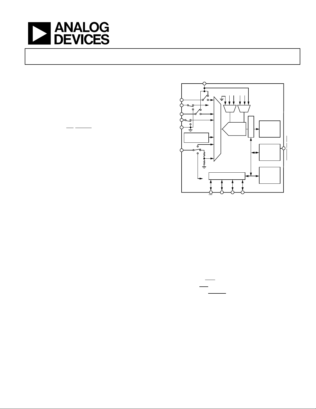
REF+
X– Y– X+ Y+
FIL
TERING
RESULT
REGISTERS
CONTROL
REGISTERS
SEQUENCER
AND TIMER
REF–
TEMPERATURE
SENSOR
TO
RESULT
REGISTERS
6-TO-1 MUX
AD7879W/
AD7879-1W
VCC/REF
X+
X–
Y+
Y–
GND
AUX/VBAT/GPIO
PENIRQ/INT/DAV
SERIAL PORT
DIN/
ADD1
DOUT/
SDA
SCL
CS/
ADD0
12-BIT
SAR ADC
REF–
10408-001
Data Sheet
FEATURES
4-wire touch screen interface
Qualified for automotive applications
1.6 V to 3.6 V operation
Median and averaging filter to reduce noise
Automatic conversion sequencer and timer
User-programmable conversion parameters
Auxiliary analog input/battery monitor (0.5 V to 5 V)
1 optional GPIO
Interrupt outputs (
INT, PENIRQ
Touch-pressure measurement
Wake-up on touch function
Shutdown mode: 6 µA maximum
16-lead, 4.4 mm × 5 mm TSSOP
16-lead, 4 mm × 4 mm LFCSP
APPLICATIONS
Automotive applications
Personal digital assistants
Smart handheld devices
Touch screen monitors
Point-of-sale terminals
Medical devices
Cell phones
)
FUNCTIONAL BLOCK DIAGRAM
Figure 1.
GENERAL DESCRIPTION
The AD7879W is a 12-bit successive approximation analog-todigital converters (SAR ADCs) with a synchronous serial
interface and low on-resistance switches for driving 4-wire
resistive touch screens. The AD7879W works with a very low
power supply—a single 1.6 V to 3.6 V supply—and feature
throughput rates of 105 kSPS. The devices include a shutdown
mode that reduces current consumption to less than 6 µA.
To reduce the effects of noise from LCDs and other sources, the
AD7879W contains a preprocessing block. The preprocessing
function consists of a median filter and an averaging filter. The
combination of these two filters provides a more robust solution,
discarding the spurious noise in the signal and keeping only the
data of interest. The size of both filters is programmable. Other
user-programmable conversion controls include variable
acquisition time and first conversion delay; up to 16 averages
can be taken per conversion. The AD7879W can run in slave
Information furnishe d by Analog Devices is believed to be accurate and reliable. However, no
responsibility is assumed by Analog Devices for its use, nor for any infringements of patents or other
rights of third parties that may result from its use. Specifications subject to change without notice. No
license is granted by implication or otherwise under any patent or patent rights of Analog Devices.
mode or standalone (master) mode, using an automatic
conversion sequencer and timer.
The AD7879W has a programmable pin that can operate as an
auxiliary input to the ADC, as a battery monitor, or as a GPIO.
In addition, a programmable interrupt output can operate in
three modes: as a general-purpose interrupt to signal when new
data is available (
are exceeded (
screen is touched (
DAV
), as an interrupt to indicate when limits
INT
), or as a pen-down interrupt when the
PENIRQ
). The AD7879W offers temperature
measurement and touch-pressure measurement.
The AD7879W is available in a 16-lead, 4.4 mm × 5.0 mm
TSSOP and 16-lead 4 mm × 4 mm LFCSP. Both packages
support an SPI interface (AD7879W) or an I
2
C® interface
(AD7879-1W).
One Technology Way, P.O. Box 9106, Norwood, MA 02062-9106, U.S.A.
Tel: 781.329.4700
www.analog.com
Page 2

AD7879W Data Sheet
TABLE OF CONTENTS
Features .............................................................................................. 1
Applications ....................................................................................... 1
Functional Block Diagram .............................................................. 1
General Description ......................................................................... 1
Revision History ............................................................................... 2
Specifications ..................................................................................... 3
SPI Timing Specifications (AD7879W) .................................... 4
I2C Timing Specifications (AD7879-1W) .................................. 5
Absolute Maximum Ratings ............................................................ 6
Thermal Resistance ...................................................................... 6
ESD Caution .................................................................................. 6
Pin Configurations and Function Descriptions ........................... 7
Typical Performance Characteristics ............................................. 9
Terminology .................................................................................... 12
Theory of Operation ...................................................................... 13
Touch Screen Principles ............................................................ 13
Measuring Touch Screen Inputs ............................................... 14
Touch -Pressure Measurement .................................................. 15
Temperature Measurement ....................................................... 15
Median and Averaging Filters ....................................................... 17
AUX/VBAT/GPIO Pin ................................................................... 18
Auxiliary Input ............................................................................ 18
Battery Input ............................................................................... 18
Limit Comparison ...................................................................... 18
GPIO ............................................................................................ 18
Conversion Timing ........................................................................ 20
Register Map ................................................................................... 21
Detailed Register Descriptions ..................................................... 22
Control Registers ............................................................................ 26
Control Register 1 ...................................................................... 26
Control Register 2 ...................................................................... 28
Control Register 3 ...................................................................... 29
Interrupts ..................................................................................... 30
Synchronizing the AD7879W to the Host CPU .................... 31
Serial Interface ................................................................................ 32
SPI Interface ................................................................................ 32
I2C-Compatible Interface .......................................................... 34
Grounding and Layout .................................................................. 37
Lead Frame Chip Scale Packages ............................................. 37
Outline Dimensions ....................................................................... 38
Ordering Guide .......................................................................... 39
Automotive Products ................................................................. 39
REVISION HISTORY
12/11—Revision 0: Initial Version
Rev. 0 | Page 2 of 40
Page 3

Data Sheet AD7879W
Internal Clock Accuracy
1.8 2.2
MHz
SPECIFICATIONS
VCC = 1.6 V to 3.6 V, TA = −40°C to +85°C, unless otherwise noted.
Table 1.
Parameter Min Typ Max Unit Test Conditions/Comments
DC ACCURACY
Resolution 12 Bits
No Missing Codes 11 12 Bits
Integral Nonlinearity (INL)1 ±3 LSB LSB size = 390 µV.
Differential Nonlinearity (DNL)1 LSB size = 390 µV.
Negative DNL −0.99 LSB
Positive DNL 2 LSB
Offset Error
Gain Error
Noise3 70 µV rms
Power Supply Rejection3 60 dB
Internal Clock Frequency 2 MHz
SWITCH DRIVERS
On Resistance1
Y+, X+ 6 Ω
Y−, X− 5 Ω
ANALOG INPUTS
Input Voltage Range 0 VCC V
DC Leakage Current ±0.1 µA
Input Capacitance 30 pF
Accuracy 0.3 %
TEMPERATURE MEASUREMENT
Temperature Range −40 +85 °C
Resolution 0.3 °C
Accuracy2 ±2 °C Calibrated at 25°C.
BATTERY MONITOR
Input Voltage Range 0.5 5 V
Input Impedance3 16 kΩ
Accuracy 2 5 % Uncalibrated accuracy.
LOGIC INPUTS (DIN, SCL, CS, SDA, GPIO)
Input High Voltage, V
Input Low Voltage, V
Input Current, IIN 0.01 µA VIN = 0 V or VCC.
Input Capacitance, C
LOGIC OUTPUTS (DOUT, GPIO, SCL, SDA,
Output High Voltage, VOH VCC − 0.2 V
Output Low Voltage, VOL 0.4 V
Floating-State Leakage Current ±0.1 µA
Floating-State Output Capacitance2 5 pF
CONVERSION RATE3
Conversion Time 9.5 µs Including 2 µs of acquisition time, MAV
Throughput Rate 105 kSPS
1, 2
±2 ±6 LSB
1, 2
±4 LSB
0.7 × VCC V
INH
0.3 × VCC V
INL
3
10 pF
IN
)
INT
filter off. 2 µs of additional time is required
if MAV filter is on.
Rev. 0 | Page 3 of 40
Page 4
AD7879W Data Sheet
Static
406 µA
ADC and temperature sensor are off; the
t6
20
ns max
DOUT access time after SCL falling edge
CS
SCL
DIN
DOUT
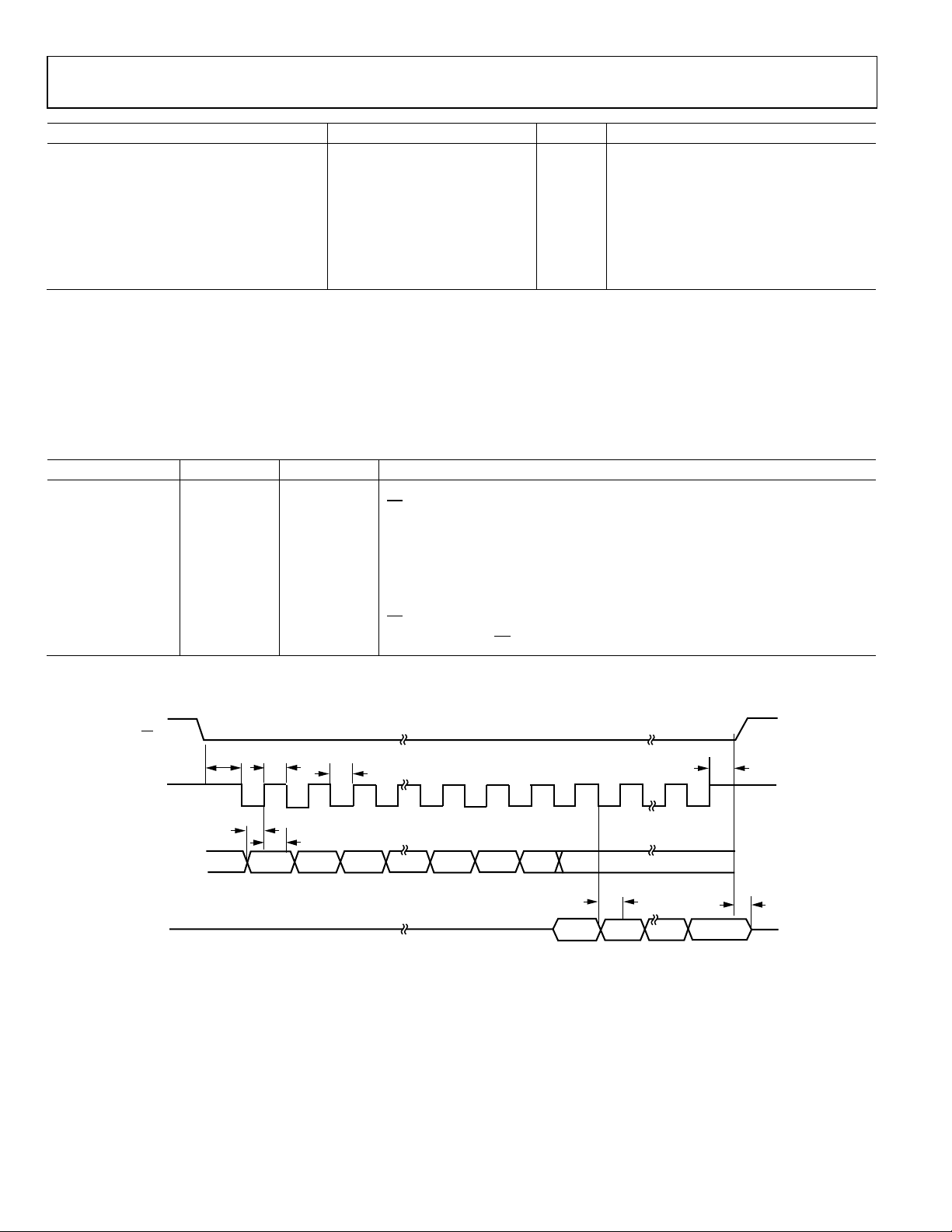
t
1
1
16
15
MSB
LSB
2 3
MSB
LSB
1 2
15
16
t
2
t
4
t
5
t
3
t
6
t
7
t
8
10408-002
Parameter Min Typ Max Unit Test Conditions/Comments
POWER REQUIREMENTS
VCC 1.6 2.6 3.6 V Specified performance.
ICC Digital inputs = 0 V or VCC.
Converting Mode 480 650 µA ADC on, PM = 10.
reference and oscillator are on; PM = 01
or 11.
Shutdown Mode 0.5 6 µA PM = 00.
1
See the Terminology section.
2
Guaranteed by characterization; not production tested.
3
Sample tested at 25°C to ensure compliance.
SPI TIMING SPECIFICATIONS (AD7879W)
VCC = 1.6 V to 3.6 V, TA = −40°C to +85°C, unless otherwise noted. Sample tested at 25°C to ensure compliance. All input signals are
specified with t
Table 2.
Parameter1 Limit Unit Description
f
5 MHz max
SCL
t1 5 ns min
t2 20 ns min SCL high pulse width
t3 20 ns min SCL low pulse width
t4 15 ns min DIN setup time
t5 15 ns min DIN hold time
= tF = 5 ns (10% to 90% of VCC) and timed from a voltage level of 1.4 V.
R
falling edge to first SCL falling edge
CS
t7 16 ns max
t8 15 ns min SCL rising edge to CS high
1
Guaranteed by design; not production tested.
rising edge to DOUT high impedance
CS
Figure 2. Detailed SPI Timing Diagram
Rev. 0 | Page 4 of 40
Page 5
Data Sheet AD7879W
S
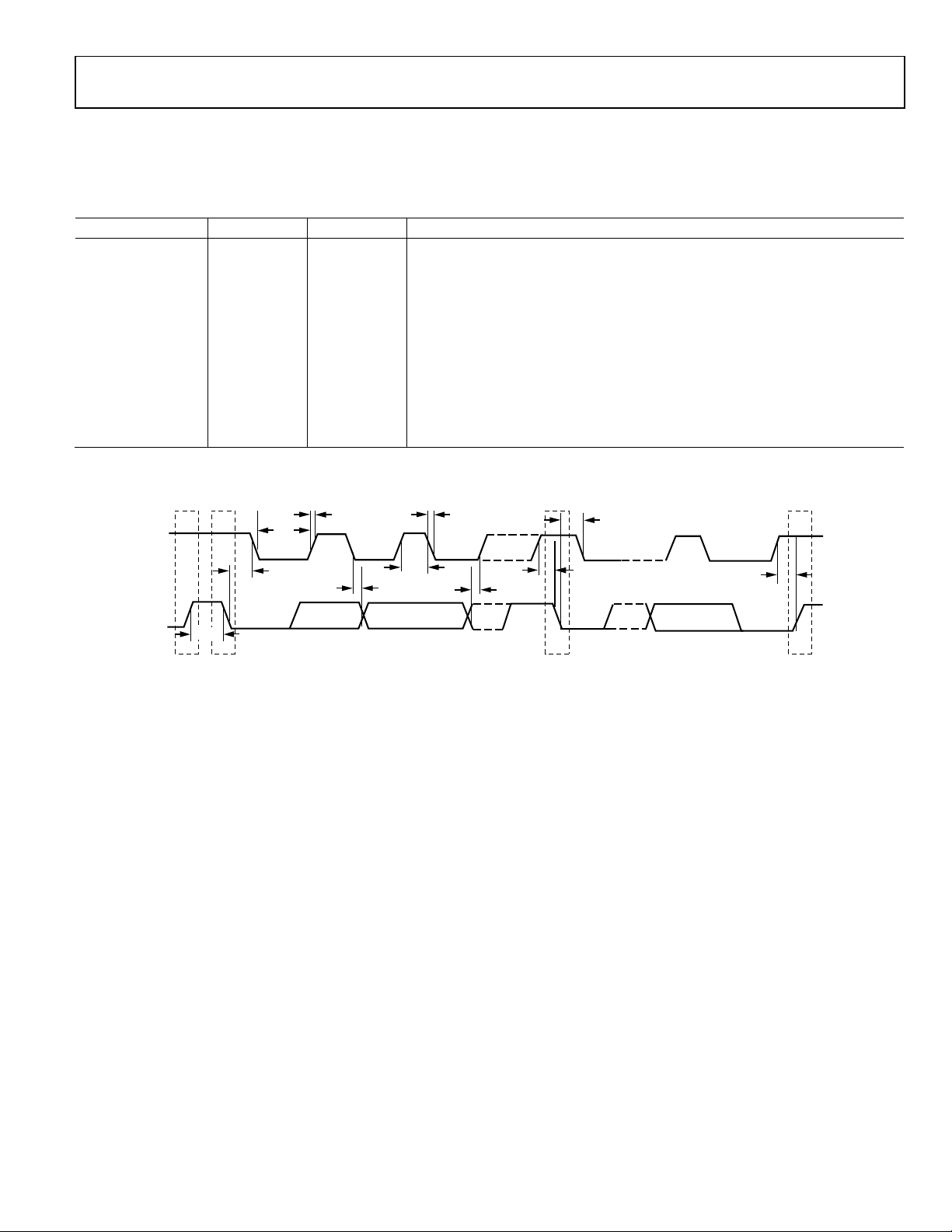
I2C TIMING SPECIFICATIONS (AD7879-1W)
VCC = 1.6 V to 3.6 V, TA = −40°C to +85°C, unless otherwise noted. Sample tested at 25°C to ensure compliance. All input signals are
timed from a voltage level of 1.4 V.
Table 3.
Parameter1 Limit Unit Description
f
400 kHz max
SCL
t1 0.6 μs min Start condition hold time, t
t2 1.3 μs min Clock low period, t
t3 0.6 μs min Clock high period, t
t4 100 ns min Data setup time, t
t5 300 ns min Data hold time, t
LOW
SU; DAT
HD; DAT
HIGH
t6 0.6 μs min Stop condition setup time, t
t7 0.6 μs min Start condition setup time, t
t8 1.3 μs min Bus-free time between stop and start conditions, t
tR 300 ns max Clock/data rise time
tF 300 ns max Clock/data fall time
1
Guaranteed by design; not production tested.
SCL
DA
t
t
2
t
1
t
8
R
t
5
t
F
t
3
t
4
HD; STA
SU; STO
SU; STA
t
7
BUF
t
1
t
6
STOP START STOPSTART
Figure 3. Detailed I
2
C Timing Diagram
10408-003
Rev. 0 | Page 5 of 40
Page 6
AD7879W Data Sheet
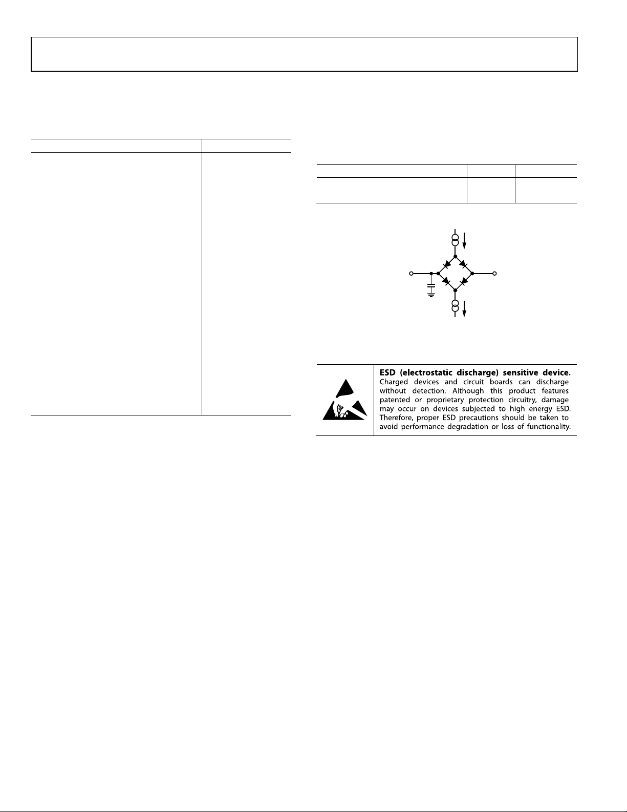
ESD Rating (X+, Y+, X−, Y−)
16-Lead LFCSP
30.4
°C/W
200µA I
OL
200µA I
OH
1.4V
TO OUTPUT
PIN
C
L
50pF
10408-004
ABSOLUTE MAXIMUM RATINGS
TA = 25°C, unless otherwise noted.
Table 4.
Parameter Rating
VCC to GND −0.3 V to +3.6 V
Analog Input Voltage to GND −0.3 V to VCC + 0.3 V
AUX/VBAT to GND −0.3 V to +5 V
Digital Input Voltage to GND −0.3 V to VCC + 0.3 V
Digital Output Voltage to GND −0.3 V to VCC + 0.3 V
Input Current to Any Pin Except Supplies1 10 mA
Air Discharge Human Body Model 15 kV
Contact Human Body Model 10 kV
ESD Rating (All Other Pins)
Human Body Discharge 4 kV
Field-Induced Charged Device Model 1 kV
Machine Model 0.2 kV
Operating Temperature Range −40°C to +85°C
Storage Temperature Range −65°C to +150°C
Junction Temperature 150°C
Power Dissipation
TSSOP (4-Layer Board) 577.2 mW
LFCSP (4-Layer Board) 2.138 W
IR Reflow Peak Temperature 260°C (±0.5°C)
Lead Temperature (Soldering 10 sec) 300°C
1
Transient currents of up to 100 mA do not cause SCR latch-up.
THERMAL RESISTANCE
θJA is specified for the worst-case conditions, that is, a device
soldered in a circuit board for surface-mount packages.
Table 5. Thermal Resistance
Package Type1 θJA Unit
16-Lead TSSOP 112.6 °C/W
1
4-layer board.
Figure 4. Circuit Used for Digital Timing
ESD CAUTION
Stresses above those listed under Absolute Maximum Ratings
may cause permanent damage to the device. This is a stress
rating only; functional operation of the device at these or any
other conditions above those indicated in the operational
section of this specification is not implied. Exposure to absolute
maximum rating conditions for extended periods may affect
device reliability.
Rev. 0 | Page 6 of 40
Page 7
Data Sheet AD7879W
5 5 X−
Touch Screen Input Channel.
NC = NO CONNECT
1
2
3
4
5
6
7
8
NC
X+
Y+
NC
Y–
X–
V
CC
/REF
DIN
16
15
14
13
12
11
10
9
NC
AUX/VBAT/GPIO
PENIRQ/INT/DAV
NC
GND
SCL
DOUT
CS
AD7879W
TOP VIEW
(Not to S cale)
10408-005
NC = NO CONNECT
1
2
3
4
5
6
7
8
NC
X+
Y+
NC
Y–
X–
V
CC
/REF
ADD1
16
15
14
13
12
11
10
9
NC
AUX/VBAT/GPIO
PENIRQ/INT/DAV
NC
GND
SCL
SDA
ADD0
AD7879W
TOP VIEW
(Not to S cale)
10408-006
PIN CONFIGURATIONS AND FUNCTION DESCRIPTIONS
Figure 5. AD7879W TSSOP Pin Configuration
Figure 6. AD7879-1W TSSOP Pin Configuration
Table 6. Pin Function Descriptions, TSSOP
Pin No.
AD7879W AD7879-1W
Mnemonic Description
1 1 VCC/REF Power Supply Input and ADC Reference.
2, 7, 10, 15 2, 7, 10, 15 NC No Connect.
3 3 X+ Touch Screen Input Channel.
4 4 Y+ Touch Screen Input Channel.
6 6 Y− Touch Screen Input Channel.
8 N/A DIN SPI Serial Data Input to the AD7879W.
N/A 8 ADD1 I2C Address Bit 1 for the AD7879-1W. This pin can be tied high or low to determine an
address for the AD7879-1W (see Table 25).
9 9 GND Ground. Ground reference point for all circuitry on the AD7879W. All analog input signals
and any external reference signal should be referred to this voltage.
11 11 SCL Serial Interface Clock Input.
12 N/A DOUT SPI Serial Data Output for the AD7879W.
N/A 12 SDA I2C Serial Data Input and Output for the AD7879-1W.
13 13
PENIRQ/INT
DAV
/
Interrupt Output. This pin is asserted when the screen is touched (
ment exceeds the preprogrammed limits (
(
). Active low, internal 50 kΩ pull-up resistor.
DAV
), or when new data is available in the registers
INT
), when a measure-
PENIRQ
14 14 AUX/VBAT/GPIO This pin can be programmed as an auxiliary input to the ADC (AUX), as a battery measure-
ment input to the ADC (VBAT), or as a general-purpose digital input/output (GPIO).
16 N/A
Chip Select for the SPI Serial Interface on the AD7879W. Active low.
CS
N/A 16 ADD0 I2C Address Bit 0 for the AD7879-1W. This pin can be tied high or low to determine an
address for the AD7879-1W (see Table 25).
Rev. 0 | Page 7 of 40
Page 8
AD7879W Data Sheet
16
16
X+
Touch Screen Input Channel.
PIN 1
INDICATOR
1Y+
2NC
3NC
4X–
11 NC
12
10 NC
9 DOUT
5
Y–
6
DIN
7
GND
8
SCL
15
V
CC
/REF
16
X+
14
13
AUX/VBAT/GPIO
AD7879W
TOP VIEW
(Not to S cale)
PENIRQ/INT/DAV
CS
NOTES
1. NC = NO CONNECT
2. THE EXPOSED PAD IS NOT CONNECTED INTERNALLY.
FOR INCREAS E D RE LIABILI TY OF THE SOLDER JOINTS
AND MAXIMUM T HE RM AL CAPABILITY, IT IS RECOMMENDED
THAT THE PAD BE SOLDERED TO T HE GROUND PLANE.
10408-007
PIN 1
INDICATOR
1Y+
2NC
3NC
4X–
11 NC
12
10 NC
9 SDA
5
Y–
6
ADD1
7
GND
8
SCL
15
V
CC
/REF
16
X+
14
13
AUX/VBAT/GPIO
AD7879-1W
TOP VIEW
(Not to S cale)
PENIRQ/INT/DAV
ADD0
NOTES
1. NC = NO CONNECT
2. THE EXPOSED PAD IS NOT CONNECTED INTERNALLY.
FOR INCREAS E D RE LIABILI TY OF THE SOLDER JOINTS
AND MAXIMUM T HE RM AL CAPABILITY, IT IS RECOMMENDED
THAT THE PAD BE SOLDERED TO T HE GROUND PLANE.
10408-008
Figure 7. AD7879W LFCSP Pin Configuration
Figure 8. AD7879-1W LFCSP Pin Configuration
Table 7. Pin Function Descriptions, LFCSP
Pin No.
AD7879W AD7879-1W
Mnemonic Description
1 1 Y+ Touch Screen Input Channel.
2, 3, 10, 11 2, 3, 10, 11 NC No Connect.
4 4 X− Touch Screen Input Channel.
5 5 Y− Touch Screen Input Channel.
6 N/A DIN SPI Serial Data Input to the AD7879W.
N/A 6 ADD1 I2C Address Bit 1 for the AD7879-1W. This pin can be tied high or low to determine an
address for the AD7879-1W (see Table 25).
7 7 GND Ground. Ground reference point for all circuitry on the AD7879W. All analog input signals
and any external reference signal should be referred to this voltage.
8 8 SCL Serial Interface Clock Input.
9 N/A DOUT SPI Serial Data Output for the AD7879W.
N/A 9 SDA I2C Serial Data Input and Output for the AD7879-1W.
12 12
PENIRQ/INT/DAV
Interrupt Output. This pin is asserted when the screen is touched (
ment exceeds the preprogrammed limits (
(
). Active low, internal 50 kΩ pull-up resistor.
DAV
), or when new data is available in the registers
INT
), when a measure-
PENIRQ
13 13 AUX/VBAT/GPIO This pin can be programmed as an auxiliary input to the ADC (AUX), as a battery measure-
ment input to the ADC (VBAT), or as a general-purpose digital input/output (GPIO).
14 N/A
Chip Select for the SPI Serial Interface on the AD7879W. Active low.
CS
N/A 14 ADD0 I2C Address Bit 0 for the AD7879-1W. This pin can be tied high or low to determine an
address for the AD7879-1W (see Table 25).
15 15 VCC/REF Power Supply Input and ADC Reference.
EP Exposed Pad. The exposed pad is not connected internally. For increased reliability of the
solder joints and maximum thermal capability, it is recommended that the pad be
soldered to the ground plane.
Rev. 0 | Page 8 of 40
Page 9
Data Sheet AD7879W
475
470
465
460
455
450
445
440
435
430
425
–40 –25 –10 10 25 40 55 70 85
TEMPERATURE (°C)
CURRENT (µA)
10408-009
700
600
500
400
300
200
100
0
1.6 1.8 2.0 2.2 2.4 2.6 2.8 3.0 3.2 3.4 3.6
V
CC
(V)
CURRENT (µA)
10408-010
4.0
3.5
3.0
2.5
2.0
1.5
1.0
0.5
0
–40 –25 –10 10 25 50 75 100
TEMPERATURE (°C)
CURRENT (µA)
10408-011
1.0
–1.0
–0.8
–0.6
–0.4
–0.2
0
0.2
0.4
0.6
0.8
TEMPERATURE (°C)
GAIN ERROR V ARIATION (LSB)
2.6V
3.6V
1.6V
85–40 –25 –10 10 25 40 55 70
10408-012
1.0
–1.0
–0.8
–0.6
–0.4
–0.2
0
0.2
0.4
0.6
0.8
TEMPERATURE (°C)
OFFSET VARIATION (LSB)
2.6V
3.6V
1.6V
85
–40 –25 –10 10
25 40 55 70
10408-013
2.0
–2.0
–1.5
–1.0
–0.5
0
0.5
1.0
1.5
0 4096358430722560204815361024512
CODE
INL (LSB)
10408-014
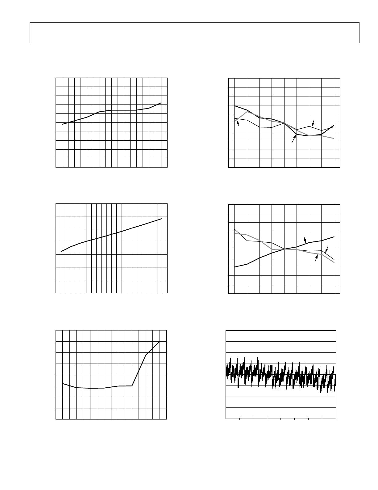
TYPICAL PERFORMANCE CHARACTERISTICS
TA = 25°C, VCC = 2.6 V, f
= 2 MHz, unless otherwise noted.
SCL
Figure 9. Supply Current vs. Temperature
Figure 10. Supply Current vs. VCC
Figure 12. Change in ADC Gain vs. Temperature
Figure 13. Change in ADC Offset vs. Temperature
Figure 11. Full Power-Down IDD vs. Temperature
Figure 14. ADC INL
Rev. 0 | Page 9 of 40
Page 10
AD7879W Data Sheet
1.0
0.8
0.6
0.4
0.2
0
–0.2
–0.4
–0.6
–0.8
–1.0
1 501 1001 1501 2001 2501 3001 3501 4001
CODE
DNL (LSB)
10408-015
7
6
5
4
3
2
1
0
1.6 1.8 2.0 2.2 2.4 2.6 2.8 3.0 3.2 3.4 3.6
V
CC
(V)
R
ON
(Ω)
X+ TO V
CC
Y+ TO V
CC
X– TO GND
Y– TO GND
10408-016
6.0
5.5
5.0
4.5
4.0
3.5
3.0
–40 –25 –10 10 25 40 55 70 85
TEMPERATURE (°C)
R
ON
(Ω)
X+ TO V
CC
Y+ TO V
CC
X– TO GND
Y– TO GND
10408-017
2370
2369
2368
2367
2366
2365
2364
2363
2362
2361
2360
–40 –25 –15 –5 5 15 25 35 45 55 65
TEMPERATURE (°C)
ADC CODE (Decimal )
75 85
10408-018
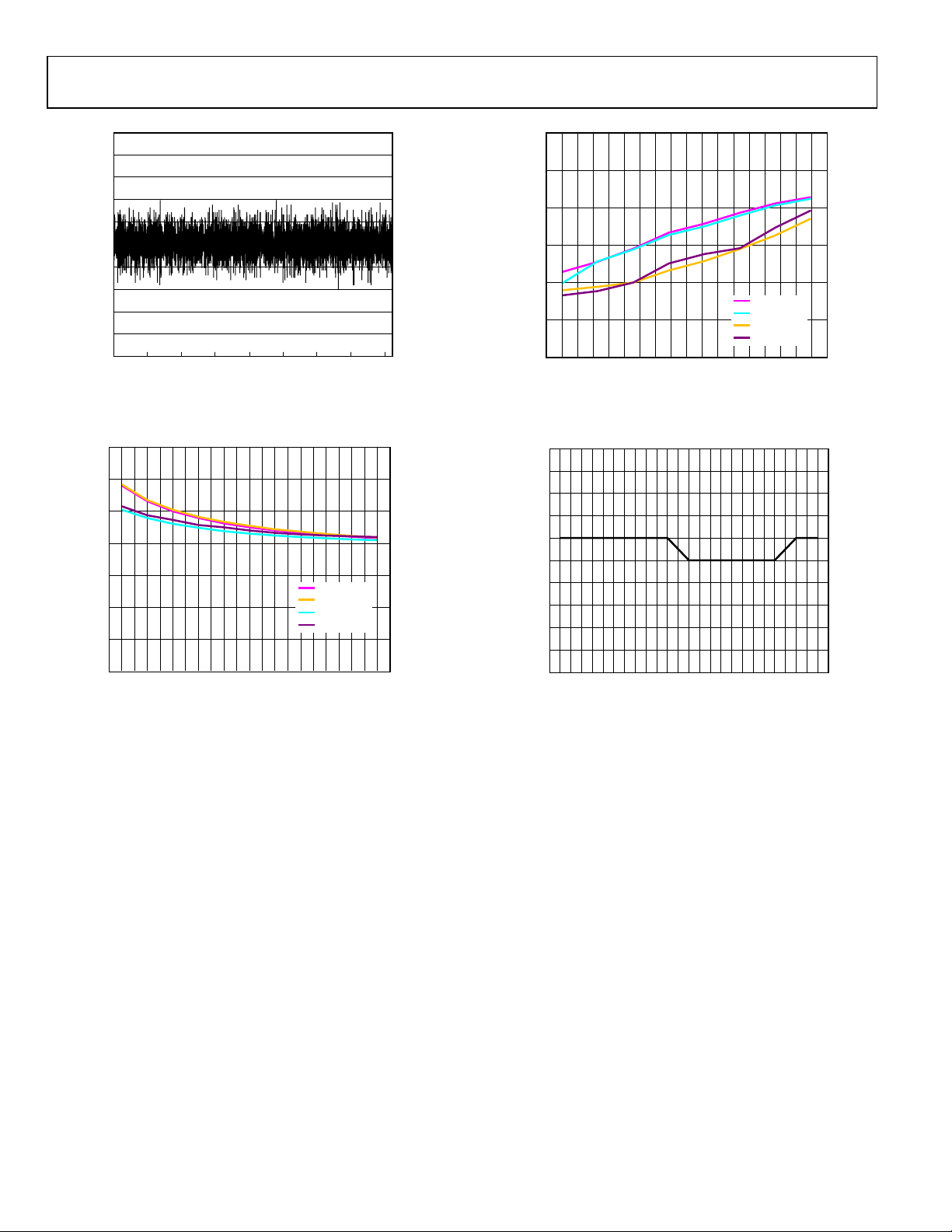
Figure 15. ADC DNL
Figure 16. Switch On Resistance vs. VCC
(X+, Y+: Pin to V
; X−, Y−: Pin to GND)
CC
Figure 17. Switch On Resistance vs. Temperature
(X+, Y+: Pin to V
; X−, Y−: Pin to GND)
CC
Figure 18. ADC Code vs. Temperature (Fixed Analog Input)
Rev. 0 | Page 10 of 40
Page 11
Data Sheet AD7879W
1400
1200
1000
800
600
400
200
0
2.2 2.3 2.4 2.5 2.6 2.7 2.8 2.9 3.0 3.1 3.2 3.3 3.4 3.5 3.6
V
CC
(V)
TEMPERAT URE ( Code)
10408-019
0
–20
–40
–60
–80
–100
–120
–140
–160
0
1603
3206
4809
6412
8015
9618
11221
12824
14427
16030
17633
19236
20839
22442
24045
25648
27251
28854
30457
32060
33663
35266
36869
FREQUENCY ( Hz )
INPUT TONE AMPLITUDE (dB)
SNR = 61.58dB
THD = 72.34dB
10408-020
250
200
150
100
50
0
NUMBER OF UNI TS
–4 –3 –2 –1 0
ERROR (%)
MEAN: –1.98893
SD: 0.475534
10408-021
Figure 19. Temperature Code vs. VCC for 25°C
Figure 21. Typical Uncalibrated Accuracy for the Battery Channel (25°C)
Figure 20. Typical FFT Plot for the Auxiliary Channels at 25 kHz Sampling
Rate and 1 kHz Input Frequency
Rev. 0 | Page 11 of 40
Page 12

AD7879W Data Sheet
TERMINOLOGY
Differential Nonlinearity (DNL)
DNL is the difference between the measured and the ideal
1 LSB change between any two adjacent codes in the ADC.
Integral Nonlinearity (INL)
INL is the maximum deviation from a straight line passing
through the endpoints of the ADC transfer function. The
endpoints of the transfer function are zero scale at 1 LSB below
the first code transition and full scale at 1 LSB above the last
code transition.
Gain Error
Gain error is the deviation of the last code transition
(111 … 110 to 111 … 111) from the ideal (V
after the offset error has been calibrated out.
Offset Error
Offset error is the deviation of the first code transition
(00 … 000 to 00 … 001) from the ideal (AGND + 1 LSB).
On Resistance
On resistance is a measure of the ohmic resistance between the
drain and the source of the switch drivers.
− 1 LSB)
REF
Rev. 0 | Page 12 of 40
Page 13

Data Sheet AD7879W
X+
X–
Y–
Y+
CONDUCTIVE E LECTRODE
ON BOTTOM SIDE
PLASTIC FILM WITH
TRANSPARENT, RESISTIVE
COATING ON BOTTOM SIDE
PLASTIC FILM WITH
TRANSPARENT, RESISTIVE
COATING ONTOP SIDE
LCD SCREEN
CONDUCTIVE E LECTRODE
ON TOP SIDE
10408-022
THEORY OF OPERATION
The AD7879W is a complete 12-bit data acquisition system for
digitizing positional inputs from a 4-wire resistive touch screen.
To support this function, data acquisition on the AD7879W is
highly programmable to ensure accurate and noise-free results
from the touch screen.
The core of the AD7879W is a high speed, low power, 12-bit
analog-to-digital converter (ADC) with an input multiplexer,
on-chip track-and-hold, and on-chip clock. Conversion results
are stored in on-chip result registers. The results from the
auxiliary input or the battery input can be compared with high
and low limits stored in limit registers to generate an out-oflimit interrupt (
The AD7879W also contains low resistance analog switches to
switch the X and Y excitation voltages to the touch screen and
to the on-chip temperature sensor. The high speed SPI serial
bus provides control of the devices, as well as communication
with the devices. The AD7879-1W is available with an I
interface.
Operating from a single supply from 1.6 V to 3.6 V, the AD7879W
offers a throughput rate of 105 kHz. The device is available in a
4.4 mm × 5.0 mm, 16-lead thin shrink small outline package
(TSSOP) and in a 4 mm × 4 mm, 16-lead lead frame chip scale
package (LFCSP).
The AD7879W has an on-chip sequencer that schedules a
sequence of preprogrammed conversions. The conversion
sequence starts automatically when the screen is touched or
at preset intervals, using the on-board timer.
To ensure that the AD7879W works well with different touch
screens, the user can select the acquisition time. A programmable delay ensures that the voltage on the touch screen settles
before a measurement is taken.
To help reduce noise in the system, the ADC takes up to 16
conversion results from each channel and writes the average of
the results to the register. To further improve the performance
of the AD7879W, the median filter can also be used if there is
noise present in the system.
INT
).
Figure 22. Basic Construction of a Touch Screen
2
C
The Y layer has conductive electrodes running along the top
and bottom edges, allowing the application of an excitation
voltage down the Y layer from top to bottom.
Provided that the layers are of uniform resistivity, the voltage
at any point between the two electrodes is proportional to the
horizontal position for the X layer and the vertical position for
the Y layer.
When the screen is touched, the two layers make contact. If
only the X layer is excited, the voltage at the point of contact
and, therefore, the horizontal position, can be sensed at one of
the Y layer electrodes. Similarly, if only the Y layer is excited,
the voltage and, therefore, the vertical position, can be sensed
at one of the X layer electrodes. By switching alternately
between X and Y excitation and measuring the voltages, the
X and Y coordinates of the contact point can be determined.
In addition to measuring the X and Y coordinates, it is also
possible to estimate the touch pressure by measuring the contact resistance between the X and Y layers. The AD7879W is
designed to facilitate this measurement.
TOUCH SCREEN PRINCIPLES
A 4-wire touch screen consists of two flexible, transparent,
resistive-coated layers that are normally separated by a small
air gap (see Figure 22). The X layer has conductive electrodes
running down the left and right edges, allowing the application
of an excitation voltage across the X layer from left to right.
Rev. 0 | Page 13 of 40
Page 14

AD7879W Data Sheet
YTOTAL
Y
CC
IN
R
R
VV
−
×=
AUX/VBAT/GPIO
12-BIT SUCCESS IVE
APPROXIMATION ADC
WITH TRACK- AND- HOLD
INPUT
MUX
TEMPERATURE
SENSOR
Y–
Y+
X–
X+
V
CC
REF–
IN+
REF+
DUAL 3-TO-1 M UX
X–
Y–
GND
X+
Y+
V
CC
10408-023
ADC
REF+
INPUT
(VIA MUX)
X+
REF–
TOUCH
SCREEN
Y+
Y–
GND
V
REF
V
CC
10408-024
ADC
REF+
INPUT
(VIA MUX)
REF–
V
CC
X+
TOUCH
SCREEN
Y+
Y–
GND
10408-025
Figure 23 shows an equivalent circuit of the analog input structure
of the AD7879W, showing the touch screen switches, the main
analog multiplexer, the ADC, and the dual 3-to-1 multiplexer
that selects the reference source for the ADC.
Figure 23. Analog Input Structure
The AD7879W can be set up to automatically convert either
specific input channels or a sequence of channels. The results of
the ADC conversions are stored in the result registers.
When measuring the ancillary analog inputs (AUX, TEMP, or
VBAT), the ADC uses a V
reference and the measurement is
CC
referred to GND.
The voltage seen at the input to the ADC in Figure 24 is
(1)
The advantage of the single-ended method is that the touch
screen excitation voltage is switched off when the signal is
acquired. Because a screen can draw over 1 mA, this is a
significant consideration for a battery-powered system.
The disadvantage of the single-ended method is that voltage
drops across the switches can introduce errors. Touch screens
can have a total end-to-end resistance ranging from 200 Ω to
900 Ω. By taking the lowest screen resistance of 200 Ω and a
typical switch resistance of 14 Ω, the user can reduce the apparent
excitation voltage to 200/228 × 100 = 87% of its actual value. In
addition, the voltage drop across the low-side switch adds to the
ADC input voltage. This introduces an offset into the input
voltage; thus, it can never reach 0.
Ratiometric Method
The ratiometric method illustrated in Figure 25 shows the
negative input of the ADC reference connected to Y− and the
positive input connected to Y+. Thus, the screen excitation
voltage provides the reference for the ADC. The input of the
ADC is connected to X+ to determine the Y position.
MEASURING TOUCH SCREEN INPUTS
When measuring the touch screen inputs, it is possible to use
V
voltage as the reference and to perform a ratiometric, differential
measurement. The differential method is the default method
and is selected by clearing the SER/
Register 2) to 0. The single-ended method is selected by setting
this bit to 1.
Single-Ended Method
Figure 24 illustrates the single-ended method for the Y position.
For the X position, the excitation voltage is applied to X+ and
X− and the voltage is measured at Y+.
as a reference or instead to use the touch screen excitation
CC
DFR
bit (Bit 9 in Control
Figure 24. Single-Ended Conversion of Touch Screen Inputs
Figure 25. Ratiometric Conversion of Touch Screen Inputs
For greater accuracy, the ratiometric method has two significant
advantages. One is that the reference to the ADC is provided
from the actual voltage across the screen; therefore, any voltage
dropped across the switches has no effect. The other advantage
is that because the measurement is ratiometric, it does not
matter if the voltage across the screen varies in the long term.
However, it must not change after the signal has been acquired.
The disadvantage of the ratiometric method is that the screen
must be powered up at all times because it provides the reference
voltage for the ADC.
Rev. 0 | Page 14 of 40
Page 15

Data Sheet AD7879W
Y–
Y+
X–
X+
TOUCH
RESISTANCE
MEASURE
Z1 POSITION
X–
X+
Y–
Y+
TOUCH
RESISTANCE
MEASURE
X POSITION
Y–
Y+
X–
X+
TOUCH
RESISTANCE
MEASURE
Z2 POSITION
10408-026
TOUCH-PRESSURE MEASUREMENT
The pressure applied to the touch screen by a pen or finger can
also be measured with the AD7879W using some simple
calculations. The contact resistance between the X and Y plates
is measured, providing a good indication of the size of the
depressed area and, therefore, the applied pressure. The area of
the spot that is touched is proportional to the size of the object
touching it. The size of this resistance (R
using two different methods.
First Method
The first method requires the user to know the total resistance
of the X-plate tablet (R
). Three touch screen conversions are
X
required: measurement of the X position, X
measurement of the X+ input with the excitation voltage applied
to Y+ and X− (Z1 measurement); and measurement of the Y−
input with the excitation voltage applied to Y+ and X− (Z2
measurement). These three measurements are illustrated in
Figure 26.
The AD7879W has two special ADC channel settings that
configure the X and Y switches for the Z1 and Z2 measurements and store the results in the Z1 and Z2 result registers. The
Z1 measurement is selected by setting the CHNL ADD[2:0] bits
to 101 in Control Register 1 (Address 0x01); the result is stored
in the X+ (Z1) result register (Address 0x0A). The Z2 measurement
is selected by setting the CHNL ADD[2:0] bits to 100 in Control
Register 1 (Address 0x01); the result is stored in the Y− (Z2)
result register (Address 0x0B).
The touch resistance (R
) can then be calculated using the
TOUCH
following equation:
R
TOUCH
= (R
XPLATE
) × (X
/4096) × [(Z2/Z1) − 1] (2)
POSITION
) can be calculated
TOUCH
POSITION
(Y+ input);
Second Method
The second method requires the user to know the resistance of
the X-plate and Y-plate tablets. Three touch screen conversions
are required: a measurement of the X position (X
Y position (Y
), and the Z1 position.
POSITION
POSITION
The following equation also calculates the touch resistance
(R
):
TOUCH
R
TOUCH
R
YPLATE
= R
× [1 − (Y
XPLATE
× (X
POSITION
/4096) × [(4096/Z1) − 1] −
POSITION
/4096)] (3)
TEMPERATURE MEASUREMENT
A temperature measurement option called the single-conversion
method is available on the AD7879W. The conversion method
requires only a single measurement on ADC Channel 001. The
results are stored in the temperature conversion result register
(Address 0x0D). The AD7879W does not provide an explicit
output of the temperature reading; the system must perform
some external calculations. This method is based on an on-chip
diode measurement.
The acquisition time is fixed at 16 ms for temperature
measurement.
Conversion Method
The conversion method makes use of the fact that the temperature coefficient of a silicon diode is approximately −2.1 mV/°C.
However, this small change is superimposed on the diode forward
voltage, which can have a wide tolerance. Therefore, it is necessary
to calibrate by measuring the diode voltage at a known temperature
to provide a baseline from which the change in forward voltage
with temperature can be measured. This method provides a
resolution of approximately 0.3°C and a predicted accuracy
of ±2°C.
The temperature limit comparison is performed on the result
in the temperature conversion result register (Address 0x0D),
which is the measurement of the diode forward voltage. The
values programmed into the high and low limits should be
referenced to the calibrated diode forward voltage to make
accurate limit comparisons.
), the
Figure 26. Three Measurements Required for Touch Pressure
Rev. 0 | Page 15 of 40
Page 16

AD7879W Data Sheet
Temperature Calculations
If an explicit temperature reading in degrees Celsius is required,
calculate for the single-measurement method as follows:
1. Calculate the scale factor of the ADC in degrees per LSB.
Degrees per LSB = ADC LSB size/−2.1 mV =
(V
/4096)/−2.1 mV
CC
2. Save the ADC output, D
T
.
CAL
3. Take the ADC reading, D
measured, T
AMB
.
4. Calculate the difference in degrees between T
, at the calibration temperature,
CAL
, at the temperature to be
AMB
and T
CAL
AMB
by
Example
Using VCC = 2.5 V as reference,
−3
Degrees per LSB = (2.5/4096)/−2.1 × 10
= −0.291
The ADC output is 983 decimal at 25°C, equivalent to a diode
forward voltage of 0.6 V.
The ADC output at T
AMB
is 880.
∆T = (880 − 983) × −0.291 = 30°C
T
= 25 + 30 = 55°C
AMB
∆T = (D
AMB
5. Add ∆T to T
− D
) × degrees per LSB
CAL
.
CAL
Rev. 0 | Page 16 of 40
Page 17

Data Sheet AD7879W
MEDIAN AND AVERAGING FILTERS
As explained in the Touch Screen Principles section, touch
screens are composed of two resistive layers, normally placed
over an LCD screen. Because these layers are in close proximity
to the LCD screen, noise can be coupled from the screen onto
these resistive layers, causing errors in the touch screen
positional measurements.
The AD7879W contains a filtering block to process the data
and discard the spurious noise before sending the information
to the host. The purpose of this block is not only the
suppression of noise; the on-chip filtering also greatly reduces
the host processing loading.
The processing function consists of two filters that are applied
to the converted results: the median filter and the averaging filter.
The median filter suppresses the isolated out-of-range noise and
sets the number of measurements to be taken. These measurements
are arranged in a temporary array, where the first value is the
smallest measurement and the last value is the largest measurement. Bit 6 and Bit 5 in Control Register 2 (MED1, MED0) set
the window of the median filter and, therefore, the number of
measurements taken.
Table 8. Median Filter Size
MED1 MED0 Number of Measurements
0 0 Median filter disabled
0 1 4
1 0 8
1 1 16
The averaging filter size determines the number of values to
average. Bit 8 and Bit 7 in Control Register 2 (AVG1, AVG0)
set the average to 2, 4, 8, or 16 samples. Only the final averaged
result is written into the result register.
Table 9. Averaging Filter Size
AVG1 AVG0 Filter Size
0 0 Average of 2 middle samples
0 1 Average of 4 middle samples
1 0 Average of 8 middle samples
1 1 Average of 16 samples
When both filter values are 00, only one measurement is
transferred to the register map.
The number specified with the MED1 and MED0 settings must
be greater than or equal to the number specified with the AVG1
and AVG0 settings. If both settings specify the same number,
the median filter is switched off.
Table 10. Median Averaging Filters (MAVF) Settings
Setting Function
M = A
Median filter is disabled; output is the average of
A converted results
M > A
Output is the average of the middle A values from
the array of M measurements
M < A
Not possible because the median filter size is always
larger than the averaging window size
Example
In this example, MED1, MED0 = 11 and AVG1, AVG0 = 10;
the median filter has a window size of 16. This means that 16
measurements are taken and arranged in descending order in a
temporary array.
The averaging window size in this example is 8. The output is
the average of the middle eight values of the 16 measurements
taken with the median filter.
12-BIT SAR
ADC
CONVERTE D
RESULTS
6
2
13
4
16
5
15
10
9
3
11
8
1
12
14
7
MEDIAN
FILTER
16 MEASUREMENTS
ARRANGED
1
2
3
4
5
6
7
8
9
10
11
12
13
14
15
16
Figure 27. Median and Averaging Filter Example
AVERAGING
AVERAGE OF
MIDDLE 8 VALUES
M = 16
FILTER
1
2
3
4
5
6
7
8
9
10
11
12
13
14
15
16
A = 8
10408-027
It takes approximately 2 μs to sort the data in the rank filter
(t
in Figure 34); t
SORT
adds to the update rate of the
SORT
AD7879W.
Rev. 0 | Page 17 of 40
Page 18

ADC
0.125V TO 1.25V
SW
VBAT
V
CC
12kΩ
4kΩ
DC-TO-DC
CONVERTER
BATTERY
0.5V TO 5V
10408-028
AD7879W Data Sheet
AUX/VBAT/GPIO PIN
The AUX/VBAT/GPIO pin on the AD7879W can be
programmed as an auxiliary input to the ADC, as a battery
monitoring input, or as a general-purpose digital input/output.
To select the auxiliary measurement, set the ADC channel
address to 011 (Bits[14:12] in Control Register 1, Address 0x01).
To select a battery measurement, set the ADC channel address
to 010. To select the GPIO function, set Bit 13 in Control
Register 2 (Address 0x02) to 1.
AUXILIARY INPUT
The AD7879W has an auxiliary analog input, AUX. When the
auxiliary input function is selected, the signal on the AUX pin
(AUX/VBAT/GPIO) is connected directly to the ADC input.
This channel has a full-scale input range from 0 V to V
CC
. The
ADC channel address for AUX is 011 (Bits[14:12] in Control
Register 1, Address 0x01), and the result is stored in
the AUX/VBAT result register (Address 0x0C).
BATTERY INPUT
The AD7879W can monitor battery voltages from 0.5 V to 5 V
when the BAT measurement is selected. Figure 28 shows a block
diagram of a battery voltage monitored through the VBAT pin.
The voltage to the V
tained at the desired supply voltage via the dc-to-dc converter,
and the input to the converter is monitored. This voltage on
VBAT is divided by 4 internally, so that a 5 V battery voltage is
presented to the ADC as 1.25 V. To conserve power, the divider
circuit is on only during the sampling of a voltage on VBAT.
Note that the possible maximum input is 5 V.
The ADC channel address for VBAT is 010 (Bits[14:12] in
Control Register 1, Address 0x01), and the result is stored in
the AUX/VBAT result register (Address 0x0C).
Figure 28. Block Diagram of Battery Measurement Circuit
The maximum battery voltage that the AD7879W can measure
changes when a different reference voltage is used. The
maximum voltage that is measurable is V
voltage gives a full-scale output from the ADC. The battery
voltage can be calculated using the following formula:
VBAT (V) = [(Register Value) × V
pin (VCC/REF) of the AD7879W is main-
CC
× 4 because this
CC
× 4]/4095
CC
Rev. 0 | Page 18 of 40
LIMIT COMPARISON
The AUX measurement and the battery measurement can
be compared with high and low limits stored on chip. An
out-of-limit result generates an alarm output at the
PENIRQ/INT/DAV
(
) when the
INT
function is enabled. The
INT
pin
high limit for both channels is stored in the AUX/VBAT high
limit register (Address 0x04), and the low limit is stored in the
AUX/VBAT low limit register (Address 0x05).
After a measurement from either AUX or VBAT is taken, it
is compared with the high and low limits. The out-of-limit
comparison sets a status bit in Control Register 3. Separate
status bits for the high limit and the low limit indicate which
limit was exceeded. The interrupt sources can be masked by
clearing the corresponding enable bit in Control Register 3.
GPIO
The AD7879W has one general-purpose logic input/ output
pin, GPIO (AUX/VBAT/GPIO). To enable GPIO, set Bit 13 in
Control Register 2 to 1. If this bit is set to 0, the AUX/VBAT
function is active on the pin. If the GPIO is not enabled, the
other GPIO configuration bits have no effect.
The GPIO data bit is Bit 12 in Control Register 2.
Direction (Bit 11, Control Register 2, Address 0x02)
Bit 11 sets the direction of the GPIO pin (AUX/VBAT/GPIO).
When GPIO DIR = 0, the pin is an output. Setting or clearing
the GPIO data bit (Bit 12 in Control Register 2) outputs a value
on the GPIO pin.
When GPIO DIR = 1, the pin is an input. An input value on the
GPIO pin sets or clears the GPIO data bit (Bit 12 in Control
Register 2). GPIO data register bits are read-only when GPIO
DIR = 1.
Polarity (Bit 10, Control Register 2, Address 0x02)
When GPIO POL = 0, the GPIO pin is active low. When GPIO
POL = 1, the GPIO pin is active high. How this bit affects the
GPIO operation also depends on the GPIO DIR bit.
If GPIO POL = 1 and GPIO DIR = 1, a 1 at the input pin sets
the corresponding GPIO data register bit to 1. A 0 at the input
pin clears the corresponding GPIO data bit to 0.
If GPIO POL = 1 and GPIO DIR = 0, a 1 in the GPIO data
register bit puts a 1 on the corresponding GPIO output pin. A 0
in the GPIO data register bit puts a 0 on the GPIO output pin.
If GPIO POL = 0 and GPIO DIR = 1, a 1 at the input pin sets
the corresponding GPIO data bit to 0. A 0 at the input pin clears
the corresponding GPIO data bit to 1.
If GPIO POL = 0 and GPIO DIR = 0, a 1 in the GPIO data
register bit puts a 0 on the corresponding GPIO output pin. A 0
in the GPIO data register bit puts a 1 on the GPIO output pin.
Page 19

Data Sheet AD7879W
GPIO Interrupt Enable (Bit 12, Control Register 3, Address 0x03)
The GPIO pin can operate as an interrupt source to trigger the
INT
output. This is controlled by Bit 12 in Control Register 3.
If the GPIO ALERT interrupt enable bit is set to 0, the GPIO can
trigger
INT
. If this bit is set to 1, the GPIO cannot trigger
INT
.
INT
is asserted if the GPIO data register bit is set when the
GPIO is configured as an input, provided that
INT
is triggered only when the GPIO is configured as an input,
that is, when GPIO DIR = 1.
INT
is cleared only when the GPIO signal or the GPIO enable
bit changes.
INT
is enabled.
Rev. 0 | Page 19 of 40
Page 20

AD7879W Data Sheet
F
C
D
T
MEASURE
F
C
D
T
MEASURE
F
C
D
T
MEASURE
F
C
D
F
C
D
T
MEASURE
T
MEASURETMEASURE
X+
× M × M × M × M × M × M
Y+ Z1 Z2
VBAT/AUX
TEMP
10408-046
CONVERSION TIMING
Conversion timing or update rate is the rate at which the
AD7879W provides converted values from the ADC so that the
XY positions in the touch screen can be updated. In other
words, the update rate is the timing required to give valid
measurements in the sequencer.
Figure 29 shows conversion timing for a conversion sequence.
Figure 29. Conversion Timing Sequence
FCD is required before each touch screen measurement (X+,
Y+, Z1, and Z2). This time is required to allow the screen inputs
to settle before converting. If the sequence does not contain any
screen channel (VBAT, AUX, or TEMP), only one FCD is added
at start of the sequence. At the end of the sequence, there is
always another FCD.
T
is the time required to perform one measurement in
MEASURE
the conversion sequence.
T
= [ACQ (2 μs, 4 μs, 8 μs, 16 μs) + T
MEASURE
(7.5 μs) + t
CONV
SORT
(2 μs)]
where:
ACQ is the acquisition time which is programmable in Control
Register 1. For temperature measurements, ACQ is fixed at 16 μs.
T
(typical ADC conversion time) is specified at 7.5 μs.
CONV
t
is the time needed to sort the new sample within the
SORT
median filter array. The t
median filter is not used (MED =0), the t
T
MEASURE_MIN
= 9.5 μs (ACQ = 2 μs, no median filter)
value is approximately 2 μs. If a
SORT
value is 0.
SORT
Conversion time per channel depends on the number of
samples to be converted. The number of samples is
programmed using the following median filter settings:
T
T
T
Update Rate = [FCD + (T
= T
CHANNEL
CHANNEL_MIN
CHANNEL_MAX
× MED
MEASURE
=9.5 μs (ACQ = 2 μs, MED = 0)
= 376 μs (ACQ = 16 μs, MED = 16)
× MED)] × N + FCD + TMR
MEASURE
where:
N = number of channels to be measured (1 to 6).
MED = median filter setting (1, 4, 8, 16).
TMR = timer setting (0 μs to 9.4 ms).
The total update rate depends on the median filter settings and
the number of channels in the conversion sequence. The timer
setting (TMR) allows the user more flexibility to program the
update rate.
For example, if
ACQ = 4 us
MED = 8
N = 2
FCD = 1.024 ms
TMR = 620 μs
T
T
= 4 + 7.5 + 2 = 13.5 μs
MEASURE
= (13.5 × 8) = 108 μs
CHANNEL
Then
Update rate = [1024 + 108] × 2 + 1024 + 620 = 3.9 ms
Rev. 0 | Page 20 of 40
Page 21

Data Sheet AD7879W
0x01
Control Register 1
Pen interrupt enable, channel selection for manual conversion,
0x0000
R/W
0x08
X+
X+ measurement for Y position
0x0000
R
REGISTER MAP
Table 11. Register Table
Address1 Register Name Description Default Value Typ e
0x00 Unused Unused 0x0000 R/W
ADC mode, acquisition time, and conversion timer
0x02 Control Register 2 ADC power management, GPIO control, pen interrupt mode,
averaging, median filter, software reset, and FCD
0x03 Control Register 3 Status of high/low limit comparisons for TEMP and AUX/VBAT,
and enable bits to allow them to become interrupts; channel
selection for slave/master mode
0x04 AUX/VBAT high limit AUX/VBAT high limit for comparison 0x0000 R/W
0x05 AUX/VBAT low limit AUX/VBAT low limit for comparison 0x0000 R/W
0x06 TEMP high limit TEMP high limit for comparison 0x0000 R/W
0x07 TEMP low limit TEMP low limit for comparison 0x0000 R/W
0x09 Y+ Y+ measurement for X position 0x0000 R
0x0A X+ (Z1) X+ measurement for touch-pressure calculation (Z1) 0x0000 R
0x0B Y− (Z2) Y− measurement for touch-pressure calculation (Z2) 0x0000 R
0x0C AU X/VBAT AUX/VBAT voltage measurement 0x0000 R
0x0D TEMP Temperature conversion measurement 0x0000 R
0x0E Revision and device ID Revision and device ID 0x0379
0x037A
1
Do not write to addresses outside the register map.
0x4040 R/W
0x0000 R/W
R
(AD7879-1W)
R
(AD7879W)
Rev. 0 | Page 21 of 40
Page 22

AD7879W Data Sheet
001 = temperature measurement.
00 = no conversion.
DETAILED REGISTER DESCRIPTIONS
All addresses and default values are expressed in hexadecimal.
Table 12. Control Register 1
Default
Address Bit Name Data Bit Description
0x01 Disable
15 Pen interrupt enable. 0x0000
PENIRQ
0 =
1 =
PENIRQ
PENIRQ
is enabled.
is disabled and
is enabled.
INT
CHNL ADD[2:0] [14:12] ADC channel address for manual conversion (ADC mode = 01).
111 = X+ input (Y position).
110 = Y+ input (X position).
101 = X+ (Z1) input for touch-pressure calculation.
100 = Y− (Z2) input (used for touch-pressure measurement).
011 = AUX input.1
010 = VBAT input.1
000 = not applicable.
ADC MODE[1:0] [11:10] ADC mode.
01 = single conversion.2
10 = conversion sequence (slave mode).2
11 = conversion sequence (master mode).
ACQ[1:0] [9:8] ADC acquisition time.
00 = 4 clock periods (2 µs).
01 = 8 clock periods (4 µs).
10 = 16 clock periods (8 µs).
11 = 32 clock periods (16 µs).
Note that the acquisition time does not apply to the temperature sensor channels;
the temperature channel has a constant settling time of 16 μs.
TMR[7:0] [7:0] Conversion interval timer.
Starts at 550 µs (00000001) and continues to 9.440 ms (11111111) in steps of 35 µs
(see Table 18).
Note that, in slave mode, the conversion interval timer starts to count as soon as the
conversion sequence is finished; in master mode, it starts to count again only if the
screen remains touched. If the screen is released, the timer stops counting and, on
the next screen touch, a conversion starts immediately.
1
If GPIO is enabled in Control Register 2 (Bit 13), AUX and VBAT are both ignored. If AUX and VBAT are both selected in Control Register 3 and GPIO is disabled, AUX is
ignored and VBAT is measured.
2
Note that these bits are cleared to 00 at the end of the conversion sequence if the conversion interval timer bits in Control Register 1 (Address 0x01) Bits[7:0] = 0x00 at
the end of the conversion sequence.
Value
Rev. 0 | Page 22 of 40
Page 23

Data Sheet AD7879W
GPIO DAT
12
GPIO data bit.
1 = input.
MED[1:0]
[6:5]
Median filter size.
10 = 8 measurements.
Table 13. Control Register 2
Default
Address Bit Name Data Bit Description
0x02 PM[1:0] [15:14] ADC power management. 0x4040
00 = full shutdown; the ADC, oscillator, bias, and temperature sensor are all powered down.
01 = analog blocks to be powered down depend on the ADC mode.
If ADC mode is master mode, the ADC, oscillator, bias, and temperature sensor are powered
down and must wake up when the user touches the screen.
If ADC mode is slave mode, the ADC and temperature sensor are powered down when not
being used. They wake up automatically when required. The oscillator and bias are powered
up because they are needed to measure time. This also applies to the single-conversion mode.
10 = ADC, bias, and oscillator are powered up continuously, irrespective of ADC mode.
11 = same as 01.
GPIO EN 13 GPIO enable.
0 = AUX/VBAT channel active.
1 = GPIO enabled on AUX/VBAT/GPIO pin.
GPIO DIR 11 GPIO direction.
0 = output.
GPIO POL 10 GPIO polarity.
0 = GPIO pin is active low.
1 = GPIO pin is active high.
SER/
9 Selects normal (single-ended) or ratiometric (differential) conversion.
DFR
0 = ratiometric (differential).
1 = normal (single-ended).
AVG[1:0] [8:7] ADC averaging.
00 = 2 middle values averaged (one measurement when median filter is disabled).
01 = 4 middle values averaged.
10 = 8 middle values averaged.
11 = 16 values averaged.
Value
00 = median filter disabled.
01 = 4 measurements.
11 = 16 measurements.
SW/RST 4 Software reset; digital logic is reset when this bit is set.
FCD[3:0] [3:0] ADC first conversion delay.1
Starts at 128 µs (default) and continues to 4.096 ms in steps of 128 µs (see Table 22).
1
This delay occurs before conversion of the X and Y coordinate channels (including Z1 and Z2) to allow for screen settling and before the first conversion to allow the
ADC to power up.
Rev. 0 | Page 23 of 40
Page 24

AD7879W Data Sheet
Not used
0
Unused.
Table 14. Control Register 3
Default
Address Bit Name Data Bit Description
0x03 TEMP MASK 15 TEMP mask bit. 0x0000
0 = temperature measurement is allowed to cause interrupt.
1 = temperature measurement is not allowed to cause interrupt.
AU X/VBAT M A SK 14 AUX/VBAT mask bit.
0 = AUX/VBAT measurement is allowed to cause interrupt.
1 = AUX/VBAT measurement is not allowed to cause interrupt.
INT MODE 13
DAV/INT
0 = enable
1 = enable
mode select.
mode.
DAV
mode.
INT
Note that this bit overrides any mask bits associated with individual channels.
GPIO ALERT 12 GPIO interrupt enable.
0 = GPIO can cause an alert on the
1 = mask GPIO from causing an alert on the
INT
output.
INT
output.
AU X/VBAT LOW 11 1 = AUX/VBAT below low limit.
AU X/VBAT HIGH 10 1 = AUX/VBAT above high limit.
TEMP LOW 9 1 = TEMP below low limit.
TEMP HIGH 8 1 = TEMP above high limit.
X+ 7 1 = include measurement of Y position (X+ input).
Y+ 6 1 = include measurement of X position (Y+ input).
Z1 5 1 = include Z1 touch-pressure measurement (X+ input).
Z2 4 1 = include measurement of Z2 touch-pressure measurement (Y− input).
AUX 3 1 = include measurement of AUX channel.1
VBAT 2 1 = include measurement of battery monitor (VBAT).1
TEMP 1 1 = include temperature measurement.
Value
1
If GPIO is enabled in Control Register 2 (Bit 13), AUX and VBAT are both ignored. If AUX and VBAT are both selected and GPIO is disabled, AUX is ignored and VBAT is
measured.
Table 15. Limit Registers
Default
Address Register Name Data Bit Description
Value
0x04 AUX/VBAT high limit [15:0] User-programmable AUX/VBAT high limit register 0x0000
0x05 AUX/VBAT low limit [15:0] User-programmable AUX/VBAT low limit register 0x0000
0x06 TEMP high limit [15:0] User-programmable TEMP high limit register 0x0000
0x07 TEMP low limit [15:0] User-programmable TEMP low limit register 0x0000
Rev. 0 | Page 24 of 40
Page 25

Data Sheet AD7879W
Table 16. Measurement Result Registers (Read Only)
Address Register Name Data Bits Description Default Value
0x08 X+ [15:0] Measured X+ input with Y excitation (Y position) 0x0000
0x09 Y+ [15:0] Measured Y+ input with X excitation (X position) 0x0000
0x0A X+ (Z1) [15:0] Measured X+ input with X− and Y+ excitation (touch-pressure calculation Z1) 0x0000
0x0B Y− (Z2) [15:0] Measured Y− input with X− and Y+ excitation (touch-pressure calculation Z2) 0x0000
0x0C AUX/VB AT [15:0] AUX/VBAT voltage measurement 0x0000
0x0D TEMP [15:0] Temperature conversion measurement 0x0000
Table 17. Revision and Device ID Register (Read Only)
Address Data Bits Description Default Value
0x0E [15:12] Unused 0x0379 (AD7879-1W)
[11:8] Revision and device ID bits
[7:0] Device ID
0x037A (AD7879W)
Rev. 0 | Page 25 of 40
Page 26

AD7879W Data Sheet
DISABLE
PENIRQ
CHNL
ADD2
CHNL
ADD1
CHNL
ADD0
ADC
MODE1
ADC
MODE0
ACQ1 ACQ0 TMR7 TMR6 TMR5 TMR4 TMR3 TMR2 TMR1 TMR0
15 0
10408-029
CONTROL REGISTERS
Figure 30. Control Register 1
CONTROL REGISTER 1
Control Register 1 (Address 0x01) contains the ADC channel
address and the ADC mode bits. It sets the acquisition time and
the timer. It also contains a bit to disable the pen interrupt.
Control Register 1 should always be the last register programmed
prior to starting conversions. Its power-on default value is 0x0000.
To change any parameter after conversion has begun, the part
must first be put into ADC Mode 00. Make the changes, and
then reprogram Control Register 1, ensuring that it is always
the last register programmed before conversions begin.
Timer (Control Register 1, Bits[7:0])
The TMR bits in Control Register 1 set the conversion interval
timer, which enables the ADC to perform a conversion sequence
at regular intervals from 550 µs (00000001) up to 9.440 ms
(11111111) in increments of 35 µs (see Tabl e 18). The default
value of these bits is 00000000, which enables the ADC to
perform one conversion only.
In slave mode, the timer starts as soon as the conversion sequence
is finished. In master mode, the timer starts at the end of a conversion sequence only if the screen remains touched. If the touch is
released at any stage, the timer stops. The next time that the
screen is touched, a conversion sequence begins immediately.
Table 18. Timer Selection
TMR[7:0] Conversion Interval
00000000 Convert one time only (default)
00000001 Every 550 µs
00000010 Every 585 µs
00000011 Every 620 µs
… …
11111101 Every 9.370 ms
11111110 Every 9.405 ms
11111111 Every 9.440 ms
Acquisition Time (Control Register 1, Bits[9:8])
The ACQ bits in Control Register 1 allow the selection of acquisition times for the ADC of 2 µs (default), 4 µs, 8 µs, or 16 µs. The
user can program the ADC with an acquisition time suitable for
the type of signal being sampled. For example, signals with large
RC time constants can require longer acquisition times.
Table 19. Acquisition Time Selection
ACQ1 ACQ0 Acquisition Time
0 0 4 clock periods (2 µs)
0 1 8 clock periods (4 µs)
1 0 16 clock periods (8 µs)
1 1 32 clock periods (16 µs)
ADC Mode (Control Register 1, Bits[11:10])
The mode bits select the operating mode of the ADC. The
AD7879W has three operating modes. These modes are
selected by writing to the mode bits in Control Register 1.
If the mode bits are set to 00, no conversion is performed.
Table 20. Mode Selection
ADC
MODE1
0 0 Do not convert (default)
0 1 Single-channel conversion; the device is
1 0 Sequence 0; the device is in slave mode
1 1 Sequence 1; the device is in master mode
ADC
MODE0 Function
in slave mode
If the mode bits are set to 01, a single conversion is performed
on the channel selected by writing to the channel bits of Control
Register 1 (Bits[14:12]). At the end of the conversion, if the TMR
bits in Control Register 1 are set to 00000000, the mode bits
revert to 00 and the ADC returns to no convert mode until a
new conversion is initiated by the host. Setting the TMR bits to
a value other than 00000000 causes the conversion to be repeated.
The AD7879W can also be programmed to automatically
convert a sequence of selected channels. The two modes for this
type of conversion are slave mode and master mode.
For slave mode operation, the channels to be digitized are selected
by setting the corresponding bits in Control Register 3. Conversion
is initiated by writing 10 to the mode bits of Control Register 1.
The ADC then digitizes the selected channels and stores the
results in the corresponding result registers. At the end of the
conversion, if the TMR bits in Control Register 1 are set to
00000000, the mode bits revert to 00 and the ADC returns to no
convert mode until a new conversion is initiated by the host.
Setting the TMR bits to a value other than 00000000 causes the
conversion sequence to be repeated.
For master mode operation, the channels to be digitized are
written to Control Register 3. Master mode is then selected by
writing 11 to the mode bits in Control Register 1. In this mode,
the wake-up on touch feature is active; therefore, conversion
does not begin immediately. The AD7879W waits until the
screen is touched before beginning the sequence of conversions.
The ADC then digitizes the selected channels, and the results
are written to the result registers. Before beginning another
sequence of conversions, the AD7879W waits for the screen to
be touched again or for a timer event if the screen remains
touched.
Rev. 0 | Page 26 of 40
Page 27

Data Sheet AD7879W
8 1 110
Y+ (X position)
On
Off
VCC
GND
ADC Channel (Control Register 1, Bits[14:12])
The ADC channel address is selected by Bits[14:12] of Control
Register 1 (CHNL ADD2 to CHNL ADD0). A complete list of
channel addresses is given in Table 21.
For single-channel conversion, the channel address is selected
by writing the appropriate code to the CHNL ADD2 to CHNL
ADD0 bits in Control Register 1.
For sequential channel conversion, the channels to be converted
are selected by setting the bits corresponding to the channel
number in Control Register 3 for slave and master mode
sequencing.
Table 21. Codes for Selecting Input Channel and Normal or Ratiometric Conversion
Channel
0 0 111 X+ (Y position) Off On Y+ Y−
1 0 110 Y+ (X position) On Off X+ X−
2 0 101 X+ (Z1 touch pressure) X+ off, X− on Y+ on, Y− off Y+ X−
3 0 100 Y− (Z2 touch pressure) X+ off, X− on Y+ on, Y− off Y+ X−
4 0 011 AUX Off Off VCC GND
5 0 010 VBAT Off Off VCC GND
6 0 001 TEMP Off Off VCC GND
0 000 Invalid address
7 1 111 X+ (Y position) Off On VCC GND
SER/
DFR
CHNL ADD[2:0] Analog Input X Switches Y Switches REF+ REF−
For both single-channel and sequential conversion, a normal
conversion (single-ended) is selected by setting the SER/
DFR
bit in Control Register 2 (Bit 9). Ratiometric (differential)
conversion is selected by clearing the SER/
PENIRQ
Enable (Control Register 1, Bit 15)
DFR
bit.
The AD7879W has a dual function output that performs
PENIRQ
as
INT
or
depending on the pen interrupt enable bit
(Bit 15 of Control Register 1). When this bit is set to 0, the pin
functions as a pen interrupt and goes low whenever the screen
is touched. When the pen interrupt enable bit is set to 1, the pen
interrupt request is disabled and the pin functions as an interrupt
when a measurement exceeds a preprogrammed limit (
INT
).
9 1 101 X+ (Z1 touch pressure) Off Off VCC GND
12 1 100 Y− (Z2 touch pressure) Off Off VCC GND
13 1 011 AUX Off Off VCC GND
14 1 010 VBAT Off Off VCC GND
15 1 001 TEMP Off Off VCC GND
1 000 Invalid address
Rev. 0 | Page 27 of 40
Page 28

AD7879W Data Sheet
0110
896 µs
0111
1.024 ms
PM1 PM0
GPIOENGPIO
DAT
GPIO
DIR
GPIO
POL
AVG1 AVG0 MED1 MED0
SW/
RST
FCD3 FCD2 FCD1 FCD0
015
SER/
DFR
10408-030
Figure 31. Control Register 2
CONTROL REGISTER 2
Control Register 2 (Address 0x02) contains the ADC power
management bits, the GPIO settings, the SER/
choose the single-ended or differential method of touch screen
measurement), the averaging and median filter settings, a bit
that allows resetting of the part, and the first conversion delay
bits. Its power-on default value is 0x4040. See the Detailed
Register Descriptions section for more information about the
control registers.
For information about the averaging and median filter settings,
see the Median and Averaging Filters section. For information
about the GPIO settings, see the GPIO section.
First Conversion Delay (Control Register 2, Bits[3:0])
The first conversion delay (FCD) bits in Control Register 2
program a delay from 128 µs (default) up to 4.096 ms before
the first conversion to allow the ADC time to power up. This
delay also occurs before conversion of the X and Y coordinate
channels to allow extra time for screen settling, and after the
last conversion in a sequence to precharge
Table 22. First Conversion Delay Selection
FCD[3:0] Delay
0000 128 µs
0001 256 µs
0010 384 µs
0011 512 µs
0100 640 µs
0101 768 µs
DFR
PENIRQ
bit (to
.
Power Management (Control Register 2, Bits[15:14])
The power management (PM) bits in Control Register 2 allow
the power management features of the ADC to be programmed
(see Tabl e 23). If the PM bits are set to 00, the ADC is in full
shutdown. This setting overrides any setting of the mode bits in
Control Register 1. Power management overrides the ADC modes.
Table 23. Power Management Selection
PM1 PM0 Function
0 0 Full shutdown; ADC, oscillator, bias, and temp-
erature sensor are turned off. The only way to
exit this mode is to write to the part over the
serial interface and change the PM bits. This
setting overrides any other setting on the
part, including the ADC mode bits.
0 1 The analog blocks to be powered down
depend on the ADC mode setting. In master
mode, the ADC, bias, temperature sensor, and
oscillator are powered down and must wake
up when the user touches the screen. In slave
mode, the ADC and temperature sensor are
powered down when not being used. They
wake up automatically when required. The
oscillator and bias are powered up because
they are needed to measure time. This setting
also applies to the single-conversion mode.
1 0 The ADC, bias, and oscillator are powered up
continuously, irrespective of ADC mode.
1 1 Same as 01.
1000 1.152 ms
1001 1.280 ms
1010 1.536 ms
1011 1.792 ms
1100 2.048 ms
1101 2.560 ms
1110 3.584 ms
1111 4.096 ms
Rev. 0 | Page 28 of 40
Page 29

Data Sheet AD7879W
TEMP
MASK
AUX/
VBAT
MASK
INT
MODE
GPIO
ALERT
AUX/
VBAT
LOW
AUX/
VBAT
HIGH
TEMP
HIGH
X+ Y+ Z1 Z2 AUX VBAT TEMP
NOT
USED
015
TEMP
LOW
10408-031
SLAVE MODE
CONVERSION
SEQUENCE
TIMER = 00?
START TIMER
WAIT FOR TIMER
SINGLE
CONVERSION
MASTER MODE
WAIT FOR
FIRST TOUCH
CONVERSION
SEQUENCE
SCREEN
TOUCHED?
TIMER = 00?
START TIMER
WAIT FOR TIMER
SCREEN
TOUCHED?
IDLE
ADC MODE?
10
YES
YES
YES
NO
NO
YES
NO
NO
11
00
01
10408-032
FCD
REQ’D?
WAIT FOR
ACQUISITION
ACQ
SET CHANNE L
CONVERT DATA
AVERAGE DATA
TRANSFER D ATA
TO REGISTERS
SET ALERT AND
INTERRUPT
1
MEDIAN # MEANS M E DIAN
FIL
TER SIZE.
RANK NEW
DATA
(WAIT t
SORT
)
MEDIAN
# OF SAMPLES
TAKEN?
1
NO
YES
START OF
CONVERSION
SEQUENCE
FCD
FCD
MAV FILTER
ENABLED
?
OUT-OF-
LIMIT?
END OF
SEQUENCE
?
YES
YES
YES
NO
NO
NO
YES
NO
10408-033
Figure 32. Control Register 3
CONTROL REGISTER 3
Control Register 3 (Address 0x03) includes the interrupt
register (Bits[15:8]) and the sequencer bits (Bits[7:0]).
Sequencer (Control Register 3, Bits[7:0])
The sequencer bits control which channels are converted during
a conversion sequence in both slave mode and master mode.
To include a measurement in a sequence, the relevant bit must
be set in the sequence. Setting Bit 7 includes a measurement on
the X+ channel (Y position). Setting Bit 6 includes a measurement on the Y+ channel (X position), and so on (see Table 14).
Figure 32 illustrates the correspondence between the bits in
Control Register 3 and the various measurements. Bit 0 is
not used.
Figure 33. Conversion Modes
Rev. 0 | Page 29 of 40
Figure 34. Conversion Sequence
Page 30

AD7879W Data Sheet
A
W
X
V
S
S
INTERRUPTS
The AD7879W has a dual function interrupt output,
well as a pen-down interrupt,
PENIRQ
configured as a data available interrupt (
limit interrupt (
DAV
—Data Available Interrupt
INT
), or as a GPIO interrupt.
. The
DAV
INT
The behavior of the interrupt output is controlled by Bit 13 in
Control Register 3. In default mode (Bit 13 = 0),
as a data available interrupt (
DAV
). When the AD7879W
finishes a conversion or a conversion sequence, the interrupt is
asserted to let the host know that new ADC data is available in
the result registers.
While the ADC is idle or is converting,
DAV
is high. When
the ADC has finished converting and new data has been written
to the result registers,
ters resets
DAV
DAV
goes low. Reading the result regis-
to a high condition.
DAV
is also reset if a new
conversion is started by the AD7879W because the timer
expired. The host should read the result registers only when
DAV
is low. To ensure correct operation of the
when using the SPI interface, it is necessary to write 0x0000 to
Register 0x81 after a set of register reads. This clears the internal data read signal.
DAV
t
CONV
D7879
STATUS
SETUP
IDLE
BY HOST
Figure 35. Operation of
ADC
CONVERTI NG
NEW DATA
AVAILABLE
DAV
Output
When the on-board timer is programmed to perform automatic
conversions, limited time is available to the host to read the
result registers before another sequence of conversions begins.
DAV
The
signal is reset high when the timer expires, and the
host should not access the result registers while
INT
—Out-of-Limit Interrupt
INT
The
pin operates as an alarm or interrupt output when
Bit 13 in Control Register 3 (Address 0x03) is set to 1. The
output goes low if any one of the interrupt sources is asserted.
The results of high and low limit comparisons on the AUX,
VBAT, and TEMP channels are interrupt sources. An out-oflimit comparison sets a status bit in the interrupt register. A
separate status bit for the high limit and the low limit on each
channel indicates which limit was exceeded. The interrupt
sources can be masked by setting the corresponding enable bit
in this register to 1. There is one enable bit per channel.
INT
, as
output can be
), as an out-of-
INT
operates
DAV
mode
HOST READS
RESULTS
DAV
is high.
IDLE
PENIRQ
The pen interrupt request output (
the screen is touched and the
(Control Register 1, Bit 15). When
the pen interrupt request output is disabled.
The pen interrupt equivalent output circuitry is shown in
Figure 36. This digital logic output has an internal 50 kΩ pullup resistor, so it does not need an external pull-up. The
PENIRQ
enabled in master mode (ADC mode = 11), except during
conversions.
When the screen is touched,
an interrupt request to the host. When the screen touch ends,
PENIRQ
is converting,
The
Figure 37.
10408-034
CREEN
PENIRQ
STAT US
CREEN
PENIRQ
STAT US
—Pen Interrupt
output idles high, and the
–
TOUCH
SCREEN
Figure 36.
PENIRQ
PENIRQ
PENIRQ
Y+
V
CC
X+
PENIRQ
ENABLE
Y–
PENIRQ
Output Equivalent Circuit
PENIRQ
) goes low whenever
enable bit is set to 0
enable is set to 1,
PENIRQ
circuitry is always
CC
50kΩ
goes low. This generates
immediately goes high if the ADC is idle. If the ADC
PENIRQ
TOUCHED
ADC
TOUCHED
ADC
Figure 37.
PENIRQ
operation for these two conditions is shown in
NOT
NOT
ADC IDLE
PENIRQ
goes high when the ADC becomes idle.
TOUCHED
PENIRQ
DETECTS
TOUCH
ADC IDLE
TOUCHED
PENIRQ
DETECTS
TOUCH
Operation for ADC Idle and ADC Converting
PENIRQ
DETECTS
RELEASE
RELEASE NOT
DETECTED
ADC
CONVERTING
PENIRQ
NOT
TOUCHED
NOT
TOUCHED
PENIRQ
DETECTS
RELEASE
ADC IDLE
10408-035
10408-036
Rev. 0 | Page 30 of 40
Page 31

Data Sheet AD7879W
ADC MODE = 11?
MASTER MODE
0
1
0
1
DAV
(END OF CO NV E RS ION SEQUENCE )
INT
(GPIO ALERT/OUT OF LIMITS)
INT/DAV/GPIO ALERT
TOUCH SCREEN TOUCHED
CONTROL REGISTER 3
BIT 13
CONTROL REGISTER 1
BIT 15
PENIRQ/INT/DAV PIN
TO THE DIGITAL CORE
ENABLE
WAKE-UP
ON TOUCH
ENABLE
PENIRQ
DETECTION
CIRCUIT
TOUCH SCREEN TOUCHED
YES YES
10408-037
SYNCHRONIZING THE AD7879W TO THE HOST CPU
The two methods for synchronizing the AD7879W to its host
CPU are slave mode (in which the mode bits are set to 01 or 10)
and master mode (in which the mode bits set to 11).
In master mode (ADC mode bits = 11),
as an interrupt to the host. When
that the screen has been touched, the host is awakened. The
host can then program the
AD7879W to convert in any mode
and read the results after the conversions are completed.
INT
In master mode,
or
DAV
can also be used as an interrupt to
the host. The host should first define a conversion sequence in
Control Register 3, initialize the
INT
DAV
enable
or
using Bit 15 in Control Register 1 and
PENIRQ
PENIRQ
can be used
goes low to indicate
AD7879W in Mode 11, and
Bit 13 in Control Register 3. The host can then enter sleep
mode to conserve power. The wake-up on touch feature of the
AD7879W is active in this mode; therefore, when the screen is
touched, the programmed sequence of conversions automati-
INT
cally begins. When the
reads the new data available in the
DAV
or
signal is asserted, the host
AD7879W result registers
and returns to sleep mode. This method can significantly
reduce the load on the host.
PENIRQ
INT
PENIRQ
circuit is enabled. The wake-up
circuit are enabled only in master
PENIRQ/INT/DAV
DAV
or
signals.
Figure 38 shows how the
on touch circuit and the
mode (ADC mode = 11). In slave mode, the
pin can output only
Figure 38. Master Mode Operation
Rev. 0 | Page 31 of 40
Page 32

AD7879W Data Sheet
SERIAL INTERFACE
The AD7879W and AD7879-1W differ only in the serial
interface provided on the part. The AD7879W is available with
a serial peripheral interface (SPI). The AD7879-1W is available
with an I
2
C-compatible interface. It is recommended that
addresses outside the register map not be written to.
SPI INTERFACE
The AD7879W has a 4-wire SPI. The SPI has a data input pin
(DIN) for inputting data to the device, a data output pin (DOUT)
for reading data back from the device, and a data clock pin
(SCL) for clocking data into and out of the device. A chip select
CS
pin (
) enables or disables the serial interface. CS is required
for correct operation of the SPI interface. Data is clocked out of
the AD7879W on the falling edge of SCL, and data is clocked
into the device on the rising edge of SCL.
SPI Command Word
All data transactions on the SPI bus begin with the master taking
CS
from high to low and sending out the command word. This
indicates to the AD7879W whether the transaction is a read or
a write and gives the address of the register from which to begin
the data transfer. The bit map in Table 24 shows the SPI command word.
Table 24. SPI Command Word
MSB LSB
15 14 13 12 11 10 [9:0]
1 1 1 0 0
Register address
R/W
Bits[15:11] of the command word must be set to 11100 to
successfully begin a bus transaction.
Bit 10 is the read/write bit; 1 indicates a read, and 0 indicates
a write.
Bits[9:0] contain the target register address. When reading or
writing to more than one register, this address indicates the
address of the first register to be written to or read from.
Writing Data
Data is written to the AD7879W in 16-bit words. The first word
written to the device is the command word, with the read/write
bit set to 0. The master then supplies the 16-bit input data-word
on the DIN line. The AD7879W clocks the data into the register
addressed in the command word. If there is more than one
word of data to be clocked in, the AD7879W automatically
increments the address pointer and clock the next data-word
into the following register.
The AD7879W continues to clock in data on the DIN line until
the master ends the write transition by pulling
CS
high or until
the address pointer reaches its maximum value. The AD7879W
address pointer does not wrap. When the address pointer reaches
its maximum value, any data provided by the master on the
DIN line is ignored by the AD7879W.
16-BIT COMMAND W ORD
ENABLE WORD R/W REG ISTER ADDRESS
12
CW11CW
CW
10
t
4
5 32678910111213141516 3031
CW
9
8
CW7CW6CW5CW
t
5
4
CW2CW1CW
CW
3
D15 D14 D13
0
17 18 19
DIN
SCL
CS
CW15CW
NOTES
1. DATA BITS ARE LAT CHED ON SCL RISING EDGES. SCL CAN IDL E HIGH OR LOW BETWEEN WRI TE OPERATIONS.
2. ALL 32 BITS MUST BE WRITTEN: 16 BITS FOR THE COMMAND WORD AND 16 BITS FOR DATA.
3. 16-BIT COMMAND WORD SETTING S FOR SINGL E WRITE OPERATION:
CW[15:11] = 11100 (ENABLE WORD)
CW[10] = 0 (R/W)
CW[9:0] = [AD9, AD8, AD7, AD6, AD5, AD4, AD3, AD2, AD1, AD0] (10-BIT MSB JUST IFIED REGI STER ADDRESS)
CW13CW
14
t
2
1234
t1t
3
16-BIT DATA
D2 D1 D0
t
8
10408-038
Figure 39. Single Register Write, SPI Timing
Rev. 0 | Page 32 of 40
Page 33

Data Sheet AD7879W
DIN
16-BIT COM MAND WORD
ENABLE WO RD R/W S TARTING REGIST ER ADDRESS
CW15CW14CW
13
CW
12
CW11CW10CW
CW
CW
CW6CW5CW4CW
8
9
7
CW1CW
CW
2
3
DATA FOR STARTING
REGISTER ADDRESS
D15 D14
0
DATA FOR NEX T
REGISTER ADDRESS
D15
D1 D0D1 D0
D15D14
SCL
CS
132234
NOTES
1. MULTIPLE SEQ UENTIAL REGIST ERS CAN BE LO ADED CONTINUOUSLY.
2. THE FIRST (LOWEST ADDRESS) REGISTER ADDRESS IS W RITTEN, FOLLOWED BY MULTI PLE 16-BIT DATA-WORDS.
3. THE ADDRESS AUTOMATICALLY INCREMENTS WITH EACH 16-BI T DATA-W ORD (ALL 16 BITS MUST BE WRIT TEN).
4. CS IS HELD LOW UNTIL THE LAST DESIRED REGISTER HAS BEEN LOADED.
5. 16-BIT COMMAND WO RD SETTI NGS FOR SEQUENTI AL WRIT E OPERATION:
CW[15:11] = 11100 (ENABLE WORD)
CW[10] = 0 (R/W)
CW[9:0] = [AD9, AD8, AD7, AD6, AD5, AD4, AD3, AD2, AD1, AD0] (STARTING MSB JUSTIFIED REGISTER ADDRESS)
5678910
11 12 13 14
Figure 40. Sequential Register Write, SPI Timing
16-BIT COMMAND WORD
ENABLE WORD R/W REGIS TER ADDRESS
12
CW11CW
XXX XXXXXX XXX
CW
10
t
4
5 326 7 8 9 10111213141516 3031
CW
9
8
XXX
CW7CW6CW5CW
t
5
DIN
SCL
DOUT
CW15CW
CS
XXX XXX XXX XXX XXX XXX XXX XXX XXX XXX XXX
NOTES
1. DATA BITS ARE LATCHED O N SCL RISING EDGES. SCL CAN IDLE HI GH OR LO W BETWEE N WRITE O PERATIONS.
2. THE 16-BI T COMMAND WORD MUST BE WRITTEN O N DIN: 5 BITS FOR ENABLE W ORD, 1 BIT FOR R/W , AND 10 BITS F OR REGIS TER ADDRESS.
3. THE REGISTER DATA I S READ BACK ON THE DOUT PIN.
4. X DENOTES DON’T CARE.
5. XXX DENOTES HIGH I MPEDANCE THREE -STATE O UTPUT.
6. CS IS HEL D LOW UNT IL ALL REGISTER BITS HAVE BEEN READ BACK.
7. 16-BIT COMMAND WORD SETTING S FOR SING LE READBACK OPERATION:
CW[15:11] = 11 100 (ENABLE WO RD)
CW[10] = 1 (R/W)
CW[9:0] = [AD9, AD8, AD7, AD6, AD5, AD4, AD3, AD2, AD1, AD0] (10-BIT MSB JUSTI FIED REGI STER ADDRESS)
CW13CW
14
t
2
1234
t1t
3
Figure 41. Single Register Readback, SPI Timing
Reading Data
A read transaction begins when the master writes the command
word to the AD7879W with the read/write bit set to 1. The
master then supplies 16 clock pulses per data-word to be read,
and the AD7879W clocks out data from the addressed register
on the DOUT line. The first data-word is clocked out on the
first falling edge of SCL following the command word, as shown
in Figure 41.
15 16 17 18 31 3433 4847 49
CW2CW1CW
CW
4
3
XXX
0
17 18 19
t
6
D15 D14 D13 XXX
16-BIT READBACK D ATA
XXX
t
8
t
7
D2 D1 D0
The AD7879W continues to clock out data on the DOUT line
provided that the master continues to supply the clock signal on
SCL. The read transaction ends when the master takes
the AD7879W address pointer reaches its maximum value, the
AD7879W repeatedly clocks out data from the addressed regis-
ter. The address pointer does not wrap.
CS
high. If
10408-039
10408-040
Rev. 0 | Page 33 of 40
Page 34

AD7879W Data Sheet
ENABLE W ORD R/W STARTING RE GISTER ADDRESS
CW15CW14CW
DIN
SCL
CS
DOUT
1 322 3 4 15 16 17 18 31 3433 4847 49
XXX XXX XXX XXX
NOTES
1. MULT IPLE S EQUENTI AL REGI STERS CAN BE READ BACK CONT INUOUSL Y.
2. THE 16-BIT COMMAND WORD MUST BE WRITTEN ON DIN: 5 BITS FOR ENABLE WORD, 1 BIT F OR R/W, AND 10 BITS FOR REGISTER ADDRESS.
3. THE ADDRESS AUTOMATICALLY INCREMENTS WITH EACH 16-BIT DATA-WORD BEING READ BACK ON THE DOUT PIN.
4. CS IS HELD LO W UNTIL ALL REGISTER BIT S HAVE BEEN READ BACK.
5. X DENO TES DON’ T CARE.
6. XXX DENOTES HIGH IMPEDANCE THREE-STATE OUTPUT.
7. 16-BIT COMMAND W ORD SETTINGS FOR SEQ UENTIAL READBACK OPE RATION:
CW[15:11] = 11100 (ENABLE WORD)
CW[10] = 1 (R/W)
CW[9:0] = [AD9, AD8, AD7, AD6, AD5, AD4, AD3, AD2, AD1, AD0] (STARTING MSB JUSTIFIED REGISTER ADDRESS)
CW
13
12
XXX XXX XXX XXX XXX XXX XXX XXX XXX XXX XXX XXX
16-BIT CO MMAND WO RD
CW11CW10CW9CW
CW
8
CW6CW5CW4CW
7
11 12 13 145678910
Figure 42. Sequential Register Readback, SPI Timing
I2C-COMPATIBLE INTERFACE
The AD7879-1W supports the industry standard 2-wire I2C
serial interface protocol. The two wires associated with the I
timing are the SCL and SDA inputs. SDA is an I/O pin that
allows both register write and register readback operations.
The AD7879-1W is always a slave device on the I
2
C serial
interface bus.
The devices have a 7-bit device address, Address 0101 1XX. The
lower two bits are set by tying the ADD0 and ADD1 pins high or
low. The AD7879-1W responds when the master device sends
its device address over the bus. The AD7879-1W cannot initiate
data transfers on the bus.
Table 25. I
2
C Device Addresses for the AD7879-1W
ADD1 ADD0 I2C Address
0 0 0101 100
0 1 0101 101
1 0 0101 110
1 1 0101 111
Data Transfer
Data is transferred over the I2C serial interface in 8-bit bytes.
The master initiates a data transfer by establishing a start
condition, defined as a high-to-low transition on the serial
data line, SDA, while the serial clock line, SCL, remains high.
This indicates that an address/data stream follows.
2
C
CW1CW
CW
2
3
XX
0
D15 D14
READBACK DATA F OR
STARTING REGISTER
ADDRESS
X
READBACK DATA F OR
NEXT REGISTER ADDRESS
XXXX
D1 D0D1 D0 D15
XX
D15D14
10408-041
All slave peripherals connected to the serial bus respond to the
start condition and shift in the next eight bits, consisting of a
7-bit address (MSB first) plus a R/
W
bit that determines the
direction of the data transfer. The peripheral whose address
corresponds to the transmitted address responds by pulling the
data line low during the ninth clock pulse. This is known as the
acknowledge bit. All other devices on the bus then remain idle
while the selected device waits for data to be read from or written
to it. If the R/
If the R/
W
bit is a 0, the master writes to the slave device.
W
bit is a 1, the master reads from the slave device.
Data is sent over the serial bus in a sequence of nine clock
pulses (eight bits of data followed by an acknowledge bit from
the slave device). Transitions on the data line must occur during
the low period of the clock signal and remain stable during the
high period because a low-to-high transition when the clock
is high can be interpreted as a stop signal. The number of data
bytes transmitted over the serial bus in a single read or write
operation is limited only by what the master and slave devices
can handle.
When all data bytes are read or written, a stop condition is
established. A stop condition is defined by a low-to-high
transition on SDA while SCL remains high. If the AD7879-1W
encounters a stop condition, they return to the idle condition.
Rev. 0 | Page 34 of 40
Page 35

Data Sheet AD7879W
START
SDA
SCL
AD7879-1W DEVI CE ADDRESS
DEVA6DEVA5DEV
t
1
1234
REGIST ER DATA[D15:D8] R EGISTER DATA[D7:D0]
D15 D14
ACK ACK
NOTES
1. A START CONDITION AT THE BE GINNING IS DEFINE D AS A HIGH-T O-LOW TRANSIT ION ON SDA W HILE SCL REMAINS HIGH.
2. A STOP CONDITI ON AT THE END IS DEFI NED AS A LOW -TO-HI GH TRANSIT ION ON SDA WHILE SCL REMAINS HIGH.
3. 7-BIT DEVICE ADDRESS [DEV A6:DEV A0] = [01011XX], WHERE THE Xs ARE DON'T CARE BITS.
4. REGIS TER DATA [D15:D8] AND REGISTER DATA [D7:D0] ARE ALWAYS S EPARATED BY A L OW ACK BIT .
DEV
A4
DEVA1DEV
DEV
A3
A2
5678910
t
2
D9 D8
t
4
2618 19 20 25 2827 3429 35
R/W
A0
t
3
D7
D6
Figure 43. Example of I
REGIST ER ADDRESS[A7:A0]
ACK A7 A6
11 16
D1 D0
t
5
2
C Timing for Single Register Write Operation
Writing Data over the I2C Bus
The process of writing to the AD7879-1W over the I2C bus is
shown in Figure 43 and Figure 45. The device address is sent
over the bus followed by the R/
W
bit set to 0. This is followed by
one byte of data that contains the 8-bit address of the internal
data register to be written. The bit map in Table 26 shows the
register address byte.
Table 26. I
2
C Register Address Byte
MSB LSB
7 6 5 4 3 2 1 0
Register Address
Bit 7 Bit 6 Bit 5 Bit 4 Bit 3 Bit 2 Bit 1 Bit 0
The third data byte contains the eight MSBs of the data to be
written to the internal register. The fourth data byte contains
the eight LSBs of data to be written to the internal register.
The AD7879-1W address pointer register automatically increments after each write. This allows the master to sequentially
write to all registers on the AD7879-1W in the same write
transaction. However, the address pointer register does not
wrap after the last address.
Any data written to the AD7879-1W after the address pointer
has reached its maximum value is discarded.
A1 A0
17
ACK
36 37
STOP
t
6
START
t
8
t
7
AD7879-1W
DEVICE ADDRESS
DEVA6DEVA5DEV
A4
123
10408-042
All registers on the AD7879-1W have 16 bits. Two consecutive
8-bit data bytes are combined and written to the 16-bit registers.
To avoid errors, all writes to the device must contain an even
number of data bytes.
To end the transaction, the master generates a stop condition on
SDA, or it generates a repeat start condition if the master is to
maintain control of the bus.
Reading Data over the I2C Bus
To re a d f ro m t he AD7879-1W, the address pointer register must
first be set to the address of the required internal register. The
master performs a write transaction and writes to the AD7879-1W
to set the address pointer. The master then outputs a repeat start
condition to keep control of the bus or, if this is not possible, the
master ends the write transaction with a stop condition. A read
transaction is initiated, with the R/
W
bit set to 1.
The AD7879-1W supplies the upper eight bits of data from the
addressed register in the first readback byte, followed by the
lower eight bits in the next byte. This is shown in Figure 44 and
Figure 45.
Because the address pointer automatically increments after each
read, the AD7879-1W continues to output readback data until
the master puts a no acknowledge and a stop condition on the
bus. If the address pointer reaches its maximum value and the
master continues to read from the part, the AD7879-1W
repeatedly sends data from the last register addressed.
Rev. 0 | Page 35 of 40
Page 36

AD7879W Data Sheet
USING
REPEATED
START
SEPARAT E
READ AND
WRITE
TRANSACTIONS
NOTES
1. A START CONDITI ON AT THE BEGINNING IS DEF INED AS A HIG H-TO-LOW TRANSITIO N ON SDA WHI LE SCL REMAINS HIG H.
2. A STO P CONDITION AT THE END IS DEF INED AS A L OW-TO -HIGH T RANSITION ON SDA WHILE SCL REMAINS HIGH.
3. THE MAS TER GENER ATES THE A CK AT THE END OF THE READBACK TO SIGNAL THAT IT DOES NOT WANT ADDITIONAL DATA.
4. 7-BIT DE VICE ADDRESS [DEV A6:DEV A0] = [01011XX], WHERE THE TWO LSB Xs ARE DON'T CARE BITS.
5. REGISTER DATA [ D15:D8] AND REGI STER DATA [D7:D0] ARE AL WAYS SEP ARATED BY A LO W ACK BIT.
6. THE R/ W BIT I S SET T O 1 TO I NDICATE A READBACK OPERATI ON.
SDA
SCL
START
SR
AD7879-1W
DEVICE ADDRESS
DEVA6DEVA5DEV
t
1
1234 17 18
DEVICE ADDRESS
DEVA6DEV
A5
19 21
20
S
P
DEVA6DEV
19
DEV
DEVA2DEVA1DEV
A4
A3
t
2
AD7879-1W
DEVA1DEV
A0
t
4
26
25 2827 3529 36
AD7879-1W
DEVICE ADDRESS
A5
21
20
DEVA1DEV
Figure 44. Example of I
R/W
A0
t
3
ACK
R/W
R/W
A0
t
4
26
25 2827 3529 36
2
C Timing for Single Register Readback Operation
REGIST ER ADDRESS[A7:A0]
ACK A7 A6
11 165678910
REGISTER DATA[D7:D0]
D6
t
5
30
REGISTER DATA[D7:D0]
ACK
D6
t
5
30
D1 D0D7
A1 A0
ACK
D1 D0D7
ACK
P
t
8
t
6
37
ACK
37
t
7
P
WRITE
7-BIT DEVICE
S
ADDRESS
REGISTER ADDR
W
ACK
[7:0]
WRITE DAT A
HIGH BYTE [15:8]
ACK
WRITE DAT A
LOW BYTE [7:0]
ACK
WRITE DATA
. . .
HIGH BYTE [15:8]
WRITE DAT A
LOW BYTE [7:0]
ACK
P
ACK
READ (USING RE PEATED START)
7-BIT DEVICE
SR P
ADDRESS
REGISTER ADDR
W
ACK
[7:0]
7-BIT DEVI CE
SR
ADDRESS
ACK
READ DATA
HIGH BYTE [15:8]
ACK
READ DATA
LOW BYTE [7:0]
ACK
READ DATA
. . .
HIGH BYTE [15:8]
READ DATA
LOW BYTE [7:0]
ACK
READ (WRIT E TRANSACTION SETS UP RE GISTER ADDRESS)
7-BIT DEVICE
SPSR P
ADDRESS
OUTPUT FROM MASTER
OUTPUT FROM
AD7879-1W
REGISTER ADDR
W
ACK
[7:0]
S = START BI T
P = STOP BIT
SR = REPEATED START BIT
R = READ BIT
ACK
7-BIT DEVICE
ADDRESS
READ DATA
HIGH BYTE [15:8]
ACK
W = WRITE BIT
ACK = ACKNOWLE DGE BIT
ACK = NO ACKNOWL EDGE BIT
Figure 45. Example of Sequential I
READ DATA
LOW BYTE [7:0]
ACK
2
C Write and Readback Operation
. . .
READ DATA
HIGH BYTE [15:8]
LOW BYTE [7:0]
ACK
AD7879-1W
DEVICE ADDRESS
DEVA6DEVA5DEV
1
A4
23
ACK
READ DATA
ACK
10408-043
10408-044
Rev. 0 | Page 36 of 40
Page 37

Data Sheet AD7879W
Y
GROUNDING AND LAYOUT
For detailed information on grounding and layout considerations
for the AD7879W, refer to the AN-577 Application Note,
Layout and Grounding Recommendations for Touch Screen
Digitizers.
LEAD FRAME CHIP SCALE PACKAGES
The lands on the lead frame chip scale package (CP-16-10) are
rectangular. The printed circuit board (PCB) pad for these lands
should be 0.1 mm longer than the package land length and
0.05 mm wider than the package land width. Center the land on
the pad to maximize the solder joint size.
14
15
X+
/REF
CC
V
PENIRQ/INT/DAV
AD7879W
DIN
Y–
7
6
5
Figure 46. Typical Application Circuit
TOUCH
SCREEN
1
Y+
2
NC
3
NC
4
X–
NC = NO CONNECT
16
0.1µF 0.1µF TO 10µF
13
CS
GND
8
The bottom of the lead frame chip scale package has a central
thermal pad. The thermal pad on the PCB should be at least as
large as this exposed pad. To avoid shorting, provide a clearance
of at least 0.25 mm between the thermal pad and the inner
edges of the land pattern on the PCB. Thermal vias can be used
on the PCB thermal pad to improve the thermal performance of
the package. If vias are used, incorporate them into the thermal
pad at a 1.2 mm pitch grid. The via diameter should be between
0.3 mm and 0.33 mm, and the via barrel should be plated with
1 oz. of copper to plug the via.
Connect the PCB thermal pad to GND.
VO LTAGE
AUX/
GPIO
VBAT/
DOUT
SCL
NC
NC
(OPTI ONAL)
12
11
10
9
REGULATOR
HOST
CS
INT
SCLK
MISO
MOSI
SPI
INTERFACE
MAIN
BATTER
10408-045
Rev. 0 | Page 37 of 40
Page 38

AD7879W Data Sheet
16
9
81
PIN 1
SEATING
PLANE
8°
0°
4.50
4.40
4.30
6.40
BSC
5.10
5.00
4.90
0.65
BSC
0.15
0.05
1.20
MAX
0.20
0.09
0.75
0.60
0.45
0.30
0.19
COPLANARITY
0.10
COMPLI ANT TO JEDEC STANDARDS MO-153-AB
16
5
13
8
9
12
1
4
1.95 BSC
PIN 1
INDICATOR
TOP
VIEW
4.00
BSC SQ
3.75
BSC SQ
COPLANARITY
0.08
EXPOSED
PAD
(BOTTOM VIEW)
COMPLIANT TO JEDEC STANDARDS MO-220-VGGC
12° MAX
1.00
0.85
0.80
SEATING
PLANE
0.35
0.30
0.25
0.80 MAX
0.65 TYP
0.05 MAX
0.02 NOM
0.20 REF
0.65 BSC
0.60 MAX
0.60 MAX
PIN 1
INDICATOR
0.50
0.40
0.30
0.25 MIN
2.50
2.35 SQ
2.20
082008-A
FOR PROP E R CONNECTION OF
THE EXPOSED PAD, REFER TO
THE PIN CO NFIGURATI ON AND
FUNCTIO N DE S CRIPTIONS
SECTION OF THIS DATA SHEET.
OUTLINE DIMENSIONS
Figure 47. 16-Lead Thin Shrink Small Outline Package [TSSOP]
(RU-16)
Dimensions shown in millimeters
Figure 48. 16-Lead Lead Frame Chip Scale Package [LFCSP_VQ]
4 mm × 4 mm, Very Thin Quad
(CP-16-10)
Dimensions shown in millimeters
Rev. 0 | Page 38 of 40
Page 39

Data Sheet AD7879W
Model
Temperature Range
Serial Interface Description
Package Description
Package Option
ORDERING GUIDE
1, 2
AD7879WARUZ-RL −40°C to +85°C SPI Interface 16-Lead TSSOP RU-16
AD7879-1WARUZ-RL −40°C to +85°C I2C Interface 16-Lead TSSOP RU-16
AD7879WARUZ-RL7 −40°C to +85°C SPI Interface 16-Lead TSSOP RU-16
AD7879-1WARUZ-RL7 −40°C to +85°C I2C Interface 16-Lead TSSOP RU-16
AD7879WACPZ-RL −40°C to +85°C SPI Interface 16-Lead LFCSP_VQ CP-16-10
AD7879-1WACPZ-RL −40°C to +85°C I2C Interface 16-Lead LFCSP_VQ CP-16-10
AD7879WACPZ-R5 −40°C to +85°C SPI Interface 16-Lead LFCSP_VQ CP-16-10
AD7879-1WACPZ-RL7 −40°C to +85°C I2C Interface 16-Lead LFCSP_VQ CP-16-10
1
Z = RoHS Compliant Part.
2
W = Qualified for Automotive Applications.
AUTOMOTIVE PRODUCTS
The AD7879W and AD7879-1W models are available with controlled manufacturing to support the quality and reliability requirements
of automotive applications. Note that these automotive models may have specifications that differ from the commercial models; therefore,
designers should review the Specifications section of this data sheet carefully. Only the automotive grade products shown are available for
use in automotive applications. Contact your local Analog Devices account representative for specific product ordering information and
to obtain the specific Automotive Reliability reports for these models.
Rev. 0 | Page 39 of 40
Page 40

AD7879W Data Sheet
©2011 Analog Devices, Inc. All rights reserved. Trademarks and
NOTES
I2C refers to a communications protocol originally developed by Philips Semiconductors (now NXP Semiconductors).
registered trademarks are the property of their respective owners.
D10408-0-12/11(0)
Rev. 0 | Page 40 of 40
 Loading...