

Page 1
V
V
Touch Screen Digitizer
FEATURES
4-wire touch screen interface
On-chip temperature sensor: −40°C to +85°C
On-chip 2.5 V reference
Direct battery measurement (0 V to 6 V)
Touch-pressure measurement
Specified throughput rate of 125 kSPS
Single supply, V
Ratiometric conversion
High speed serial interface
Programmable 8-bit or 12-bit resolution
One auxiliary analog input
Shutdown mode: 1 µA max
16-lead QSOP, TSSOP, and LFCSP packages
APPLICATIONS
Personal digital assistants
Smart hand-held devices
Touch screen monitors
Point-of-sale terminals
Pagers
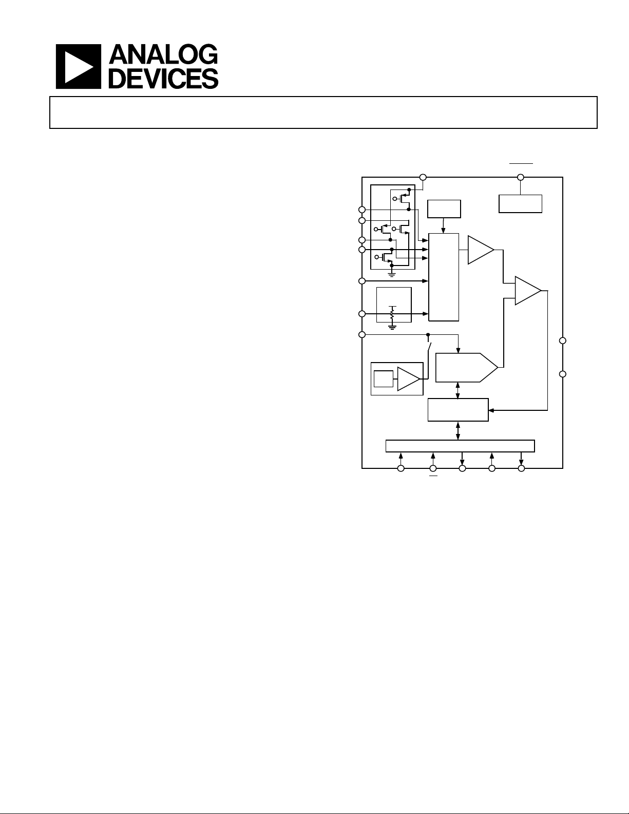
GENERAL DESCRIPTION
of 2.2 V to 5.25 V
CC
AUX
BAT
REF
AD7873
FUNCTIONAL BLOCK DIAGRAM
+V
CC
X+
X–
Y+
Y–
BATTERY
MONITOR
2.5V
BUF
REF
TEMP
SENSOR
6-TO-1
I/P
MUX
REDISTRIBUTION
CONTROL LOGIC
T/H
CHARGE
DAC
SAR + ADC
PENIRQ
PEN
INTERRUPT
AD7873
COMP
GND
+V
CC
The AD7873 is a 12-bit successive approximation ADC with a
synchronous serial interface and low on resistance switches for
driving touch screens. The AD7873 operates from a single 2.2 V
to 5.25 V power supply and features throughput rates greater
than 125 kSPS.
The AD7873 features direct battery measurement, temperature
measurement, and touch-pressure measurement. The AD7873
also has an on-board reference of 2.5 V that can be used for the
auxiliary input, battery monitor, and temperature measurement
modes. When not in use, the internal reference can be shut
down to conserve power. An external reference can also be
applied and can be varied from 1 V to V
input range is from 0 V to V
. The device includes a shutdown
REF
, while the analog
CC
mode that reduces the current consumption to less than 1 µA.
The AD7873 features on-board switches. This, coupled with low
power and high speed operation, makes the device ideal for
battery-powered systems such as personal digital assistants with
resistive touch screens and other portable equipment. The part
is available in a 16-lead 0.15" quarter size outline package
(QSOP), a 16-lead thin shrink small outline package (TSSOP),
and a 16-lead lead frame chip scale package (LFCSP).
Rev. D
Information furnished by Analog Devices is believed to be accurate and reliable.
However, no responsibility is assumed by Analog Devices for its use, nor for any
infringements of patents or other rights of third parties that may result from its use.
Specifications subject to change without notice. No license is granted by implication
or otherwise under any patent or patent rights of Analog Devices. Trademarks and
registered trademarks are the property of their respective owners.
SPORT
DIN CS DOUT DCLK BUSY
Figure 1.
PRODUCT HIGHLIGHTS
1. Ratiometric conversion mode available, eliminating errors
due to on-board switch resistances.
2. On-board temperature sensor: −40°C to +85°C.
3. Battery monitor input.
4. Touch-pressure measurement capability.
5. Low power consumption of 1.37 mW max with the
reference off, or 2.41 mW typ with the reference on, at
125 kSPS and V
6. Package options include 4 mm × 4 mm LFCSP.
7. Analog input range from 0 V to V
8. Vers ati l e s e ri a l I / O p o rt s .
One Technology Way, P.O. Box 9106, Norwood, MA 02062-9106, U.S.A.
Tel: 781.329.4700
Fax: 781.326.8703 © 2004 Analog Devices, Inc. All rights reserved.
at 3.6 V.
CC
.
REF
www.analog.com
02164-D-001
Page 2

AD7873
TABLE OF CONTENTS
Specifications..................................................................................... 3
Analog Input............................................................................... 14
Timing Specifications .................................................................. 5
Absolute Maximum Ratings............................................................ 6
ESD Caution.................................................................................. 6
Pin Configurations and Function Descriptions ........................... 7
Te r m in o l o g y ...................................................................................... 8
Typical Performance Characteristics ............................................. 9
Circuit Information........................................................................ 13
ADC Transfer Function............................................................. 13
Typical C o n necti on D i a g ram ................................................... 13
REVISION HISTORY
6/04—Changed from Rev. C to Rev. D
Updated Format..................................................................Universal
Changes to Absolute Maximum Ratings ....................................... 6
Additions to PD0 and PD1 Description...................................... 21
PBC Guidelines for Chip Scale Package Added ......................... 23
Additions to Ordering Guide........................................................ 25
4/03—Changed from Rev. B to Rev. C
Changes to Formatting ......................................................Universal
Updated Outline Dimensions....................................................... 19
Measurements............................................................................. 16
Pen Interrupt Request ................................................................ 18
Control Register ......................................................................... 19
Power vs. Throughput Rate ....................................................... 20
Serial Interface............................................................................ 21
Grounding and Layout .................................................................. 23
PCB Design Guidelines for Chip Scale Package .................... 23
Outline Dimensions....................................................................... 24
Ordering Guide .......................................................................... 25
1/02—Changed from Rev. A to Rev. B
Addition of 16-Lead Lead Frame Chip Scale Package ..Universal
Edits to Features.................................................................................1
Edits to General Description ...........................................................1
Addition of LFCSP Pin Configuration...........................................4
Edit to Absolute Maximum Ratings................................................4
Addition to Ordering Guide ............................................................4
Addition of CP-16 Outline Dimensions ..................................... 19
2/01—Changed from Rev. 0 to Rev A
Edits to Notes in the Ordering Guide
Rev. D | Page 2 of 28
Page 3

AD7873
SPECIFICATIONS
VCC = 2.7 V to 3.6 V, V
Table 1.
Parameter AD7873A1AD7873B1 Unit Test Conditions/Comments
DC ACCURACY
Resolution 12 12 Bits
No Missing Codes 11 12 Bits min
Integral Nonlinearity
Differential Nonlinearity
Offset Error
Gain Error
2
2
Noise 70 70 µV rms typ
Power Supply Rejection 70 70 dB typ
SWITCH DRIVERS
On Resistance
2
Y+, X+ 5 5 Ω typ
Y–, X– 6 6 Ω typ
ANALOG INPUT
Input Voltage Ranges 0 to V
DC Leakage Current ±0.1 ±0.1 µA typ
Input Capacitance 37 37 pF typ
REFERENCE INPUT/OUTPUT
Internal Reference Voltage 2.45/2.55 2.45/2.55 V min/max
Internal Reference Tempco ± 15 ± 15 ppm/°C typ
V
Input Voltage Range 1/VCC 1/VCC V min/max
REF
DC Leakage Current ±1 ± 1 µA max
V
Input Impedance 1 1 GΩ typ
REF
TEMPERATURE MEASUREMENT
Temperature Range –40/+85 –40/+85 °C min/max
Resolution
Differential Method
Single Conversion Method
Accuracy
Differential Method
Single Conversion Method
BATTERY MONITOR
Input Voltage Range 0/6 0/6 V min/max
Input Impedance 10 10 kΩ typ Sampling; 1 GΩ when battery monitor off
Accuracy ± 2.5 ± 2 % max External reference
± 3 ± 3 % max Internal reference
LOGIC INPUTS
Input High Voltage, V
Input Low Voltage, V
Input Current, IIN ±1 ±1 µA max Typically 10 nA, VIN = 0 V or +V
Input Capacitance, C
Footnotes on next page.
= 2.5 V internal or external, f
REF
2
2
±2 ± 1 LSB max
–0.9/+1.5 LSB max
= 2 MHz; TA = −40°C to +85°C, unless otherwise noted.
DCLK
±6 ±6 LSB max +VCC = 2.7 V
±4 ±4 LSB max External reference
0 to V
REF
3
4
3
4
2.4 2.4 V min
INH
0.4 0.4 V max
INL
5
IN
1.6 1.6 °C typ
0.3 0.3 °C typ
±2 ±2 °C typ
±2 ±2 °C typ
10 10 pF max
Volts
REF
CS = GND or +VCC; typically 260 Ω when onboard reference enabled
CC
Rev. D | Page 3 of 28
Page 4

AD7873
Parameter AD7873A1AD7873B1 Unit Test Conditions/Comments
LOGIC OUTPUTS
Output High Voltage, VOH VCC – 0.2 VCC – 0.2 V min I
Output Low Voltage, V
OL
PENIRQ Output Low Voltage, VOL
0.4 0.4 V max I
0.4 0.4 V max 100 kΩ pull-up; I
Floating-State Leakage Current ±10 ±10 µA max
Floating-State Output Capacitance510 10 pF max
Output Coding Straight (Natural) Binary
CONVERSION RATE
Conversion Time 12 12 DCLK cycles max
Track-and-Hold Acquisition Time 3 3 DCLK cycles min
Throughput Rate 125 125 kSPS max
POWER REQUIREMENTS
+VCC (Specified Performance) 2.7/3.6 2.7/3.6 V min/max Functional from 2.2 V to 5.25 V
6
I
CC
Normal Mode (f
= 125 kSPS) 380 380 µA max Internal reference off. VCC = 3.6 V,
SAMPLE
Digital I/Ps = 0 V or VCC
240 µA typ
670 670 µA typ Internal reference on. VCC = 3.6 V
Normal Mode (f
= 12.5 kSPS) 170 170 µA typ Internal reference off. VCC = 2.7 V,
SAMPLE
f
Normal Mode (Static) 150 150 µA typ Internal reference off. VCC = 3.6 V
580 580 µA typ Internal reference on. VCC = 3.6 V
Shutdown Mode (Static) 1 1 µA max 200 nA typ
Power Dissipation
Normal Mode (f
6
= 125 kSPS) 1.368 1.368 mW max VCC = 3.6 V. Internal reference disabled
SAMPLE
2.412 2.412 mW typ VCC = 3.6 V. Internal reference enabled
Shutdown 3.6 3.6 µW max VCC = 3.6 V
1
Temperature range as follows: A, B Versions: –40°C to +85°C.
2
See the section. Terminology
3
Difference between Temp0 and Temp1 measurement. No calibration necessary.
4
Temperature Drift is –2.1 mV/°C.
5
Sample tested @ 25°C to ensure compliance.
6
See the Power vs. Throughput Rate section.
= 250 µA; V
SOURCE
= 250 µA
SINK
= 200 kHz
DCLK
= 2.2 V to 5.25 V
CC
= 250 µA
SINK
Rev. D | Page 4 of 28
Page 5
AD7873
TIMING SPECIFICATIONS
TA = T
Table 2. Timing Specifications
Parameter Limit at T
f
DCLK
2 MHz max
t
ACQ
t1 10 ns min
t2 60 ns max
3
t
3
t4 200 ns min DCLK high pulse width
t5 200 ns min DCLK low pulse width
t6 60 ns max DCLK falling edge to BUSY rising edge
t7 10 ns min Data setup time prior to DCLK rising edge
t8 10 ns min Data valid to DCLK hold time
3
t
200 ns max Data access time after DCLK falling edge
9
t10 0 ns min
t11 100 ns max
t
12
1
Sample tested at 25°C to ensure compliance. All input signals are specified with tr = tf = 5 ns (10% to 90% of VCC) and timed from a voltage level of 1.6 V.
2
Mark/Space ratio for the DCLK input is 40/60 to 60/40.
3
Measured with the load circuit of and defined as the time required for the output to cross 0.4 V or 2.0 V. Figure 2
4
t12 is derived from the measured time taken by the data outputs to change 0.5 V when loaded with the circuit of . The measured number is then extrapolated
back to remove the effects of charging or discharging the 50 pF capacitor. This means that the time, t
time of the part and is independent of the bus loading.
to T
MIN
2
, unless other wise noted; VCC = 2.7 V to 5.25 V, V
MAX
1
, T
MIN
Unit Description
MAX
10 kHz min
= 2.5 V.
REF
1.5 µs min Acquisition time
CS falling edge to first DCLK rising edge
CS falling edge to busy three-state disabled
60 ns max
CS falling edge to DOUT three-state disabled
CS rising edge to DCLK ignored
CS rising edge to BUSY high impedance
4
100 ns max
CS rising edge to DOUT high impedance
, quoted in the timing characteristics is the true bus relinquish
12
Figure 2
I
OL
1.6V
I
OH
02164-D-002
TO
OUTPUT
PIN
50pF
200µA
C
L
200µA
Figure 2. Load Circuit for Digital Output Timing Specifications
Rev. D | Page 5 of 28
Page 6
AD7873
ABSOLUTE MAXIMUM RATINGS
TA = 25°C, unless otherwise noted.
Table 3.
Parameter Rating
+VCC to GND –0.3 V to +7 V
Analog Input Voltage to GND –0.3 V to VCC + 0.3 V
Digital Input Voltage to GND –0.3 V to VCC + 0.3 V
Digital Output Voltage to GND –0.3 V to VCC + 0.3 V
V
to GND –0.3 V to VCC + 0.3 V
REF
Input Current to Any Pin Except Supplies1 ±10 mA
Operating Temperature Range
Commercial (A, B Versions) –40°C to +85°C
Storage Temperature Range –65°C to +150°C
Junction Temperature 150°C
QSOP, TSSOP, LFCSP Packages, Power
Dissipation
θJA Thermal Impedance 149.97°C/W (QSOP)
150.4°C/W (TSSOP)
135.7°C/W (LFCSP)
θJC Thermal Impedance 38.8°C/W (QSOP)
27.6°C/W (TSSOP)
IR Reflow Soldering
Peak Temperature
Time-to-Peak Temperature
Ramp-Down Rate
Pb-free Parts Only:
Peak Temperture 250°C
Time-to-Peak Temperature
Ramp-Up Rate
Ramp-Down Rate
450 mW
220°C (±5°C)
10 sec to 30 sec
6°C/sec max
20 sec to 40 sec
3°C/sec max
6°C/sec max
___________________________
1
Transient currents of up to 100 mA do not cause SCR latch-up.
Stresses above those listed under Absolute Maximum Ratings
may cause permanent damage to the device. This is a stress
rating only; functional operation of the device at these or any
other conditions above those listed in the operational sections
of this specification is not implied. Exposure to absolute
maximum rating conditions for extended periods may affect
device reliability.
ESD CAUTION
ESD (electrostatic discharge) sensitive device. Electrostatic charges as high as 4000 V readily accumulate on the
human body and test equipment and can discharge without detection. Although this product features
proprietary ESD protection circuitry, permanent damage may occur on devices subjected to high energy
electrostatic discharges. Therefore, proper ESD precautions are recommended to avoid performance
degradation or loss of functionality.
Rev. D | Page 6 of 28
Page 7
AD7873
PIN CONFIGURATIONS AND FUNCTION DESCRIPTIONS
BAT
V
GNDY–X–
16 15 14 13
1
2
3
4
(Not to Scale)
PIN 1
INDICATOR
AD7873
TOP VIEW
5678
DIN
BUSY
DOUT
CS
AUX
V
REF
+V
PENIRQ
CC
Figure 3. LFCSP Pin Configuration
1
+V
CC
2
X+
3
GND
V
AUX
Y+
X–
Y–
BAT
AD7873
4
TOP VIEW
5
(Not to Scale)
6
7
8
12
Y+
11
X+
+V
10
CC
9
DCLK
02164-D-003
Figure 4.QSOP/TSSOP Pin Configuration
16
15
14
13
12
11
10
9
DCLK
CS
DIN
BUSY
DOUT
PENIRQ
+V
CC
V
REF
02164-D-004
Table 4. Pin Function Descriptions
Mnemonic Function
+VCC
Power Supply Input. The +V
range for the AD7873 is from 2.2 V to 5.25 V. Both +VCC pins should be connected directly
CC
together.
X+ X+ Position Input. ADC Input Channel 1.
Y+ Y+ Position Input. ADC Input Channel 2.
X– X– Position Input.
Y– Y– Position Input. ADC Input Channel 3.
GND
Analog Ground. Ground reference point for all circuitry on the AD7873. All analog input signals and any external reference
signals should be referred to this GND voltage.
V
BAT
Battery Monitor Input. ADC Input Channel 4.
AUX Auxiliary Input. ADC Input Channel 5.
V
REF
Reference Output for the AD7873. Alternatively an external reference can be applied to this input. The voltage range for the
external reference is 1.0 V to +V
. For specified performance, it is 2.5 V on the AD7873. The internal 2.5 V reference is
CC
available on this pin for use external to the device. The reference output must be buffered before it is applied elsewhere in a
system. A 0.1 µF capacitor is recommended between this pin and GND to reduce system noise effects.
PENIRQ
DOUT
BUSY
DIN
Pen Interrupt. CMOS logic open drain output (requires 10 kΩ to 100 kΩ pull-up resistor externally).
Data Out. Logic Output. The conversion result from the AD7873 is provided on this output as a serial data stream. The bits are
clocked out on the falling edge of the DCLK input. This output is high impedance when
BUSY Output. Logic Output. This output is high impedance when
CS is high.
CS is high.
Data In. Logic Input. Data to be written to the AD7873 control register is provided on this input and is clocked into the
register on the rising edge of DCLK (see the Control Register section).
CS Chip Select Input. Active Low Logic Input. This input provides the dual function of initiating conversions on the AD7873 and
enabling the serial input/output register.
DCLK
External Clock Input. Logic Input. DCLK provides the serial clock for accessing data from the part. This clock input is also used
as the clock source for the AD7873 conversion process.
Rev. D | Page 7 of 28
Page 8

AD7873
TERMINOLOGY
Integral Nonlinearity
This is the maximum deviation from a straight line passing
through the endpoints of the ADC transfer function. The
endpoints of the transfer function are zero scale, a point 1 LSB
below the first code transition, and full scale, a point 1 LSB
above the last code transition.
Differential Nonlinearity
This is the difference between the measured and the ideal 1 LSB
change between any two adjacent codes in the ADC.
Offset Error
This is the deviation of the first code transition (00 . . . 000) to
(00 . . . 001) f rom the ideal, that is, AGND + 1 LSB.
Gain Error
This is the deviation of the last code transition (111 . . . 110) to
(111 . . . 111) from the ideal (that is, V
error is adjusted out.
Track-and-Hold Acquisition Time
The track-and-hold amplifier enters the acquisition phase on
the fifth falling edge of DCLK after the START bit has been
detected. Three DCLK cycles are allowed for the track-and-hold
acquisition time. The input signal is fully acquired to the 12-bit
level within this time even with the maximum specified DCLK
frequency. See the Analog Input section for more details.
On-Resistance
This is a measure of the ohmic resistance between the drain and
source of the switch drivers.
– 1 LSB) after the offset
REF
Rev. D | Page 8 of 28
Page 9
AD7873
TYPICAL PERFORMANCE CHARACTERISTICS
207
206
205
204
203
202
201
SUPPLY CURRENT (µA)
200
199
198
–40 –20 0 20 40 60 80 100
TEMPERATURE (°C)
Figure 5. Supply Current vs. Temperature
230
f
220
210
SAMPLE
V
REF
= 12.5kHz
= +V
CC
02164-D-005
141
140
139
138
137
136
SUPPLY CURRENT (nA)
135
134
–40 –20 0 20 40 60 80 100
TEMPERATURE (°C)
Figure 8. Power-Down Supply Current vs. Temperature
1000
02164-D-008
200
190
180
SUPPLY CURRENT (µA)
170
160
150
2.2 2.6 3.0 3.4 3.8 4.2 4.6 5.0
+V
(V)
CC
Figure 6. Supply Current vs. +V
CC
0.20
0.15
0.10
0.05
0
–0.05
DELTA FROM 25°C (LSB)
–0.10
–0.15
02164-D-006
SAMPLE RATE (kSPS)
100
0.6
0.4
0.2
0
–0.2
DELTA FROM 25°C (LSB)
–0.4
V
REF
3.2 3.72.2 2.7 4.2 4.7 5.2
+V
(V)
CC
Figure 9. Maximum Sample Rate vs. +V
= +V
CC
CC
02164-D-009
–0.20
–40 –20 0 20 40 60 80 100
TEMPERATURE (°C)
Figure 7. Change in Gain vs. Temperature
02164-D-007
Rev. D | Page 9 of 28
–0.6
–40 –20 0 20 40 60 80 100
TEMPERATURE (°C)
Figure 10. Change in Offset vs. Temperature
02164-D-010
Page 10

AD7873
7.5
6.5
5.5
4.5
3.5
2.5
REFERENCE CURRENT (µA)
1.5
0.5
10
705525 4010 85 100 115 130
SAMPLE RATE (kHz)
Figure 11. Reference Current vs. Sample Rate
02164-D-011
14
13
12
11
10
9
8
7
6
5
REFERENCE CURRENT (µA)
4
3
2
020–40 –20 40 60 80
TEMPERATURE (°C)
02164-D-014
Figure 14. Reference Current vs. Temperature
9
9
Y+
X+
8
(Ω)
7
ON
R
6
5
4
2.0 2.5 3.0 3.5 4.0 4.5 5.0 5.5
X–
Y–
+V
(V)
CC
Figure 12. Switch On Resistance vs. +V
(X+, Y+: +V
to Pin; X-, Y-: Pin to GND)
CC
2.0
1.8
1.6
1.4
1.2
1.0
0.8
ERROR (LSB)
0.6
0.4
0.2
0
15 35 55 75 95 115 135 155 175 195
INL: R = 500Ω
DNL: R = 2kΩ
DNL: R = 500Ω
SAMPLING RATE (kSPS)
INL: R = 2kΩ
8
7
(Ω)
6
ON
R
5
4
3
–40 –20 0 20 40 60 80 100
02164-D-012
CC
Figure 15. Switch On Resistance vs. Temperature
Y–
Y+
TEMPERATURE (°C)
X+
X–
02164-D-015
(X+, Y+: +VCC to Pin; X-, Y-: Pin to GND)
2.5006
2.5004
2.5002
2.5000
(V)
REF
2.4998
2.4996
2.4994
INTERNAL V
2.4992
2.4990
2.4988
–40 –30 –20 –10 0 10 20 30 40 50 60 70 80
02164-D-013
TEMPERATURE (°C)
02164-D-016
Figure 13. Maximum Sampling Rate vs. R
IN
Figure 16. Internal V
vs. Temperature
REF
Rev. D | Page 10 of 28
Page 11

AD7873
2.504
2.502
2.500
2.498
2.496
(V)
2.494
REF
V
2.492
2.490
2.488
2.486
2.484
2.9 3.12.5 2.7 3.3 3.5 3.7
+V
(V)
CC
Figure 17. Internal V
REF
vs. +V
CC
850
800
95.95mV
750
700
650
600
550
TEMP DIODE VOLTAGE (mV)
500
450
–40 –30 –20 –10 0 10 20 30 40 50 60 70 80
TEMP1
TEMP0
TEMPERATURE (°C)
Figure 18. Temp Diode Voltage vs. Temperature (2.7 V Supply)
730
729
728
727
726
725
724
723
TEMP1 DIODE VOLTAGE (mV)
722
721
720
2.7 3.33.0 3.6
V
(V)
SUPPLY
142.15mV
02164-D-017
02164-D-018
02164-D-019
5
4
(V)
3
REF
NO CAP (7µS)
2
SETTLING TIME
INTERNAL V
1
0
0 200 400 600 800 1000 1200 1400 1600 1800
Figure 20. Internal V
1µF CAP (1800µS)
SETTLING TIME
TURN-ON TIME (µS)
vs. Turn-on Time
REF
610
609
608
607
606
605
604
603
TEMP0 DIODE VOLTAGE (mV)
602
601
600
2.7 2.8 2.9 3.0 3.1 3.2 3.3 3.4 3.5 3.6
V
(V)
SUPPLY
Figure 21. Temp0 Diode Voltage vs. V
SUPPLY
0
f
= 125kHz
SAMPLE
f
= 15kHz
20
40
60
SNR (dB)
80
100
120
30.022.57.5 15.00 37.5 45.0 52.5 60.0
FREQUENCY (kHz)
IN
SNR = 68.34dB
02164-D-020
02164-D-021
(25°C)
02164-D-022
Figure 19. Temp 1 Diode Voltage vs. V
SUPPLY
(25°C)
Rev. D | Page 11 of 28
Figure 22. Auxiliary Channel Dynamic Performance
( f
SAMPLE
=125 kHz, f
= 15 kHz)
INPUT
Page 12

AD7873
0
VCC = 3V
100mV p-p SINEWAVE ON +V
–20
V
REF
f
SAMPLE
–40
= 2.5V EXT REFERENCE
= 125kHz,
f
= 20kHz
IN
Figure 23 shows the power supply rejection ratio versus V
CC
supply frequency for the AD7873. The power supply rejection
DD
ratio is defined as the ratio of the power in the ADC output at
full-scale frequency, f, to the power of a 100 mV sine wave
applied to the ADC V
supply of frequency fS:
CC
–60
PSRR (dB)
–80
–100
–120
0 102030405060708090100
RIPPLE FREQUENCY (kHz)
V
CC
Figure 23. AC PSRR vs. Supply Ripple Frequency
02164-D-023
PSSR (dB) = 10 log (Pf/Pfs)
where:
Pf is power at frequency, f, in ADC output.
Pfs is power at frequency, f
Here a 100 mV p-p sine wave is coupled onto the V
, coupled onto t he ADC VCC supply.
S
supply.
CC
Decoupling capacitors of 10 µF and 0.1 µF were used on the
supply.
Rev. D | Page 12 of 28
Page 13

AD7873
CIRCUIT INFORMATION
The AD7873 is a fast, low-power, 12-bit, single-supply A/D
converter. The AD7873 can be operated from a 2.2 V to 5.25 V
supply. When operated from either a 5 V supply or a 3 V supply,
the AD7873 is capable of throughput rates of 125 kSPS when
provided with a 2 MHz clock.
The AD7873 provides the user with an on-chip track-and-hold,
multiplexer, A/D converter, reference, temperature sensor, and
serial interface housed in a tiny 16-lead QSOP, TSSOP, or
LFCSP package, which offers the user considerable space-saving
advantages over alternative solutions. The serial clock input
(DCLK) accesses data from the part and also provides the clock
source for the successive approximation ADC. The analog input
range is 0 V to V
REF
between 1 V and +V
(where the externally applied V
). The AD7873 has a 2.5 V reference on
CC
can be
REF
board with this reference voltage available for use externally if
buffered.
The analog input to the ADC is provided via an on-chip
multiplexer. This analog input can be any one of the X, Y, and Z
panel coordinates, battery voltage, or chip temperature. The
multiplexer is configured with low-resistance switches that
allow an unselected ADC input channel to provide power and
an accompanying pin to provide ground for an external device.
For some measurements, the on-resistance of the switches could
present a source of error. However, with a differential input to
the converter and a differential reference architecture, this error
can be negated.
ADC TRANSFER FUNCTION
The output coding of the AD7873 is straight binary. The
designed code transitions occur at successive integer LSB values
(that is, 1 LSB, 2 LSBs, and so on). The LSB size is V
REF
/4096.
The ideal transfer characteristic for the AD7873 is shown in
Figure 24.
111...111
111...110
111...000
011...111
ADC CODE
000...010
000...001
000...000
1LSB
0V
ANALOG INPUT
Figure 24. Transfer Characteristic
1LSB = V
/4096
REF
+V
–1LSB
REF
02164-D-024
TYPICAL CONNECTION DIAGRAM
Figure 25 shows a typical connection diagram for the AD7873
in a touch screen control application. The AD7873 features an
internal reference, but this can be overdriven with an external
low impedance source between 1 V and +V
reference voltage sets the input range of the converter. The
conversion result is output MSB first, followed by the remaining
11 bits and three trailing zeroes, depending on the number of
clocks used per conversion. (See the Serial Interface section.)
For applications where power consumption is a concern, the
power management option should be used to improve power
performance. See Table 7 for available power management
options.
. The value of the
CC
2.2V TO 5V
TOUCH
SCREEN
1µF TO 10µF
(OPTIONAL)
TO BATTERY
VOLTAGE
REGULATOR
AUXILIARY
INPUT
0.1µF
1
2
3
4
5
6
7
8
+V
CC
X+
AD7873
Y+
X–
Y–
GND
V
BAT
AUX
DCLK
CS
DIN
BUSY
DOUT
PENIRQ
+V
V
REF
16
15
14
13
12
11
10
CC
9
0.1µF
SERIAL/CONVERSION CLOCK
CHIP SELECT
SERIAL DATA IN
CONVERTER STATUS
SERIAL DATA OUT
PEN INTERRUPT
50kΩ
02164-D-025
Figure 25. Typical Application Circuit
Rev. D | Page 13 of 28
Page 14

AD7873
ANALOG INPUT
Figure 26 shows an equivalent circuit of the analog input
structure of the AD7873, which contains a block diagram of the
input multiplexer, the differential input of the ADC, and the
differential reference.
Table 5 shows the multiplexer address corresponding to each
analog input, both for the SER/
set high and low. The control bits are provided serially to the
device via the DIN pin. For more information on the control
register, see the Control Register section.
When the converter enters hold mode, the voltage difference
between the +IN and –IN inputs (see Figure 26) is captured on
the internal capacitor array. The input current on the analog
inputs depends on the conversion rate of the device. During the
sample period, the source must charge the internal sampling
capacitor (typically 37 pF). Once the capacitor is fully charged,
there is no further input current. The rate of charge transfer
from the analog source to the converter is a function of
conversion rate.
bit in the control register
DFR
V
BAT
AUX
TEMP
X+
Y+
Y–
V
CC
X+
X–
Y+
Y–
ON-CHIP SWITCHES
IN+
6-TO-1
MUX
IN+
Figure 26. Equivalent Analog Input Circuit
REF
INT/
X+ Y+
EXT
3-TO-1
MUX
REF+
ADC CORE DATA OUT
IN– REF–
3-TO-1
MUX
X– Y– GND
02164-D-026
Table 5. Analog Input, Reference, and Touch Screen Control
A2 A1 A0
SER/
DFR
Analog Input X Switches Y Switches +REF
0 0 0 1 TEMP0 OFF OFF V
0 0 1 1 X+ OFF ON V
0 1 0 1 VBAT OFF OFF V
0 1 1 1 X+ (Z1) X+ OFF Y+ ON V
1
–REF1
GND
REF
GND
REF
REF
REF
GND
GND
X– ON Y– OFF
1 0 0 1 Y– (Z2) X+ OFF Y+ ON V
GND
REF
X– ON Y– OFF
1 0 1 1 Y+ ON OFF V
1 1 0 1 AUX OFF OFF V
1 1 1 1 TEMP1 OFF OFF V
0 0 0 0
Invalid Address. Test Mode: Switches out the Temp0 diode to the
GND
REF
REF
GND
REF
PENIRQ
pin.
GND
0 0 1 0 X+ OFF ON Y+ Y–
0 1 0 0
Invalid Address
0 1 1 0 X+ (Z1) X+ OFF Y+ ON Y+ X–
X– ON Y– OFF
1 0 0 0 Y– (Z2) X+ OFF Y+ ON Y+ X–
X– ON Y– OFF
1 0 1 0 Y+ ON OFF X+ X–
1 1 0 0
1 1 1 0
Outputs Identity Code, 1000 0000 0000.
Invalid address. Test mode: Switches out the Temp1 diode to the
PENIRQ
pin.
1
Internal node, not directly accessible by the user.
Rev. D | Page 14 of 28
Page 15

AD7873
Acquisition Time
The track-and-hold amplifier enters tracking mode on the
falling edge of the fifth DCLK after the START bit is detected
(see Figure 35). The time required for the track-and-hold
amplifier to acquire an input signal depends on how quickly the
37 pF input capacitance is charged. With zero source impedance
on the analog input, three DCLK cycles are always sufficient to
acquire the signal to the 12-bit level. With a source impedance
on the analog input, the actual acquisition time required is
R
IN
calculated using the formula:
where R
()
Rt
INACQ
is the source impedance of the input signal, and 100 Ω,
IN
pF371004.8 ×Ω+×=
37 pF is the input RC. Depending on the frequency of DCLK
used, three DCLK cycles may or may not be sufficient to acquire
the analog input signal with various source impedance values.
Touch Screen Settling
In some applications, external capacitors could be required
across the touch screen to filter noise associated with it, for
example, noise generated by the LCD panel or backlight
circuitry. The value of these capacitors causes a settling time
requirement when the panel is touched. The settling time
typically appears as a gain error. There are several methods for
minimizing or eliminating this issue. The problem may be that
the input signal, reference, or both, have not settled to their final
value before the sampling instant of the ADC. Additionally, the
reference voltage could still be changing during the conversion
cycle. One option is to stop or slow down the DCLK for the
required touch screen settling time. This allows the input and
reference to stabilize for the acquisition time, which resolves the
issue for both single-ended and differential modes.
The other option is to operate the AD7873 in differential mode
only for the touch screen, and program the AD7873 to keep the
touch screen drivers on and not go into power-down (PD0 =
PD1 = 1). Several conversions could be required, depending on
the settling time required and the AD7873 data rate. Once the
required number of conversions have been made, the AD7873
can then be placed in a power-down state on the last measurement. The last method is to use the 15 DCLK cycle mode, which
maintains the touch screen drivers on until it is commanded by
the processor to stop.
Internal Reference
The AD7873 has an internal reference voltage of 2.5 V. The
internal reference is available on the V
pin for external use in
REF
the system; however, it must be buffered before it is applied
elsewhere. The on-chip reference can be turned on or off with
the power-down address, PD1 = 1 (see Table 7 and Figure 27).
Typically the reference voltage is only used in single-ended
mode for battery monitoring, temperature measurement, and
for using the auxiliary input. Optimal touch screen performance
is achieved when using the differential mode. The power-up
time of the 2.5 V reference is typically 10 µs without a load;
however, a 0.1 µF capacitor on the V
pin is recommended for
REF
optimum performance, which affects the power-up time. (See
Figure 20.)
X+
Y+
V
REF
SW1
Figure 27. On-Chip Reference Circuitry
2.5V
REF
260Ω
3-TO-1
MUX
BUF
ADC
02164-D-027
Reference Input
The voltage difference between +REF and −REF (see Figure 26)
sets the analog input range. The AD7873 operates with a reference input in the range of 1 V to +V
. Figure 27 shows the on-
CC
chip reference circuitry on the AD7873. The internal reference
on the AD7873 can be overdriven with an external reference;
for best performance, however, the internal reference should be
disabled when an external reference is applied, because SW1 in
Figure 27 opens on the AD7873 when the internal reference is
disabled. The on-chip reference always is available at the V
REF
pin as long as the reference is enabled. The input impedance
seen at the V
pin is approximately 260 Ω when the internal
REF
reference is enabled. When it is disabled, the input impedance
seen at the V
pin is in the gigaOhm region.
REF
When making touch screen measurements, conversions can be
made in differential (ratiometric) mode or single-ended mode.
If the SER/
bit is set to 1 in the control register, then a
DFR
single-ended conversion is performed. Figure 28 shows the
configuration for a single-ended Y coordinate measurement.
The X+ input is connected to the analog-to-digital converter,
the Y+ and Y− drivers are turned on, and the voltage on X+ is
digitized. The conversion is performed with the ADC referenced
from GND to V
. This V
REF
the voltage applied at the V
is either the on-chip reference or
REF
pin externally, and is determined
REF
by the setting of the power management Bits PD0 and PD1 (see
Table 6). The advantage of this mode is that the switches that
Rev. D | Page 15 of 28
Page 16

AD7873
(
(
)
×=∆
κ
(
(
)
×=∆
κ
supply the external touch screen can be turned off once the
acquisition is complete, resulting in a power savings. However,
the on-resistance of the Y drivers affects the input voltage that
can be acquired. The full touch screen resistance could be in the
order of 200 Ω to 900 Ω, depending on the manufacturer. Thus,
if the on-resistance of the switches is approximately 6 Ω, true
full-scale and zero-scale voltages cannot be acquired, regardless
of where the pen/stylus is on the touch screen. Note that the
minimum touch screen resistance recommended for use with
the AD7873 is approximately 70 Ω. In this mode of operation,
therefore, some voltage is likely to be lost across the internal
switches, and it is unlikely that the internal switch resistance
will track the resistance of the touch screen over temperature
and supply, providing an additional source of error.
+V
CC
Y+
X+ IN+
Y–
IN+
ADC CORE
IN–
V
REF
REF+
REF–
MEASUREMENTS
Temperature Measurement
Two temperature measurement options are available on the
AD7873, the single conversion method and the differential
conversion method. Both methods are based on an on-chip
diode measurement.
In the single conversion method, a diode voltage is digitized and
recorded at a fixed calibration temperature. Any subsequent
polling of the diode provides an estimate of the ambient temperature through extrapolation from the calibration temperature
diode result. This assumes a diode temperature drift of
approximately –2.1 mV/°C. This method provides a resolution
of approximately 0.3°C and a predicted accuracy of ±3°C.
The differential conversion method is a 2-point measurement.
The first measurement is performed with a fixed bias current
into a diode, and the second measurement is performed with a
fixed multiple of the bias current into the same diode. The
voltage difference in the diode readings is proportional to
absolute temperature and is given by the following formula:
)
BE
/
NlnqTV
GND
Figure 28. Single-Ended Reference Mode (SER/
The alternative to this situation is to set the SER/
DFR
DFR
02164-D-028
= 1)
bit low.
Again, making a Y coordinate measurement is considered, but
now the +REF and –REF nodes of the ADC are connected
directly to the Y+ and Y– pins. This means the analog-to-digital
conversion is ratiometric. The result of the conversion is always
a percentage of the external resistance, independent of how it
could change with respect to the on resistance of the internal
switches. Figure 29 shows the configuration for a ratiometric Y
coordinate measurement.
+V
CC
Y+
X+ IN+
Y–
GND
Figure 29. Differential Reference Mode (SER/
IN+
ADC CORE
IN–
REF+
REF–
DFR
02164-D-029
= 0)
where V
represents the diode voltage, N is the bias current
BE
multiple, k is Boltzmann’s constant and q is the electron charge.
This method provides more accurate absolute temperature
measurement of ± 2°C. However, the resolution is reduced to
approximately 1.6°C. Assuming a current multiple of 105
(which is typical for the AD7873) taking Boltzmann’s constant,
k = 1.38054 ×10
charge q = 1.602189 × 10
–23
electrons volts/degrees Kelvin, the electron
–19
, then T, the ambient temperature in
degrees centigrade, would be calculated as follows:
)
BE
()
∆V
is calculated from the difference in readings from the first
BE
/
BE
NlnqTV
()
NlnqVT
/
××∆=
κ
3
BE
ΚVCT
2731049.2
−∆××=°
conversion and second conversion.
Figure 30 shows a block diagram of the temperature
measurement mode.
TEMP0 TEMP1
I
105*I
MUX
ADC
The disadvantage of this mode of operation is that during both
the acquisition phase and conversion process, the external touch
screen must remain powered. This results in additional supply
current for the duration of the conversion.
Rev. D | Page 16 of 28
Figure 30. Block Diagram of Temperature Measurement Circuit
02164-D-030
Page 17

AD7873
(
(
[
−
××=
(
(
[
{
Battery Measurement
The AD7873 can monitor a battery voltage from 0 V to 6 V.
Figure 31 shows a block diagram of a battery voltage monitored
through the V
pin. The voltage to the +VCC of the AD7873 is
BAT
maintained at the desired supply voltage via the dc/dc regulator
while the input to the regulator is monitored. This voltage on
V
is divided by 4 so that a 6 V battery voltage is presented to
BAT
the ADC as 1.5 V. To conserve power, the divider is on only
during the sampling of a voltage on V
. Table 5 shows the
BAT
control bit settings required to perform a battery measurement.
DC/DC
BATTERY
0V TO 6V
+
CONVERTER
V
BAT
7.5kΩ
2.5kΩ
+V
0V TO 1.5V
CC
ADC CORE
Pressure Measurement
The pressure applied to the touch screen via a pen or finger can
also be measured with the AD7873 with some simple calculations. The 8-bit resolution mode would be sufficient for this
measurement, but the following calculations are shown with the
12-bit resolution mode. The contact resistance between the X
and Y plates is measured, which provides a good indication of
the size of the depressed area and the applied pressure. The area
of the spot touched is proportional to the size of the object
touching it. The size of this resistance (R
) can be calculated
TOUCH
using two different methods.
The first method requires the user to know the total resistance
of the X-plate tablet. Three touch screen conversions are
required, a measurement of the X-position, Z
-position, and Z2-
1
position (see Figure 32). The following equation calculates the
touch resistance:
)( )
)
1/4095/
ZZXRR
12POSITIONXPLATETOUCH
]
Figure 31. Block Diagram of Battery Measurement Circuit
+
–
X+
TOUCH TOUCH
-POSITION Z1-POSITION
Z
2
X–
Y+
+
–
Y–
MEASURE Z
Figure 32. Pressure Measurement Block Diagram
02164-D-031
X+
TOUCH
X-POSITION
X–
MEASURE Z
MEASURE X-POSITION
Y+
Y–
-POSITION
1
-POSITION
2
The second method requires that the resistance of both the
X-plate and Y-plate tablets are known. Again three touch screen
conversions are required, a measurement of the X-position,
Y-po s itio n , a n d Z
-position (see Figure 32).
1
The following equation also calculates the touch resistance:
ZXZRR
)( )
(){}
YR
×−
POSITIONYPLATE
4095/
−×=
)
1POSITION1XPLATETOUCH
X+
X–
Y+
+
–
Y–
02164-D-032
]
1/40964095//
}
Rev. D | Page 17 of 28
Page 18

AD7873
PEN INTERRUPT REQUEST
The pen interrupt equivalent circuitry is outlined in Figure 33.
By connecting a pull-up resistor (10 kΩ to 100 kΩ) between +V
and this CMOS logic open drain output, the
remains high normally. If
PENIRQ
is enabled (see Table 7), when
PENIRQ
output
the touch screen connected to the AD7873 is touched by a pen
or finger, the
PENIRQ
output goes low, initiating an interrupt to
a microprocessor, which can then instruct a control word to be
written to the AD7873 to initiate a conversion. This output can
also be enabled between conversions during power-down (see
Table 7) allowing power-up to be initiated only when the screen
is touched. The result of the first touch screen coordinate conversion after power-up is valid, assuming any external reference
is settled to the 12-bit or 8-bit level as required.
Figure 34 assumes that the
PENIRQ
the last write or that the part was just powered up so
enabled by default. Once the screen is touched, the
output goes low a time t
later. This delay is approximately
PEN
function was enabled in
PENIRQ
PENIRQ
5 µs, assuming a 10 nF touch screen capacitance, and varies with
the touch screen resistance actually used. Once the START bit is
detected, the pen interrupt function is disabled and the
cannot respond to screen touches. The
PENIRQ
PENIRQ
output remains
low until the fourth falling edge of DCLK after the START bit is
clocked in, at which point it returns high as soon as possible,
irrespective of the touch screen capacitance. This does not mean
that the pen interrupt function is now enabled again because
the power-down bits have not yet been loaded to the control
register. Regardless of whether
the
PENIRQ
PENIRQ
conversion is complete, the
screen touch. The fact that
output normally always idles high . Assuming the
is enabled again as shown in Figure 34, then once the
PENIRQ
PENIRQ
PENIRQ
is to be enabled again,
output again responds to a
returns high almost
immediately after the fourth falling edge of DCLK means the
CC
is
user avoids any spurious interrupts on the microprocessor or
DSP, which could occur if the interrupt request line on the
micro/DSP were unmasked during or toward the end of
conversion and the
PENIRQ
START bit is detected by the AD7843, the
pin was still low. Once the next
PENIRQ
function is
again disabled.
If the control register write operation overlaps with the data
read, a START bit is always detected prior to the end of
conversion, meaning that even if the
PENIRQ
function is
enabled in the control register, it is disabled by the START bit
again before the end of the conversion is reached, so the
PENIRQ
function effectively cannot be used in this mode.
However, as conversions are occurring continuously, the
PENIRQ
function is not necessary and is therefore redundant.
+V
CC
100kΩ
Y+
+V
CC
PENIRQ
EXTERNAL
PULL-UP
TOUCH
SCREEN
X+
Y–
Figure 33.
PENIRQ
ENABLE
ON
PENIRQ
Functional Block Diagram
02164-D-033
SCREEN
TOUCHED
PENIRQ
CS
DCLK
DIN
HERE
t
PEN
INTERRUPT
PROCESSOR
NO RESPONSE TO TOUCH
SER/
SA2A1A0 1 0
(START)
Figure 34.
MODE
DFR
PENIRQ
Timing Diagram
Rev. D | Page 18 of 28
PD1 = 1, PD0 = 0, PENIRQ
ENABLED AGAIN
81 1 13 16
02164-D-034
Page 19

AD7873
CONTROL REGISTER
The control word provided to the ADC via the DIN pin is
shown in Table 6. This provides the conversion start, channel
addressing, ADC conversion resolution, configuration, and
power-down of the AD7873.
provides detailed information on the order and
Tabl e 6
description of these control bits within the control word.
Initiate START
The first bit, the S bit, must always be set to 1 to initiate the start
of the control word. The AD7873 ignores any inputs on the DIN
line until the start bit is detected.
Channel Addressing
The next three bits in the control register, A2, A1, and A0, select
the active input channel(s) of the input multiplexer (see Table 5
and Figure 26), touch screen drivers, and the reference inputs.
Mode
The MODE bit sets the resolution of the analog-to-digital
converter. With a 0 in this bit, the following conversion has
12 bits of resolution. With a 1 in this bit, the following
conversion has 8 bits of resolution.
SER/
The SER/
DFR
bit controls the reference mode, which can be
DFR
either single-ended or differential if a 1 or a 0 is written to this
bit respectively. The differential mode is also referred to as the
ratiometric conversion mode. This mode is optimum for
X-position, Y-position, and pressure-touch measurements. The
reference is derived from the voltage at the switch drivers,
which is almost the same as the voltage to the touch screen. In
this case, a separate reference voltage is not needed because the
reference voltage to the ADC is the voltage across the touch
screen. In single-ended mode, the reference voltage to the
converter is always the difference between the V
pins. See Table 5 and Figure 26 through Figure 29 for further
information.
If X-position, Y-position, and pressure touch are measured in
single-ended mode, an external reference voltage or +V
required for maximum dynamic range. The internal reference
can be used for these single-ended measurements; however, a
loss in dynamic range is incurred. If an external reference is
used, the AD7873 should also be powered from the external
reference. Because the supply current required by the device is
so low, a precision reference can be used as the supply source to
the AD7873. It might also be necessary to power the touch
screen from the reference, which could require 5 mA to 10 mA.
A REF19x voltage reference can source up to 30 mA, and, as
such, could supply both the ADC and the touch screen. Care
must be taken however, to ensure that the input voltage applied
to the ADC does not exceed the reference voltage and therefore
the supply voltage. See the Absolute Maximum Ratings section.
Note that the differential mode can only be used for X-position,
Y-position, and pressure touch measurements. All other
measurements require single-ended mode.
PD0 and PD1
The power management options are selected by programming
the power management bits, PD0 and PD1, in the control
register. Table 7 summarizes the options available and the
internal reference voltage configurations. The internal reference
can be turned on or off independent of the analog-to-digital
converter, allowing power saving between conversions using the
power management options. On power-up, PD0 defaults to 0,
while PD1 defaults to 1.
and GND
REF
is
CC
Table 6. Control Register Bit Function Description
MSB
S A2 A1 A0 MODE SER/DFR PD1 PD0
LSB
Bit No. Mnemonic Comment
7 S
6–4 A2–A0
3 MODE
2
1, 0 PD1, PD0 Power Management Bits. These two bits decode the power-down mode of the AD7873 as shown in Table 7.
DFR Single-Ended/Differential Reference Select Bit. Along with Bits A2–A0, this bit controls the setting of the
SER/
Start Bit. The control word starts with the first high bit on DIN. A new control word can start every 15th DCLK cycle
when in the 12-bit conversion mode or every 11th DCLK cycle when in 8-bit conversion mode.
Channel Select Bits. These three address bits along with the SER/DFR bit control the setting of the multiplexer
input, switches, and reference inputs, as detailed in Table 5.
12-Bit/8-Bit Conversion Select Bit. This bit controls the resolution of the following conversion. With a 0 in this bit,
the conversion has 12-bit resolution or, with a 1 in this bit, 8-bit resolution.
multiplexer input, switches, and reference inputs as described in Table 5.
Rev. D | Page 19 of 28
Page 20

AD7873
Table 7. Power Management Options
PD1 PD0
PENIRQ
0 0 Enabled
0 1 Enabled
1 0 Enabled
1 1 Disabled This configuration results in always keeping the device powered up. The reference and the ADC are on.
POWER VS. THROUGHPUT RATE
By using the power-down options on the AD7873 when not
converting, the average power consumption of the device
decreases at lower throughput rates. Figure 35 shows how, as the
throughput rate is reduced while maintaining the DCLK
frequency at 2 MHz, the device remains in its power-down state
longer and the average current consumption over time drops
accordingly.
1000
f
DCLK
100
f
10
SUPPLY CURRENT (µA)
1
DCLK
0 120
Figure 35. Supply Current vs. Throughput (µA)
Description
This configuration results in immediate power-down of the on chip reference as soon as PD1 is set to 0. The ADC
powers down only between conversions. When PD0 is set to 0, the conversion is performed first and the ADC
powers down upon completion of that conversion (or upon the rising edge of
the next conversion, the ADC instantly powers up to full power. This means if the device is being used in the
differential mode, or an external reference is used, there is no need for additional delays to ensure full operation
and the very first conversion is valid. The Y– switch is on while in power-down. When the device is performing
differential table conversions, the reference and reference buffer do not attempt to power up with Bits PD1 and
PD0 programmed in this way.
This configuration results in switching the reference off immediately and the ADC on permanently. When the
device is performing differential tablet conversions, the reference and reference buffer do not attempt to power
up with bits PD1 and PD0 programmed in this way.
This configuration results in switching the reference on and powering the ADC down between conversions. The
ADC powers down only between conversions. When PD0 is set to 0, the conversion is performed first, and the
ADC powers down upon completion of the conversion (or upon the rising edge of CS if it occurs first). At the start
of the next conversion, the ADC instantly powers up to full power. There is no need for additional delays to
ensure full operation as the reference remains permanently powered up.
= 16×f
SAMPLE
= 2MHz
V
T
40 600 20 80 100
THROUGHPUT (kSPS)
= 2.7V
CC
= –40°C TO +85°C
A
02164-D-035
CS if it occurs first). At the start of
For example, if the AD7873 is operated in a 24 DCLK continuous
sampling mode, with a throughput rate of 10 kSPS and a DCLK
of 2 MHz, and the device is placed in the power-down mode
between conversions, (PD0, PD1 = 0, 0), that is, the ADC shuts
down between conversions but the reference remains powered
down permanently, then the current consumption is calculated
as follows. The current consumption during normal operation
with a 2 MHz DCLK is 210 µA (V
= 2.7 V). Assuming an
CC
external reference is used, the power-up time of the ADC is
instantaneous, so when the part is converting, it consumes
210 µA. In this mode of operation, the part powers up on the
fourth falling edge of DCLK after the start bit is recognized. It
goes back into power-down at the end of conversion on the
20th falling edge of DCLK, which means that the part consumes
210 µA for 16 DCLK cycles only, 8 µs during each conversion
cycle. If the throughput rate is 10 kSPS, the cycle time is 100 µs
and the average power dissipated during each cycle is (8/100) ×
(210 µA) = 16.8 µA.
Rev. D | Page 20 of 28
Page 21

AD7873
SERIAL INTERFACE
Figure 36 shows the typical operation of the serial interface of
the AD7873. The serial clock provides the conversion clock and
also controls the transfer of information to and from the
AD7873. One complete conversion can be achieved with 24
DCLK cycles.
signal initiates the data transfer and conversion process.
The
CS
The falling edge of
takes the BUSY output and the serial bus
CS
out of three-state. The first eight DCLK cycles are used to write
to the control register via the DIN pin. The control register is
updated in stages as each bit is clocked in. Once the converter
has enough information about the following conversion to set
the input multiplexer and switches appropriately, the converter
enters the acquisition mode and, if required, the internal switches
are turned on. During acquisition mode, the reference input
data is updated. After the three DCLK cycles of acquisition, the
control word is complete (the power management bits are now
updated) and the converter enters conversion mode. At this
point, track-and-hold goes into hold mode, the input signal is
sampled, and the BUSY output goes high (BUSY returns low on
the next falling edge of DCLK). The internal switches can also
turn off at this point if in single-ended mode, battery-monitor
mode, or temperature measurement mode.
The next 12 DCLK cycles are used to perform the conversion
and to clock out the conversion result. If the conversion is
ratiometric (SER/
low), the internal switches are on during
DFR
the conversion. A 13th DCLK cycle is needed to allow the
DSP/micro to clock in the LSB. Three more DCLK cycles clock
out the three trailing zeroes and complete the 24 DCLK transfer.
The 24 DCLK cycles can be provided from a DSP or via three
bursts of eight clock cycles from a microcontroller.
DCLK
BUSY
DOUT
X/Y SWITCHES
(SER/DFR HIGH)
X/Y SWITCHES
(SER/DFR LOW)
CS
1888
DIN
THREE-STATE
THREE-STATE
1
1,2
NOTES
1
Y DRIVERS ARE ON WHEN X+ IS SELECTED INPUT CHANNEL (A2–A0 = 001), X DRIVERS ARE ON WHEN Y+ IS SELECTED INPUT CHANNEL (A2–A0 = 101).
1
WHEN PD1, PD0 = 00, 01 OR 10, Y– WILL TURN ON AT END OF CONVERSION.
2
DRIVERS WILL REMAIN ON IF POWER-DOWN MODE IS 11 (NO POWER-DOWN) UNTIL SELECTED INPUT CHANNEL, REFERENCE MODE,
1
OR POWER-DOWN MODE IS CHANGED, OR CS IS HIGH.
S A2 PD1 PD0A1 A0
(START)
OFF
OFF
MODE
IDLE
t
ACQ
SER/
DFR
ACQUIRE CONVERSION
11 10 9 8 7 6 5 4 3 2 1 0
(MSB) (LSB)
ON
ON
OFF
11
IDLE
THREE-STATE
THREE-STATE
ZERO FILLED
OFF
Figure 36. Conversion Timing, 24 DCLKS per Conversion Cycle, 8-Bit Bus Interface. No DCLK delay required with dedicated serial por t.
CS
t
t
9
6
DB11
DB10
t
10
t
11
t
12
02164-D-037
DCLK
DIN
BUSY
DOUT
t
t
1
t
2
t
3
4
t
5
t
8
t
7
PD0
t
6
Figure 37. Detail Timing Diagram
02164-D-036
Rev. D | Page 21 of 28
Page 22

AD7873
16 Clocks per Cycle
The control bits for the next conversion can be overlapped with
the current conversion to allow for a conversion every 16 DCLK
cycles, as shown in Figure 38. This timing diagram also allows
the possibility of communication with other serial peripherals
between each byte (eight DCLK) transfer between the processor
and the converter. However, the conversion must complete
within a short enough time frame to avoid capacitive droop
effects that could distort the conversion result. It should also be
noted that the AD7873 is fully powered while other serial
communications are taking place between byte transfers.
15 Clocks per Cycle
Figure 39 shows the fastest way to clock the AD7873. This
scheme does not work with most microcontrollers or DSPs
because they are not capable of generating a 15 clock cycle per
serial transfer. However, some DSPs allow the number of clocks
per cycle to be programmed. This method could also be used
with FPGAs (field programmable gate arrays) or ASICs (application specific integrated circuits). As in the 16 clocks per cycle
case, the control bits for the next conversion are overlapped
with the current conversion to allow a conversion every 15
DCLK cycles using 12 DCLKs to perform the conversion and 3
DCLKs to acquire the analog input. This effectively increases
the throughput rate of the AD7873 beyond that used for the
specifications that are tested using 16 DCLKs per cycle, and
DCLK = 2 MHz.
8-Bit Conversion
The AD7873 can be set up to operate in an 8-bit mode rather
than a 12-bit mode by setting the MODE bit in the control
register to 1. This mode allows a faster throughput rate to be
achieved, assuming 8-bit resolution is sufficient. When using 8bit mode, a conversion is complete four clock cycles earlier than
in 12-bit mode. This could be used with serial interfaces that
provide 12 clock transfers, or two conversions could be completed
with three eight-clock transfers. The throughput rate increases
by 25% as a result of the shorter conversion cycle, but the
conversion itself can occur at a faster clock rate because the
internal settling time of the AD7873 is not as critical, because
settling to eight bits is all that is required. The clock rate can be
as much as 50% faster. The faster clock rate and fewer clock
cycles combine to provide double the conversion rate.
DCLK
BUSY
DOUT
DCLK
DIN
BUSY
DOUT
CS
DIN
CS
1
S S
CONTROL BITS CONTROL BITS
Figure 38. Conversion Timing, 16 DCLKS per Cycle, 8-Bit Bus Interface. No DCLK delay required with dedicated serial port.
1
SER/
S A2 PD1 PD0A1 A0
MODE
DFR
Figure 39. Conversion Timing, 15 DCLKS per Cycle, Maximum Throughput Rate
111888
11 10 9 8 7 6 5 4 3 2 1 0 11 10 9
15 1 15 1
SA2 SA2A1 PD1 PD0A0
11 10 9 8 7 6 5 4 3 2 1 0 11 10 9 8 7 6 5 4
MODE
SER/
DFR
02164-D-038
02164-D-039
Rev. D | Page 22 of 28
Page 23

AD7873
GROUNDING AND LAYOUT
For information on grounding and layout considerations for the
AD7873, refer to Application Note AN-577, Layout and
Grounding Recommendations for Touch Screen Digitizers.
PCB DESIGN GUIDELINES FOR CHIP SCALE PACKAGE
The lands on the chip scale package (CP-32), are rectangular.
The printed circuit board pad for these should be 0.1 mm
longer than the package land length and 0.05 mm wider than
the package land width. The land should be centered on the pad.
This will ensure that the solder joint size is maximized.
The bottom of the chip scale package has a central thermal pad.
The thermal pad on the printed circuit board should be at least
as large as this exposed pad. On the printed circuit board, there
should be a clearance of at least 0.25 mm between the thermal
pad and the inner edges of the pad pattern. This ensures that
shorting is avoided.
Thermal vias may be used on the printed circuit board thermal
pad to improve thermal performance of the package. If vias are
used, they should be incorporated in the thermal pad at 1.2mm
pitch grid. The via diameter should be between 0.3 mm and
0.33 mm and the via barrel should be plated with 1 oz. copper
to plug the via.
The user should connect the printed circuit board thermal pad
to GND.
Rev. D | Page 23 of 28
Page 24

AD7873
OUTLINE DIMENSIONS
0.193
BSC
9
0.154
BSC
8
0.069
0.053
0.012
SEATING
0.008
PLANE
(RQ-16)
Dimensions shown in inches
0.065
0.049
0.010
0.004
COPLANARITY
0.004
Figure 40. 16-Lead Shrink Small Outline Package [QSOP]
16
1
PIN 1
0.025
BSC
COMPLIANT TO JEDEC STANDARDS MO-137AB
0.236
BSC
0.010
0.006
5.10
5.00
4.90
16
4.50
4.40
4.30
PIN 1
0.15
0.05
8°
0°
0.050
0.016
0.65
BSC
COPLANARITY
COMPLIANT TO JEDEC STANDARDS MO-153AB
0.10
0.30
0.19
9
81
1.20
MAX
SEATING
PLANE
6.40
BSC
0.20
0.09
8°
0°
0.75
0.60
0.45
Figure 41. 16-Lead Thin Shrink Small Outline Package [TSSOP]
(RU-16)
Dimensions shown in millimeters
PIN 1
INDICATOR
1.00
0.85
0.80
4.0
12° MAX
SEATING
PLANE
BSC SQ
TOP
VIEW
0.80 MAX
0.65 TYP
COMPLIANT TO JEDEC STANDARDS MO-220-VGGC
0.35
0.28
0.25
3.75
BSC SQ
0.20 REF
0.60 MAX
0.65 BSC
0.05 MAX
0.02 NOM
COPLANARITY
0.75
0.60
0.50
0.08
Figure 42. 16-Lead Lead Frame Chip Scale Package [LFCSP]
(CP-16)
Dimensions shown in millimeters
13
12
9
8
0.60 MAX
BOTT OM
VIEW
16
1
4
5
1.95 BSC
PIN 1
INDICATOR
2.25
2.10 SQ
1.95
0.25 MIN
Rev. D | Page 24 of 28
Page 25

AD7873
ORDERING GUIDE
Model Temperature Range Linearity Error (LSB)1 Package Option
AD7873ARQ –40°C to +85°C ± 2 RQ-16
AD7873ARQ-REEL –40°C to +85°C ± 2 RQ-16
AD7873ARQ-REEL7 –40°C to +85°C ± 2 RQ-16
AD7873BRQ –40°C to +85°C ± 1 RQ-16
AD7873BRQ-REEL –40°C to +85°C ± 1 RQ-16
AD7873BRQ-REEL7 –40°C to +85°C ± 1 RQ-16
AD7873ARU –40°C to +85°C ± 2 RU-16
AD7873ARU-REEL –40°C to +85°C ± 2 RU-16
AD7873ARU-REEL7 –40°C to +85°C ± 2 RU-16
AD7873ARUZ-REEL
3
–40°C to +85°C ± 2 RU-16
AD7873ARUZ-REEL73 –40°C to +85°C ± 2 RU-16
AD7873ACP –40°C to +85°C ± 2 CP-16
AD7873ACP-REEL –40°C to +85°C ± 2 CP-16
AD7873ACP-REEL7 –40°C to +85°C ± 2 CP-16
AD7873ACPZ3 –40°C to +85°C ± 2 CP-16
AD7873ACPZ-REEL
AD7873ACPZ-REEL7
3
3
–40°C to +85°C ± 2 CP-16
–40°C to +85°C ± 2 CP-16
AD7873BCP –40°C to +85°C ± 1 CP-16
AD7873BCP-REEL –40°C to +85°C ± 1 CP-16
AD7873BCP-REEL7 –40°C to +85°C ± 1 CP-16
EVAL-AD7873CB
4
Evaluation Board
EVAL-CONTROL BRD25 Controller Board
1
Linearity Error here refers to integral linearity error.
2
RQ = QSOP = 0.15” Quarter Size Outline Package; RU = TSSOP.
3
Z = Pb-free part.
4
This can be used as a standalone evaluation board or in conjunction with the Evaluation Board Controller for evaluation/demonstration purposes.
5
This Evaluation Board Controller is a complete unit allowing a PC to control and communicate with all Analog Devices evaluation boards ending in CB designators.
2
Rev. D | Page 25 of 28
Page 26

AD7873
NOTES
Rev. D | Page 26 of 28
Page 27

AD7873
NOTES
Rev. D | Page 27 of 28
Page 28

AD7873
NOTES
© 2004 Analog Devices, Inc. All rights reserved. Trademarks and
registered trademarks are the property of their respective owners.
C02164–0–6/04(D)
Rev. D | Page 28 of 28
 Loading...