

Page 1
LC2MOS
RO DAC
RI DAC
DGND
AD7869
R
R
RO ADC
AGND
CLOCK
R
R
14 - BIT
DAC
DAC
SERIAL
INTERFACE
ADC SERIAL
INTERFACE
14 - BIT
ADC
DAC 3V
REFERENCE
ADC 3V
REFERENCE
TRACK/HOLD
V
SS
V
DD
V
IN
V
OUT
LDAC
TFS
TCLK
DT
CONTROL
RFS
RCLK
DR
CLK
CONVST
a
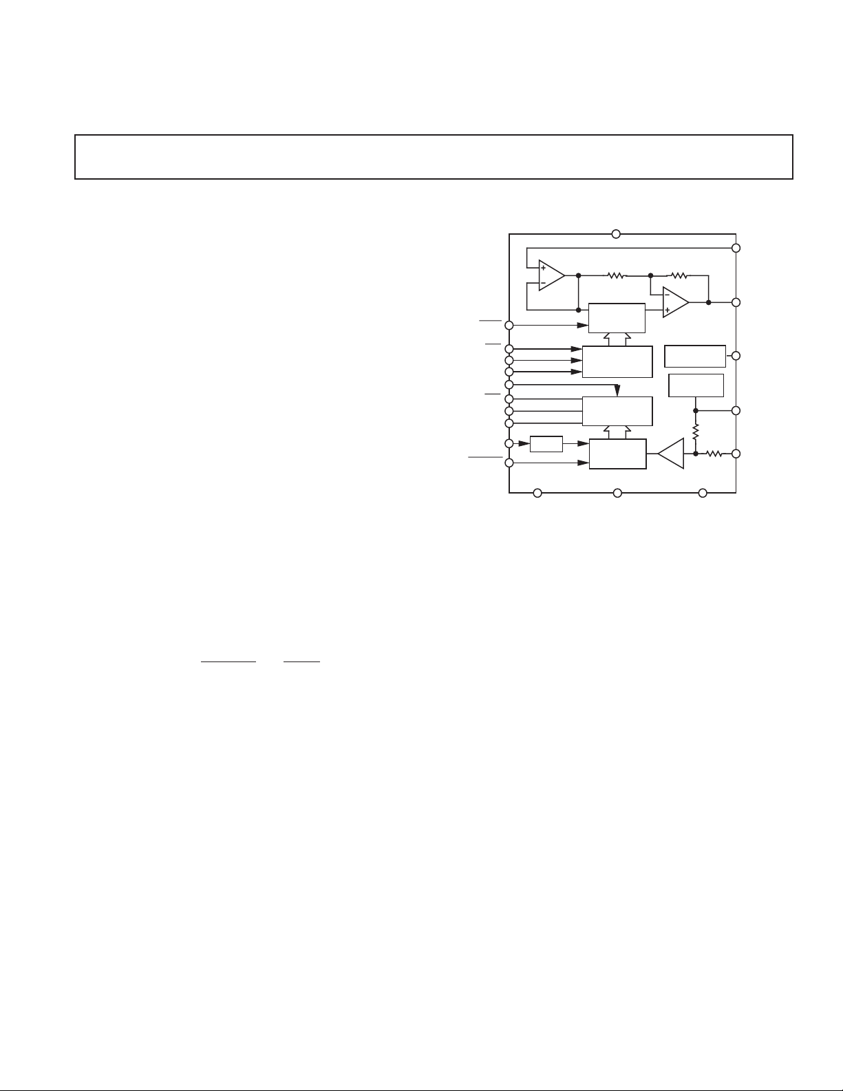
Complete, 14-Bit Analog I/O System
FEATURES
Complete 14-Bit l/O System, Comprising
14-Bit ADC with Track/Hold Amplifier
83 kHz Throughput Rate
14-Bit DAC with Output Amplifier
3.5 ms Settling Time
On-Chip Voltage Reference
Operates from 65 V Supplies
Low Power—130 mW typ
Small 0.3" Wide DIP
APPLICATIONS
Digital Signal Processing
Speech Recognition and Synthesis
Spectrum Analysis
High Speed Modems
DSP Servo Control
GENERAL DESCRIPTION
The AD7869 is a complete 14-bit I/O system containing a DAC
and an ADC. The ADC is a successive approximation type with
a track-and-hold amplifier, having a combined throughput rate
of 83 kHz. The DAC has an output buffer amplifier with a settling time of 4 µs to 14 bits. Temperature compensated 3 V bur-
ied Zener references provide precision references for the DAC
and ADC.
Interfacing to both the DAC and ADC is serial, minimizing pin
count and giving a small 24-pin package size. Standard control
signals allow serial interfacing to most DSP machines.
Asynchronous ADC conversion control and DAC updating is
made possible with the
CONVST and LDAC logic inputs.
The AD7869 operates from ±5 V power supplies; the analog input/output range of the ADC/DAC is ±3 V. The part is fully
specified for dynamic parameters such as signal-to-noise ratio
and harmonic distortion as well as traditional dc specifications.
The part is available in a 24-pin, 0.3 inch wide, plastic or hermetic dual-in-line package (DIP) and in a 28-pin, plastic SOIC
package.
AD7869
FUNCTIONAL BLOCK DIAGRAM
PRODUCT HIGHLIGHTS
1. Complete 14-Bit I/O System.
The AD7869 contains a 14-bit ADC with a track-and-hold
amplifier and a 14-bit DAC with output amplifier. Also in
cluded are separate on-chip voltage references for the DAC
and the ADC.
2. Dynamic Specifications for DSP Users.
In addition to traditional dc specifications, the AD7869 is
specified for ac parameters, including signal-to-noise ratio
and harmonic distortion. These parameters, along with important timing parameters, are tested on every device.
3. Small Package.
The AD7869 is available in a 24-pin DIP and a 28-pin SOIC
package.
REV. A
Information furnished by Analog Devices is believed to be accurate and
reliable. However, no responsibility is assumed by Analog Devices for its
use, nor for any infringements of patents or other rights of third parties
which may result from its use. No license is granted by implication or
otherwise under any patent or patent rights of Analog Devices.
One Technology Way, P.O. Box 9106, Norwood, MA 02062-9106, U.S.A.
Tel: 617/329-4700 World Wide Web Site: http://www.analog.com
Fax: 617/326-8703 © Analog Devices, Inc., 1996
Page 2
AD7869–SPECIFICA TIONS
(VDD = +5 V 6 5%, VSS = –5 V 6 5%, AGND = DGND = 0 V, f
ADC SECTION
Parameter J Version1A Version1Units Test Conditions/Comments
DYNAMIC PERFORMANCE
Signal-to-Noise Ratio
T
to T
MIN
Total Harmonic Distortion (THD) –86 –86 dB typ V
Peak Harmonic or Spurious Noise –86 –86 dB typ V
Intermodulation Distortion (IMD)
Second Order Terms –86 –86 dB typ fa = 9 kHz, fb = 9.5 kHz, f
Third Order Terms –88 –88 dB typ fa = 9 kHz, fb = 9.5 kHz, f
Track/Hold Acquisition Time 2 2 µs max
DC ACCURACY
Resolution 14 14 Bits
Minimum Resolution 14 14 Bits No Missing Codes Are Guaranteed
Integral Nonlinearity ±2 ±2 LSB max
Differential Nonlinearity ±1 ±1 LSB max
Bipolar Zero Error ±20 ±20 LSB max
Positive Gain Error
Negative Gain Error
ANALOG INPUT
Input Voltage Range ±3 ±3 Volts
Input Current ±1 ±1 mA max
REFERENCE OUTPUT
RO ADC @ +25°C 2.99/3.01 2.99/3.01 V min/ V max
RO ADC TC ±25 ±25 ppm/°C typ
Reference Load Sensitivity
(∆RO ADC vs. ∆I) –1.5 –1.5 mV max Reference Load Current Change (0–500 µA),
LOGIC INPUTS
(
CONVST, CLK, CONTROL)
Input High Voltage, V
Input Low Voltage, V
Input Current, I
Input Current7 (CONTROL & CLK) ±10 ±10 µA max VIN = VSS to DGND
Input Capacitance, C
LOGIC OUTPUTS
DR,
Output Low Voltage, V
RCLK Output
Output Low Voltage, V
DR,
Floating-State Leakage Current ±10 ±10 µA max
Floating-State Output Capacitance
CONVERSION TIME
External Clock 10 10 µs max
Internal Clock 10 10 µs max The Internal Clock Has a Nominal Value of 2.0 MHz
POWER REQUIREMENTS For Both DAC and ADC
V
DD
V
SS
I
DD
I
SS
Total Power Dissipation 170 170 mW max Typically 130 mW
NOTES
1
Temperature ranges are as follows: J Version, 0°C to +70° C; A Version, –40°C to +85 °C.
2
VIN = ±3 V.
3
SNR calculation includes distortion and noise components.
4
SNR degradation due to asynchronous DAC updating during conversion is 0.1 dB typ.
5
Measured with respect to internal reference.
6
For capacitive loads greater than 50 pF, a series resistor is required (see Internal Reference section).
7
Tying the CONTROL input to VDD places the device in a factory test mode where normal operation is not exhibited.
8
Sample tested @ +25°C to ensure compliance.
Specifications subject to change without notice.
MAX
RFS Outputs
RFS, RCLK Outputs
All specifications T
2
3, 4
(SNR) @ +25°C 78 78 dB min VIN = 10 kHz Sine Wave, f
MIN
to T
unless otherwise noted.)
MAX
78 77 dB min
5
5
6
±20 ±20 LSB max
±20 ±20 LSB max
±40 ±ppm/°C max
INH
INL
IN
8
IN
OL
OL
2.4 2.4 V min VDD = 5 V ± 5%
0.8 0.8 V max VDD = 5 V ± 5%
±10 ±10 µA max VIN = 0 V to V
10 10 pF max
0.4 0.4 V max I
0.4 0.4 V max I
8
15 15 pF max
+5 +5 V nom ±5% for Specified Performance
–5 –5 V nom ±5% for Specified Performance
22 22 mA max Cumulative Current from the Two VDD Pins
12 12 mA max Cumulative Current from the Two VSS Pins
= 2.0 MHz external.
CLK
= 10 kHz Sine Wave, f
IN
= 10 kHz Sine Wave, f
IN
Reference Load Should Not Be Changed
During Conversion
DD
= 1.6 mA, Pull-Up Resistor = 4.7 kΩ
SINK
= 2.6 mA, Pull-Up Resistor = 2 kΩ
SINK
SAMPLE
SAMPLE
SAMPLE
SAMPLE
SAMPLE
= 83 kHz
= 83 kHz
= 83 kHz
= 50 kHz
= 50 kHz
–2–
REV. A
Page 3
AD7869
(VDD = +5 V 6 5%, VSS = –5 V 6 5%, AGND = DGND = 0 V, Rl DAC = +3 V and decoupled as shown in Figure 2,
V
DAC SECTION
Load to AGND; = 2 kV, CL = 100 pF. All specifications T
OUT
Parameter J Versions1A Version1Units Test Conditions/Comments
DYNAMIC PERFORMANCE
2
Signal-to-Noise Ratio3 (SNR) @ +25°C 78 78 dB min V
to T
T
MIN
MAX
78 77 dB min Typically 82 dB at +25°C for 0 < V
Total Harmonic Distortion (THD) –86 –86 dB typ V
Peak Harmonic or Spurious Noise –86 –86 dB typ V
DC ACCURACY
Resolution 14 14 Bits
Integral Nonlinearity ±2 ± 2 LSB max
Differential Nonlinearity ±1 ± 1 LSB max Guaranteed Monotonic
Bipolar Zero Error ±10 ±10 LSB max
Positive Full-Scale Error
Negative Full-Scale Error
REFERENCE OUTPUT
5
5
6
±10 ±10 LSB max
±10 ±10 LSB max
RO DAC @ +25°C 2.99/3.01 2.99/3.01 V min/V max
RO DAC TC ±25 ±25 ppm/°C typ
±40 ppm/°C max
Reference Load Change
(∆RO DAC vs. ∆I) –1.5 –1.5 mV max Reference Load Current Change (0 µA–500 µA)
REFERENCE INPUT
RI DAC Input Range 2.85/3.15 2.85/3.15 V min/V max 3 V ± 5%
Input Current 1 1 µA max
LOGIC INPUTS
LDAC, TFS, TCLK, DT)
(
Input High Voltage, V
Input Low Voltage, V
Input Current, I
Input Capacitance, C
INL
IN
IN
INH
7
2.4 2.4 V min VDD = 5 V ± 5%
0.8 0.8 V max VDD = 5 V ± 5%
±10 ±10 µA max VIN = 0 V to V
10 10 pF max
ANALOG OUTPUT
Output Voltage Range ±3 ±3 V nom
DC Output Impedance 0.3 0.3 Ω typ
Short-Circuit Current 20 20 mA typ
AC CHARACTERISTICS
7
Voltage Output Settling-Time Settling Time to Within ±1/2 LSB of Final Value
Positive Full-Scale Change 4 4 µs max Typically 3 µs
Negative Full-Scale Change 4 4 µs max Typically 3.5 µs
Digital-to-Analog Glitch Impulse 10 10 nV secs typ DAC Code Change All 1s to All 0s
Digital Feedthrough 2 2 nV secs typ
VIN to V
Isolation 100 100 dB typ VIN = ±3 V, 41.5 kHz Sine Wave
OUT
POWER REQUIREMENTS As per ADC Section
NOTES
1
Temperature ranges are as follows: J Version, 0°C to +70° C; A Version, –40°C to +85 °C.
2
V
(p-p) = ±3 V.
OUT
3
SNR calculation includes distortion and noise components.
4
Using external sample and hold, see Figures 13 to 15.
5
Measured with respect to REF IN and includes bipolar offset error.
6
For capacitive loads greater than 50 pF a series resistor is required (see Internal Reference section).
7
Sample tested @ +25°C to ensure compliance.
Specifications subject to change without notice
to T
MIN
unless otherwise noted.)
MAX
= 1 kHz Sine Wave, f
OUT
= 1 kHz Sine Wave, f
OUT
Typically –84 dB at +25°C for 0 < V
= 1 kHz, f
OUT
SAMPLE
Typically –84 dB at +25°C for 0 < V
DD
SAMPLE
SAMPLE
= 83 kHz
= 83 kHz
< 20 kHz
OUT
= 83 kHz
< 20 kHz
OUT
< 20 kHz
OUT
4
4
4
REV. A
–3–
Page 4
AD7869
MIN
1, 2
(VDD = +5 V 6 5%, VSS = –5 V 6 5%, AGND = DGND = 0 V)
, T
MAX
TIMING SPECIFICATIONS
Limit at T
Parameter (All Versions) Units Conditions/Comments
ADC TIMING
t
1
3
t
2
t
3
t
4
4
t
5
t
6
5
t
13
DAC TIMING
t
7
t
8
t
9
t
10
t
11
t
l2
NOTES
1
Timing specifications are sample tested at +25°C to ensure compliance. All input signals are specified with tr = tf = 5 ns (10% to 90% of 5 V) and timed from a
voltage level of 1.6 V.
2
Serial timing is measured with a 4.7 kΩ pull-up resistor on DR and RFS and a 2 k Ω pull-up resistor on RCLK. The capacitance on all three outputs is 35 pF.
3
When using internal clock, RCLK mark/space ratio (measured form a voltage level of 1.6 V) range is 40/60 to 60/40. For external clock, RCLK mark/space
ratio = external clock mark/space ratio.
4
DR will drive higher capacitance loads but this will add to t5 since it increases the external RC time constant (4.7 k Ω//CL) and hence the time to reach 2.4 V.
5
Time 2 RCLK to 3 RCLK depends on conversion start to ADC clock synchronization.
6
TCLK mark/space ratio is 40/60 to 60/40.
50 ns min CONVST Pulse Width
440 ns min RCLK Cycle Time, Internal Clock
100 ns min RFS to RCLK Falling Edge Setup Time
20 ns min RCLK Rising Edge to RFS
100 ns max
155 ns max RCLK to Valid Data Delay, CL = 35 pF
4 ns min Bus Relinquish Time after RCLK
100 ns max
2 RCLK + 200 to ns typ CONVST to RFS Delay
3 RCLK + 200
50 ns min TFS to TCLK Falling Edge
75 ns min TCLK Falling Edge to TFS
150 ns min TCLK Cycle Time
30 ns min Data Valid to TCLK Setup Time
75 ns min Data Valid to TCLK Hold Time
40 ns min LDAC Pulse Width
ABSOLUTE MAXIMUM RATINGS*
(TA = + 25°C unless otherwise noted)
VDD to AGND . . . . . . . . . . . . . . . . . . . . . . . . . –0.3 V to +7 V
V
to AGND . . . . . . . . . . . . . . . . . . . . . . . . . +0.3 V to –7 V
SS
AGND to DGND . . . . . . . . . . . . . . . . –0.3 V to V
V
to AGND . . . . . . . . . . . . . . . . . . . . . . . . . . . VSS to V
OUT
VIN to AGND . . . . . . . . . . . . . . . . V
–0.3 V to VDD + 0.3 V
SS
RO ADC to AGND . . . . . . . . . . . . . . . –0.3 V to V
RO DAC to AGND . . . . . . . . . . . . . . . –0.3 V to V
RI DAC to AGND . . . . . . . . . . . . . . . –0.3 V to V
Digital Inputs to DGND . . . . . . . . . . . –0.3 V to V
Digital Outputs to DGND . . . . . . . . . . –0.3 V to V
+ 0.3 V
DD
+ 0.3 V
DD
+ 0.3 V
DD
+ 0.3 V
DD
+ 0.3 V
DD
+ 0.3 V
DD
DD
Operating Temperature Range
J Version . . . . . . . . . . . . . . . . . . . . . . . . . . . . 0°C to +70°C
A Version . . . . . . . . . . . . . . . . . . . . . . . . . . –40°C to +85°C
Storage Temperature Range . . . . . . . . . . . . –65°C to +150°C
Lead Temperature (Soldering, 10 secs) . . . . . . . . . . . +300°C
Power Dissipation (Any Package) to +75°C . . . . . . . 1000 mW
Derates above +75°C by . . . . . . . . . . . . . . . . . . . . 10 mW/°C
*Stresses above those listed under “Absolute Maximum Ratings” may cause
permanent damage to the device. This is a stress rating only; functional operation
of the device at these or any other conditions above those listed in the operational
sections of this specification is not implied. Exposure to absolute maximum rating
conditions for extended periods may affect device reliability.
CAUTION
ESD (electrostatic discharge) sensitive device. Electrostatic charges as high as 4000 V readily
accumulate on the human body and test equipment and can discharge without detection.
Although the AD7869 features proprietary ESD protection circuitry, permanent damage may
occur on devices subjected to high energy electrostatic discharges. Therefore, proper ESD
precautions are recommended to avoid performance degradation or loss of functionality.
ORDERING GUIDE
Signal-
Temperature to-Noise Relative Package
Model Range Ratio (SNR) Accuracy Option*
AD7869JN 0°C to +70°C 78 dB ±2 LSB max N-24
AD7869JR 0°C to +70°C 78 dB ±2 LSB max R-28
AD7869AQ –40°C to +85°C 77 dB ±2 LSB max Q-24
*N = Plastic DIP; Q = Cerdip; R = Small Outline IC (SOIC).
WARNING!
ESD SENSITIVE DEVICE
–4–
REV. A
Page 5
AD7869
0.01 (0.254)
0.006 (0.15)
0.019 (0.49)
0.014 (0.35)
0.096 (2.44)
0.089 (2.26)
0.05
(1.27)
BSC
0.013 (0.32)
0.009 (0.23)
0.042 (1.067)
0.018 (0.457)
6°
0°
0.03 (0.76)
0.02 (0.51)
x 45°
0.708 (18.02)
0.696 (17.67)
0.414 (10.52)
0.398 (10.10)
0.299 (7.6)
0.291 (7.39)
28 15
141
1. LEAD NO. 1 INDENTIFIED BY A DOT.
2. SOIC LEADS WILL BE EITHER TIN PLATED OR SOLDER DIPPED
IN ACCORDANCE WITH MIL-M-38510 REQUIREMENTS.
AD7869 PIN FUNCTION DESCRIPTION
DIP Pin
Number Mnemonic Function
POWER SUPPLY
7 & 23 V
10 & 22 V
DD
SS
8 & 19 AGND Analog Ground. Both AGND pins must be tied together.
6 & 17 DGND Digital Ground. Both DGND pins must be tied together.
ANALOG SIGNAL AND REFERENCE
21 V
9V
IN
OUT
20 RO ADC Voltage Reference Output. The internal ADC 3 V reference is provided at this pin. This output may be used as a
11 RO DAC DAC Voltage Reference Output. This is one of two internal voltage references. To operate the DAC with this
12 RI DAC DAC Voltage Reference Input. The voltage reference for the DAC must be applied to this pin. It is internally
ADC INTERFACE AND CONTROL
2 CLK Clock Input. An external TTL-compatible clock may be applied to this input. Alternatively, tying this pin to V
3
RFS Receive Frame Synchronization, Logic Output. This is an active low open-drain output that provides a framing
4 RCLK Receive Clock, Logic Output. RCLK is the gated serial clock output that is derived from the internal or external
5 DR Receive Data, Logic Output. This is an open-drain data output used in conjunction with
1
CONVST Convert Start, Logic Input. A low to high transition on this input puts the track-and-hold amplifier into the hold
24 CONTROL Control, Logic Input. With this pin at 0 V, the RCLK is noncontinuous. With this pin at –5 V, the RCLK is contin-
DAC INTERFACE AND CONTROL
14
TFS Transmit Frame Synchronization, Logic Input. This is a frame or synchronization signal for the DAC with serial
15 DT Transmit Data, Logic Input. This is the data input that is used in conjunction with
16 TCLK Transmit Clock, Logic Input. Serial data bits are latched on the falling edge of TCLK when
13
LDAC Load DAC, Logic Input. A new word is transferred into the DAC latch from the input latch on the falling edge
18 NC No Connect.
Positive Power Supply, 5 V ± 5%. Both VDD pins must be tied together.
Negative Power Supply, –5 V ± 5%. Both VSS pins must be tied together.
ADC Analog Input. The ADC input range is ±3 V.
Analog Output Voltage from DAC. This output comes from a buffer amplifier. The range is bipolar, ±3 V
with RI DAC = +3 V.
reference for the DAC by connecting it to the RI DAC input. The external load capability of this reference is 500 µA.
internal reference, RO DAC should be connected to RI DAC. The external load capability of the reference is 500 µA.
buffered before being applied to the DAC. The nominal reference voltage for correct operation of the AD7869 is 3 V.
enables the internal laser-trimmed oscillator.
SS
pulse for serial data. An external 4.7 kΩ pull-up resistor is required on
ADC clock. If the CONTROL input is at V
, the clock runs continuously. With the CONTROL input at DGND,
SS
RFS.
the RCLK output is gated off (three-state) after serial transmission is complete. RCLK is an open-drain output and
requires an external 2 kΩ pull-up resistor.
RFS and RCLK to transmit
data from the ADC. Serial data is valid on the falling edge of RCLK when
RFS is low. An external 4.7 kΩ resistor is
required on the DR output.
mode and starts an ADC conversion. This input is asynchronous to the CLK input.
uous. Note, tying this pin to VDD places the part in a factory test mode where normal operation is not exhibited.
data expected after the falling edge of this signal.
TFS and TCLK to transfer
serial data to the input latch.
TFS is low.
of this signal.
CONVST
REV. A
RCLK
DGND
AGND
RO DAC
RI DAC
V
CLK
RFS
V
V
DR
OUT
1
2
3
4
5
6
7
DD
8
9
10
SS
11
12
DIP
AD7869
TOP VIEW
(Not to Scale)
NC = NO CONNECT
24
23
22
21
20
19
18
17
16
15
14
13
CONTROL
V
DD
V
SS
V
IN
RO ADC
AGND
NC
DGND
TCLK
DT
TFS
LDAC
PIN CONFIGURATIONS
SOIC
–5–
Page 6

AD7869
CONVERTER DETAILS
The AD7869 is a complete 14-bit I/O port; the only external
components required for normal operation are pull-up resistors
for the ADC data outputs, and power supply decoupling capacitors. The AD7869 is comprised of a 14-bit successive approximation ADC with a track/hold amplifier, a 14-bit DAC with a
buffered output and two 3 V buried Zener references, a clock oscillator and control logic.
ADC CLOCK
The AD7869 has an internal clock oscillator that can be used for
the ADC conversion procedure. The oscillator is enabled by tying the CLK input to V
. The oscillator is laser trimmed at the
SS
factory to give a maximum conversion time of 10 µs. The mark/
space ratio can vary from 40/60 to 60/40. Alternatively, an external TTL compatible clock may be applied to this input. The allowable mark/space ratio of an external clock is 40/60 to 60/40.
RCLK is a clock output, used for the serial interface. This output is derived directly from the ADC clock source and can be
switched off at the end of conversion with the CONTROL
input.
ADC CONVERSION TIMING
The conversion time for both external clock and continuous internal clock can vary from 19 to 20 rising clock edges, depending
on the conversion start to ADC clock synchronization. If a conversion is initiated within 30 ns prior to a rising edge of the ADC
clock, the conversion time will consist of 20 rising clock edges,
i.e., 9.5 µs conversion time. For noncontinuous internal clock,
the conversion time always consists of 19 rising clock edges.
The operation of the track/hold amplifier is essentially transparent to the user. The track/hold amplifier goes from its track
mode to its hold mode at the start of conversion on the rising
edge of
CONVST.
INTERNAL REFERENCES
The AD7869 has two on-chip temperature compensated buried
Zener references that are factory trimmed to 3 V ±10 mV. One
reference provides the appropriate biasing for the ADC, while
the other is available as a reference for the DAC. Both reference
outputs are available (labelled RO DAC and RO ADC) and are
capable of providing up to 500 µA to an external load.
The DAC input reference (RI DAC) can be sourced externally
or connected to any of the two on-chip references. Applications
requiring good full-scale error matching between the DAC and
the ADC should use the ADC reference as shown in Figure 4.
The maximum recommended capacitance on either of the reference output pins for normal operation is 50 pF. If either of the
reference outputs is required to drive a capacitive load greater
than 50 pF, then a 200 Ω resistor must be placed in series with
the capacitive load. The addition of decoupling capacitors,
10 µF in parallel with 0.1 µF as shown in Figure 2, improves
noise performance. The improvement in noise performance can
be seen from the graph in Figure 3. Note: this applies for the
DAC output only; reference decoupling components do not affect ADC performance. Consequently, a typical application will
have just the DAC reference decoupled with the other one open
circuited.
ADC TRACK-AND-HOLD AMPLIFIER
The track-and-hold amplifier on the analog input of the AD7869
allows the ADC to accurately convert an input sine wave of 6 V
peak–peak amplitude to 14-bit accuracy. The input impedance is
typically 9 kΩ; an equivalent circuit is shown in Figure 1. The
input bandwidth of the track/hold amplifier is much greater
than the Nyquist rate of the ADC even when the ADC is operated at its maximum throughput rate. The 0.1 dB cutoff frequency occurs typically at 500 kHz. The track/hold amplifier
acquires an input signal to 14-bit accuracy in less than 2 µs. The
overall throughput rate is equal to the conversion time plus the
track/hold amplifier acquisition time. For a 2.0 MHz input clock,
the throughput time is 12 µs max.
TRACK/HOLD
V
IN
4.5kΩ
4.5kΩ
*ADDITIONAL PINS OMITTED FOR CLARITY
AMPLIFIER
TO INTERNAL
3V REFERENCE
TO INTERNAL
COMPARATOR
AD7869*
Figure 1. ADC Analog Input
RI DAC
RO DAC
or
RO ADC*
*RO DAC/RO ADC CAN BE LEFT
OPEN CIRCUIT IF NOT USED
200Ω
10µF
EXT LOAD
GREATER THAN 50pF
0.1µF
Figure 2. Reference Decoupling Components
DAC OUTPUT AMPLIFIER
The output from the voltage mode DAC is buffered by a noninverting amplifier. The buffer amplifier is capable of developing
±3 V across 2 kΩ and 100 pF load to ground and can produce
6 V peak-to-peak sine wave signals to a frequency of 20 kHz.
The output is updated on the falling edge of the LDAC input.
The output voltage settling time, to within 1/2 LSB of its final
value, is typically less than 3.5 µs.
The small signal (200 mV p–p) bandwidth of the output buffer
amplifier is typically 1 MHz. The output noise from the amplifier is low with a figure of 30 nV/√
Hz at a frequency of 1 kHz.
The broadband noise from the amplifier exhibits a typical peakto-peak figure of 150 µV for a 1 MHz output bandwidth. Figure
3 shows a typical plot of noise spectral density versus frequency
for the output buffer amplifier and for either of the on-chip
references.
–6–
REV. A
Page 7

AD7869
500
TA = +25°C
= +5V
V
DD
V
200
100
nV – √Hz
50
20
10
50 100 200
REF OUT
OUTPUT WITH
ALL 0s LOADED
REF OUT DECOUPLED
AS SHOWN IN
FIGURE 2
1k 2k
FREQUENCY – Hz
= –5V
SS
10k
20k
100k
Figure 3. Noise Spectral Density vs. Frequency
INPUT/OUTPUT TRANSFER FUNCTIONS
A bipolar circuit for the AD7869 is shown in Figure 4.
The analog input/output voltage range of the AD7869 is ±3 V.
The designed code transitions for the ADC occur midway between successive integer LSB values (i.e., 1/2 LSB, 3/2 LSB,
5/2 LSB . . . FS –3/2 LSBs). The input/output code is 2s
Complement Binary with 1 LSB = FS/16384 = 366 µV. The
ideal transfer function is shown in Figure 5.
ANALOG INPUT
RANGE = ±3V
V
IN
RI DAC
R1
200
RO ADC
C2
C1
10µF
0.1µF
AGND
*ADDITIONAL PINS OMITTED FOR CLARITY
AD7869*
V
OUT
ANALOG OUTPUT
RANGE = ±3V
Figure 4. Basic Bipolar Operation
OUTPUT
CODE
011...111
011...110
000...010
-FS
000...001
000...000
111...111
111...110
100...001
100...000
2
0V
INPUT VOLTAGE
1LSB =
+
FS
2
FS = 6V
-1LSB
16384
FS
Figure 5. Input/Output Transfer Function
OFFSET AND FULL SCALE ADJUSTMENT
In most digital signal processing (DSP) applications, offset and
full-scale errors have little or no effect on system performance.
Offset error can always be eliminated in the analog domain by
ac coupling. Full-scale errors do not cause problems as long as
the input signal is within the full dynamic range of the ADC.
For applications requiring that the input signal range match the
full analog input dynamic range of the ADC, offset and fullscale errors have to be adjusted to zero.
ADC ADJUSTMENT
Figure 6 has signal conditioning at the input and output of the
AD7869 for trimming the endpoints of the transfer functions of
both the ADC and the DAC. Offset error must be adjusted before full-scale error. For the ADC, this is achieved by trimming
the offset of A1 while the input voltage, V1, is 1/2 LSB below
ground. The trim procedure is as follows: apply a voltage of
–183 µV (–1/2 LSB) at V1 in Figure 6 and adjust the offset volt-
age of A1 until the ADC output code flickers between 11 1111
1111 1111 (3FFF HEX) and 00 0000 0000 0000 (0000 HEX).
V1
INPUT VOLTAGE
RANGE = ±3V
R1
10k
R2
500
R3
10k
R5
10k
*ADDITIONAL PINS
OMITTED FOR
CLARITY
A1
R4
10k
V
IN VOUT
AD7869*
AGND
10k
500
10k
R6
R7
R8
R10
10k
A2
R9
10k
V0
OUTPUT VOLTAGE
RANGE = ± 3V
Figure 6. AD7869 with Input/Output Adjustment
ADC gain error can be adjusted at either the first code transition (ADC negative full scale) or the last code transition (ADC
positive full scale). The trim procedures for both cases are as
follows (see Figure 6).
ADC Positive Full-Scale Adjustment
Apply a voltage of 2.99945 V (FS/2 – 3/2 LSBs) at V1. Adjust
R2 until the ADC output code flickers between 01 1111 1111
1110 (1FFE HEX) and 01 1111 1111 1111 (1FFF HEX).
ADC Negative Full-Scale Adjustment
Apply a voltage of –2.99982 V (–FS/2 + 1/2 LSB) at V1 and adjust R2 until the ADC output code flickers between 10 0000
0000 0000 (2000 HEX) and 10 0000 0000 0001 (2001 HEX).
DAC ADJUSTMENT
Op amp A2 is included in Figure 6 for the DAC transfer function adjustment. Again, offset must be adjusted before full scale.
To adjust offset, load the DAC with 00 0000 0000 0000 (0000
HEX) and trim the offset of A2 to 0 V. As with the ADC adjustment, gain error can be adjusted at either the first code transition (DAC negative full scale) or the last code transition (DAC
positive full scale). The trim procedures for both cases are as
follows:
DAC Positive Full-Scale Adjustment
Load the DAC with 01 1111 1111 1111 (1FFF HEX) and adjust R7 until the op amp output voltage is equal to 2.99963 V
(FS/2 – 1 LSB).
DAC Negative Full-Scale Adjustment
Load the DAC with 10 0000 0000 0000 (2000 HEX) and adjust
R7 until the op amp output voltage is equal to –3 V (–FS/2).
REV. A
–7–
Page 8

AD7869
TIMING AND CONTROL
Communication with the AD7869 is managed by six dedicated
pins. These consist of separate serial clocks, word framing or
strobe pulses, and data signals for both receiving and transmitting data. Conversion starts and DAC updating are controlled
by two digital inputs,
CONVST and LDAC. These inputs can
be asserted independently of the microprocessor by an external
timer when precise sampling intervals are required. Alternatively, the
LDAC and CONVST can be driven from a decoded
address bus, allowing the microprocessor control over conversion start and DAC updating as well as data communication to
the AD7869.
ADC Timing
Conversion control is provided by the CONVST input. A low to
high transition on
CONVST input starts conversion and drives
the track/hold amplifier into its hold mode. Serial data then becomes available while conversion is in progress. The corresponding timing diagram is shown in Figure 7. The word length
is 16 bits, two leading zeros followed by the 14-bit conversion
result starting with the MSB. The data is synchronized to the
serial clock output (RCLK) and is framed by the serial strobe
(
RFS). Data is clocked out on a low to high transition of the serial clock and is valid on the falling edge of this clock while the
RFS output is low. RFS goes low at the start of conversion, and
the first serial data bit (which is the first leading zero) is valid on
the first falling edge of RCLK. All the ADC serial lines are
open-drain outputs and require external pull-up resistors.
CONVERSION TIME
t
13
t
3
t
5
DB13 DB12 DB11 DB1 DB0
t
2
t
4
t
6
CONVST
RFS
RCLK
DR
t
1
1
2,3
1
Figure 7. ADC Control Timing Diagram
The serial clock out is derived from the ADC master clock
source, which may be internal or external. Normally, RCLK is
required during the serial transmission only. In these cases, it
can be shut down (i.e., placed into three-state) at the end of
conversion to allow multiple ADCs to share a common serial
bus. However, some serial systems (e.g., TMS32020) require a
serial clock that runs continuously. Both options are available
on the AD7869 ADC. With the CONTROL input at 0 V,
RCLK is noncontinuous; when it is at –5 V, RCLK is
continuous.
DAC TIMING
The AD7869 DAC contains two latches, an input latch and a
DAC latch. Data must be loaded to the input latch under the
control of the TCLK,
TFS and DT serial logic inputs. Data is
then transferred from the input latch to the DAC latch under
the control of the
LDAC signal. Only the data in the DAC latch
determines the analog output of the AD7869.
Data is loaded to the input latch under control of TCLK,
TFS
and DT. The AD7869 DAC expects a 16-bit stream of serial
data on its DT input. Data must be valid on the falling edge of
TCLK. The
TFS input provides the frame synchronization signal, which tells the AD7869 DAC that valid serial data will be
available for the next 16 falling edges of TCLK. Figure 8 shows
the timing diagram for the serial data format.
TFS
TCLK
DT
t
7
DON'T
CARE
t
DON'T
CARE
9
DB13 DB12
t
11
t
10
DB11 DB10 DB1 DB0
t
8
Figure 8. DAC Control Timing Diagram
Although 16 bits of data are clocked into the input latch, only
14 bits are transferred into the DAC latch. Therefore, two bits
in the stream are don’t cares since their value does not affect the
DAC latch data. The bit positions are two don’t cares, followed
by the 14-bit DAC data starting with the MSB.
The
LDAC signal controls the transfer of data to the DAC
latch. Normally, data is loaded to the DAC latch on the falling
edge of
LDAC. However, if LDAC is held low, then serial data
is loaded to the DAC latch on the sixteenth falling edge of
TCLK. If
LDAC goes low during the loading of serial data to
the input latch, no DAC latch update takes place on the falling
edge of
LDAC. If LDAC stays low until the serial transfer is
completed, the update takes place on the sixteenth falling edge
of TCLK. If
LDAC returns high before the serial data transfer
is completed, no DAC latch update takes place.
–8–
REV. A
Page 9

AD7869
DAC
LOW-PASS
FILTER
16-BIT
DIGITIZER
MICRO-
CONTROLLER
AD7869 DYNAMIC SPECIFICATIONS
The AD7869 is specified and 100% tested for dynamic performance specifications as well as traditional dc specifications such
as Integral and Differential Nonlinearity. These ac specifications
are required for signal processing applications such as speech
recognition, spectrum analysis and high speed modems. These
applications require information on the converter’s effect on the
spectral content of the input signal. Hence, the parameters for
which the AD7869 is specified include SNR, harmonic distortion and peak harmonics. These terms are discussed in more detail in the following sections.
Signal-to-Noise Ratio (SNR)
SNR is the measured signal-to-noise ratio at the output of the
ADC or DAC. The signal is the rms magnitude of the fundamental. Noise is the rms sum of all the nonfundamental signals
up to half the sampling frequency (f
/2), excluding dc.
SAMPLE
SNR is dependent upon the number of levels used in the quantization process; the more levels, the smaller the quantization
noise. The theoretical signal-to-noise ratio for a sine wave input
is given by
SNR = (6.02N + 1.76) dB (1)
where N is the number of bits. Thus for an ideal 14-bit converter, SNR = 86 dB.
Effective Number of Bits
The formula given in Equation (1) relates the SNR to the number of bits. Rewriting the formula, as in Equation (2), it is possible to obtain a measure of performance expressed in effective
number of bits (N).
SNR–1.76
N =
6.02
(2)
The effective number of bits for a device can be calculated directly from its measured SNR.
Harmonic Distortion
Harmonic Distortion is the ratio of the rms sum of harmonics to
the fundamental. For the AD7869, total harmonic distortion
(THD) is defined as:
2
2
THD =20 log
2
2
+V
+V
V
2
3
+V
4
V
1
2
+V
5
6
where V1 is the rms amplitude of the fundamental and V2, V3,
V4, V5 and V6 are the rms amplitudes of the second through to
the sixth harmonic. The THD is also derived from the FFT plot
of the ADC or DAC output spectrum.
ADC Testing
The output spectrum from the ADC is evaluated by applying a
sine wave signal of very low distortion to the V
input while
IN
reading multiple conversion results. A Fast Fourier Transform
(FFT) plot is generated from which the SNR data can be obtained. Figure 9 shows a typical 2048 point FFT plot of the
AD7869AQ ADC with an input signal of 10 kHz and a sampling frequency of 60 kHz. The SNR obtained from this graph
is 80 dB. It should be noted that the harmonics are taken into
account when calculating the SNR.
AD7869
Figure 9. ADC FFT Plot
Figure 10 shows a typical plot of effective number of bits versus
frequency for an AD7869AQ with a sampling frequency of
60 kHz. The effective number of bits typically falls between 12.7
and 13.1, corresponding to SNR figures of 79 dB and 80.4 dB.
Figure 10. Effective Number of Bits vs. Frequency for the
ADC
DAC Testing
A simplified diagram of the method used to test the dynamic
performance specifications of the DAC is outlined in Figure 11.
Data is loaded to the DAC under control of the microcontroller
and associated logic. The output of the DAC is applied to a 9th
order low pass filter whose cutoff frequency corresponds to the
Nyquist limit. The output of the filter is, in turn, applied to a
16-bit accurate digitizer. This digitizes the signal and the microcontroller generates an FFT plot from which the dynamic performance of the DAC can be evaluated.
Figure 11. DAC Dynamic Performance Test Circuit
REV. A
–9–
Page 10

AD7869
The digitizer sampling is synchronized with the DAC update
rate to ease FFT calculations. The digitizer samples the DAC
output after the output has settled to its new value. Therefore, if
the digitizer were to directly sample the output, it would effectively be sampling a dc value each time. As a result, the dynamic
performance of the DAC would not be measured correctly. Using the digitizer directly on the DAC output would give better
results than the actual performance of the DAC. Using a filter
between the DAC and the digitizer means that the digitizer
samples a continuously moving signal, and the true dynamic
performance of the AD7869 DAC output is measured.
Figure 12 shows a typical 2048 point Fast Fourier Transform
plot for the AD7869 DAC with an update rate of 83 kHz and an
output frequency of 1 kHz. The SNR obtained from the graph is
82 dBs.
Performance versus Frequency
The typical performance plots of Figures 14 and 15 show the
AD7869 DAC performance over a wide range of input frequencies at an update rate of 83 kHz. The plot of Figure 14 is without a sample-and-hold on the DAC output while the plot of
Figure 15 is generated with a sample-and-hold on the output.
Figure 14. DAC Performance vs. Frequency (No
Sample-and-Hold)
Figure 12. DAC FFT Plot
Some applications will require improved performance versus frequency from the AD7869 DAC. In these applications, a simple
sample-and-hold circuit such as that outlined in Figure 13 will
extend the very good performance of the DAC to 20 kHz. Other
applications will already have an inherent sample-and-hold
function following the AD7869 DAC output. An example of
this type of application is driving a switched capacitor filter
where the updating of the DAC is synchronized with the
switched capacitor filter. This inherent sample-and-hold function also extends the frequency range performance.
R2
2k2
C9
330pF
AD711
LDAC
AD7869*
LDAC
V
OUT
1µs
ONE SHOT
DELAY
ADG201HS
R1
2k2
S1 D1
IN1
Q
*ADDITIONAL PINS OMITTED FOR CLARITY
Figure 13. DAC Sample-and-Hold Circuit
Figure 15. DAC Performance vs. Frequency (Sample-andHold)
–10–
REV. A
Page 11

AD7869
MICROPROCESSOR INTERFACING
Microprocessor interfacing to the AD7869 is via a serial bus that
uses standard protocol compatible with DSP machines. The
communication interface consists of separate transmit (DAC)
and receive (ADC) sections whose operations can be either synchronous or asynchronous with respect to each other. Each section has a clock signal, a data signal and a frame or strobe pulse.
Synchronous operation means that data is transmitted from the
ADC and to the DAC at the same time. In this mode, only one
interface clock is needed, and this has to be the ADC clock out;
RCLK must be connected to TCLK. For asynchronous operation, DAC and ADC data transfers are independent of each
other; the ADC provides the receive clock (RCLK) while the
transmit clock (TCLK) may be provided by the processor or the
ADC or some other external clock source.
Another option to be considered with serial interfacing is the use
of a gated clock. A gated clock means that the device sending
the data switches on the clock when data is ready to be transmitted and three states the clock output when transmission is complete. Only 16 clock pulses are transmitted with the first data bit
being latched into the receiving device on the first falling clock
edge. Ideally, there is no need for frame pulses, however the
AD7869 DAC frame input (
TFS) has to be driven high between
data transmissions. The easiest method is to use RFS to drive
TFS and use only synchronous interfacing. This avoids the use
of interconnects between the processor and AD7869 frame signals. Not all processors have a gated clock facility; Figure 16
shows an example with the DSP56000.
Table I below shows the number of interconnect lines between
the processor and the AD7869 for the different interfacing
options.
The AD7869 has the ability to use different clocks for transmitting and receiving data. This option, however, exists only on
some processors and normally just one clock (ADC clock) is
used for all communication with the AD7869. For simplicity, all
the interface examples in this data sheet use synchronous interfacing and use the ADC clock (RCLK) as an input for the DAC
clock (TCLK). For a better understanding of each of these interfaces, consult the relevant processor data sheet.
Table I. Interconnect Lines for Different Interfacing Options
Number of
Configuration Interconnects Signals
AD7869–DSP56000 Interface
Figure 16 shows a typical interface between the AD7869 and
DSP56000. The interface arrangement is synchronous with a
gated clock requiring only three lines of interconnect. The
DSP56000 internal serial control registers have to be configured
for a 16-bit data word with valid data on the first falling clock
edge. Conversion starts and DAC updating are controlled by an
external timer. Data transfers, which occur during ADC conversions, are between the processor receive and transmit shift registers and the AD7869’s ADC and DAC. At the end of each
16-bit transfer, the DSP56000 receives an internal interrupt indicating the transmit register is empty, and the receive register is
full.
CONVST
LDAC
CONTROL
AD7869*
RFS
TFS
RCLK
DR
DT
TCLK
5V+
DSP56000
SC0
SCK
SRD
STD
*ADDITIONAL PINS OMITTED FOR CLARITY
4.7kΩ 2kΩ 4.7kΩ
TIMER
Figure 16. AD7869–DSP56000 Interface
AD7869–ADSP-2101/2102 Interface
An interface that is suitable for the ADSP-2101 or the ADSP2102 is shown in Figure 17. The interface is configured for synchronous, continuous clock operation. The
the DAC gets updated on the sixteenth falling clock after
goes low. Alternatively,
LDAC may be driven from a timer as
LDAC is tied low so
TFS
shown in Figure 16. As with the previous interface, the processor receives an interrupt after reading or writing to the AD7869
and updates its own internal registers in preparation for the next
data transfer.
TIMER
CONVST
Synchronous 4 RCLK, DR, DT and
RFS
(TCLK = RCLK, TFS = RFS)
Asynchronous* 5 or 6 RCLK, DR, RFS, DT, TFS
(TCLK = RCLK or
µP serial CLK)
Synchronous 3 RCLK, DR and DT
Gated Clock (TCLK = RCLK, TFS = RFS)
*5 LINES OF INTERCONNECT WHEN TCLK = RCLK
6 LINES OF INTERCONNECT WHEN TCLK = µP SERIAL CLK
REV. A
–11–
CONTROL
–
5V
+
RFS
TFS
5V
4.7kΩ 2kΩ 4.7kΩ
DR
DT
AD7869*
RFS
RCLK
DR
TFS
TCLK
DT
LDAC
ADSP-2101/2
SCLK
*ADDITIONAL PINS OMITTED FOR CLARITY
Figure 17. AD7869–ADSP-2101/ADSP-2102 Interface
Page 12

AD7869
AD7869–TMS32020 Interface
Figure 18 shows an interface that is suitable for the TMS32020/
TMS320C25 processors. This interface is configured for synchronous, continuous clock operation. Note the AD7869 will
not correctly interface to these processors if the AD7869 is configured for a noncontinuous clock. Conversion starts and DAC
updating are controlled by an external timer.
TMS32020/
TMS320C25
*ADDITIONAL PINS OMITTED FOR CLARITY
FSR
CLKR
FSX
CLKX
DR
DX
+
5V
4.7kΩ 2kΩ 4.7kΩ
TIMER
CONVST
LDAC
–
5V
CONTROL
AD7869*
RFS
RCLK
DR
TFS
TCLK
DT
Figure 18. AD7869–TMS32020/TMS32025 Interface
APPLICATION HINTS
Good printed circuit board (PCB) layout is as important as the
circuit design itself in achieving high speed A/D performance.
The AD7869’s comparator is required to make bit decisions on
an LSB size of 366 µV. To achieve this, the designer has to be
conscious of noise both in the ADC itself and in the preceding
analog circuitry. Switching mode power supplies are not recommended as the switching spikes will feed through to the comparator causing noisy code transitions. Other causes of concern
are ground loops and digital feedthrough from microprocessors.
These are factors that influence any ADC, and a proper PCB
layout that minimizes these effects is essential for best
performance.
LAYOUT HINTS
Ensure that the layout for the printed circuit board has the digital and analog signal lines separated as much as possible. Take
care not to run any digital track alongside an analog signal track.
Guard (screen) the analog input with AGND.
Establish a single point analog ground (star ground), separate
from the logic system ground, as close as possible to the
AD7869 AGND pins. Connect all other grounds and the
AD7869 DGND to this single analog ground point. Do not
connect any other digital grounds to this analog ground point.
Low impedance analog and digital power supply common returns are essential to low noise operation of the ADC, so make
the foil width for these tracks as wide as possible. The use of
ground planes minimizes impedance paths and also guards the
analog circuitry from digital noise. The circuit layout of Figures
22 and 23 have both analog and digital ground planes that are
kept separated and only joined together at the AD7869 AGND
pins.
NOISE
Keep the input signal leads to VIN and signal return leads from
AGND as short as possible to minimize input noise coupling. In
applications where this is not possible, use a shielded cable be-
tween the source and the ADC. Reduce the ground circuit impedance as much as possible since any potential difference in
grounds between the signal source and the ADC appears as an
error voltage in series with the input signal.
INPUT/OUTPUT BOARD
Figure 19 shows an analog I/O board based on the AD7869.
The corresponding printed circuit (PC) board layout and
silkscreen are shown in Figures 21 to 23.
The analog input to the AD7869 is buffered with an AD711 op
amp. There is a component grid provided near the analog input
on the PC board that may be used for an antialiasing filter for
the ADC or a reconstruction filter for the DAC or any other
conditioning circuitry. To facilitate this option, there are two
wire links (labeled LK1 and LK2) required on the analog input
and output tracks.
The board contains a SHA circuit that can be used on the output of the AD7869 DAC to extend the very good performance
of the part over a wider frequency range. The increased performance from the SHA can be seen from Figures 14 and 15 of
this data sheet. A wire link (labeled LK3) connects the board
output to either the SHA output or directly to the AD7869
DAC output .
There are three
driven from an external source independent of
LDAC link options on the board; LDAC can be
CONVST,
LDAC can be tied to CONVST or LDAC can be tied to GND.
Choosing the latter option disables the SHA operation and
places the SHA permanently in the track mode.
Microprocessor connections to the board are made by a 9-way
D-type connector. The pinout is shown in Figure 20. The
ADC’s digital outputs are buffered with 74HC4050s. These
buffers provide a higher current output capability for high
capacitance loads or cables. Normally, these buffers are not required as the AD7869 will be sitting on the same board as the
processor.
POWER SUPPLY CONNECTIONS
The PC board requires two analog power supplies and one 5 V
digital supply. Connections to the analog supply are made directly to the PC board as shown on the silkscreen in Figure 21.
The connections are labeled V+ and V–, and the range for both
of these supplies is 12 V to 15 V. Connections to the 5 V digital
supply are made through the D-type connector SKT6. The
±5 V analog supply required by the AD7869 is generated from
two voltage regulators on the V+ and V– supplies.
WIRE LINK OPTIONS
LK1, Analog Input Link
LK1 connects the analog input to a component grid or to a
buffer amplifier which drives the ADC input.
LK2, Analog Output Link
LK2 connects the analog output to the component grid or to either the SHA or DAC output (see LK3).
LK3, SHA or DAC Select
The analog output may be taken directly from the DAC or from
a SHA at the output of the DAC.
LK4, DAC Reference Selection
The DAC reference may be connected to either the ADC reference output (RO ADC) or to the DAC reference (RO DAC).
–12–
REV. A
Page 13

AD7869
ANALOG INPUT
±3V RANGE
SKT1
SKT2
ANALOG OUTPUT
±3V RANGE
AD711
R6
15k
C22
68pF
V–
C12
0.1µF
C21
330pF
5V
V
R
EXT/CEXT
C
EXT
IC8 1/2
74HC221
LK1
A
B
C
COMPONENT
GRID
COMPONENT
GRID
LK2
A
C10
0.1µFC910µF
+
IC3
R2
2k
Ω
CC
CLR
GND
C11
10µF
Q
A
B
10µF
V
C5
C
+
0.1µF
10µF
B
ADG201HS
5V
+
V
C6
+
C7
B
A
C
LK3
IC4
ABC
IC2
0.1µF
LK6
+
V
AD711
V
C8
IN OUT
–
R1
2k
Ω
IC5
78L05
GND
V
V
IN
AD7869
AGND
AGND
DGND
DGND
V
OUT
LDAC
CONVST
V
C4
0.1µF
DD
IC1
SS
5V
V
DD
RO ADC
RI DAC
RO DAC
CONTROL
RCLK
RFS
TFS
TCLK
CLK
V
SS
C3
10µF
C2
C1
0.1µF
10µF
R7
200
C24
A
0.1µF
B
LK4
C
–
5V
A
B
LK5
C
5V
R3
Ω
IC6
79L05
GND
R4
2k
4.7k
Ω
V–
INOUT
4.7k
DR
DT
–
5V
C23
10µF
SKT6
9-WAY D-TYPE
IC7 1/2
74HC4050
R5
Ω
LK8
B
A
C
LK7
–
5V
CONNECTOR
5V
DR
RCLK
RFS
LK9
TFS
TCLK
DT
DGND
SKT3
LDAC
SKT4
CONVST
Figure 19. Input/Output Circuit Based on the AD7869
LK5, ADC Internal Clock Selection
This link configures the ADC for continuous or noncontinuous
internal clock operation.
LK6, DAC Updating
The DAC, LDAC input may asserted independently of the
ADC
CONVST signal or it may be tied to CONVST or it may
tied to GND.
LK7, ADC Clock Source
This link provides the option for the ADC to use its own internal clock oscillator or an external TTL compatible clock.
LK8 Frame Synchronous Option
LK8 provides the option of tying the ADC RFS output to the
DAC
TFS input.
REV. A
–13–
SKT5
EXT CLK
LK9 Transmit/Receive Clock Option
LK9 provides the option to connect the ADC RCLK to the
DAC TCLK.
RFS
TCLK
DT
RCLK
DR
2 431 5
6 7 8 9
5V
NC
TFS
DGND
NC = NO CONNECT
Figure 20. SKT6, D-Type Connector Pinout
Page 14

AD7869
COMPONENT LIST
IC1 AD7869
IC2, IC3 2X AD711
IC4, ADG201HS
IC5, MC78L05
IC6, MC79L05
IC7, 74HC4050
IC8, 74HC221
C1, C3, C5, C7
C9, C11, C13, C15 10 µF Capacitor
C17, C19, C23
C2, C4, C6, C8
C10, C12, C14, C16 0.1 µF Capacitor
C18, C20, C24
C21 330 pF Capacitor
C22 68 pF Capacitor
R1, R2, R4 2 kΩ Resistor
R3, R5 4.7 kΩ Resistor
R6 15 kΩ Resistor
R7 200 Ω Resistor
LK1, LK2, LK3,
LK4, LK5, LK6,
LK7, LK8, LK9 Shorting Plugs
SKT1, SKT2, SKT3,
SKT4, SKT5 BNC Sockets
SKT6 9-Contact D-Type Connector
Figure 21. Silkscreen for the Circuit Diagram of Figure 19
–14–
REV. A
Page 15

AD7869
Figure 22. Component Side Layout for the Circuit Diagram of Figure 19
REV. A
Figure 23. Solder Side Layout for the Circuit Diagram of Figure 19
–15–
Page 16

AD7869
)
)
0.708 (18.02)
OUTLINE DIMENSIONS
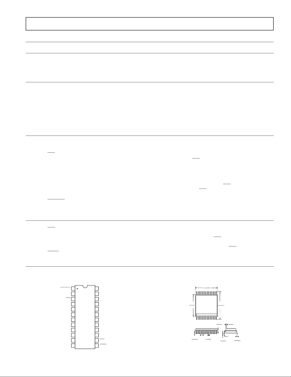
Dimensions shown in inches and (mm).
24-Pin Plastic DIP (N-24)
1.275 (32.30)
1.125 (28.60)
24
112
MAX
0.200 (5.05)
0.125 (3.18)
PIN 1
0.022 (0.558)
0.014 (0.356)
0.100
(2.54)
BSC
0.210
(5.33)
13
0.060 (1.52)
0.015 (0.38)
0.070 (1.77)
0.045 (1.15)
0.280 (7.11)
0.240 (6.10)
0.150
(3.81)
MIN
SEATING
PLANE
0.325 (8.25)
0.300 (7.62)
0.015 (0.381)
0.008 (0.204)
0.299 (7.6)
0.195 (4.95)
0.115 (2.93)
0.291 (7.39)
24-Pin Cerdip (Q-24)
28-Pin Plastic SOIC (R-28)
0.696 (17.67)
28 15
0.414 (10.52)
0.398 (10.10)
141
0.096 (2.44)
0.089 (2.26)
0.05
0.01 (0.254)
0.006 (0.15)
1. LEAD NO. 1 INDENTIFIED BY A DOT.
2. SOIC LEADS WILL BE EITHER TIN PLATED OR SOLDER DIPPED
IN ACCORDANCE WITH MIL-M-38510 REQUIREMENTS.
(1.27)
BSC
0.019 (0.49)
0.014 (0.35)
0.013 (0.32)
0.009 (0.23)
0.03 (0.76)
0.02 (0.51)
6°
0°
x 45°
0.042 (1.067
0.018 (0.457
C1472–10–11/90
PRINTED IN U.S.A.
–16–
REV. A
 Loading...