

Page 1
11-Bit Resolution
a
Simultaneous Sampling A/D Converter
FEATURES
11-Bit Resolution Analog-to-Digital Converter
Seven Single-Ended Analog Inputs
Four Input Channels Simultaneously Sampled
Expansion with 4 Multiplexed Inputs
Internal 2.5 V Reference
3.2 s Conversion Time per Channel
User Definable Channel Sequencing
Single Supply +5 V Operation
Double Buffered Register Outputs
6.25 MHz to 12.5 MHz Operating Clock Range
APPLICATIONS
Motor Control
3-Phase Power Measurement
Cellular Phones
Data Acquisition
GENERAL DESCRIPTION
The AD7861 is a multichannel simultaneous sampling A/D
Converter (ADC) configured for the acquisition of voltage
inputs in a motor control solution or three-phase power system.
The AD7861 combined with Analog Devices’ 16-bit fixedpoint digital signal processor (DSP) provides a low cost 16-bit
fixed-point microcontroller solution.
The input stage has been designed to accommodate the types of
signals frequently found in motor drives. The VIN1, VIN2, and
VIN3 channels are simultaneously sampled inputs suitable for
stator current acquisition. The AUX0–AUX3 channels are
multiplexed and are suitable for slower moving inputs such as
temperature and bus voltage of the diode rectifier output in a
motor control application.
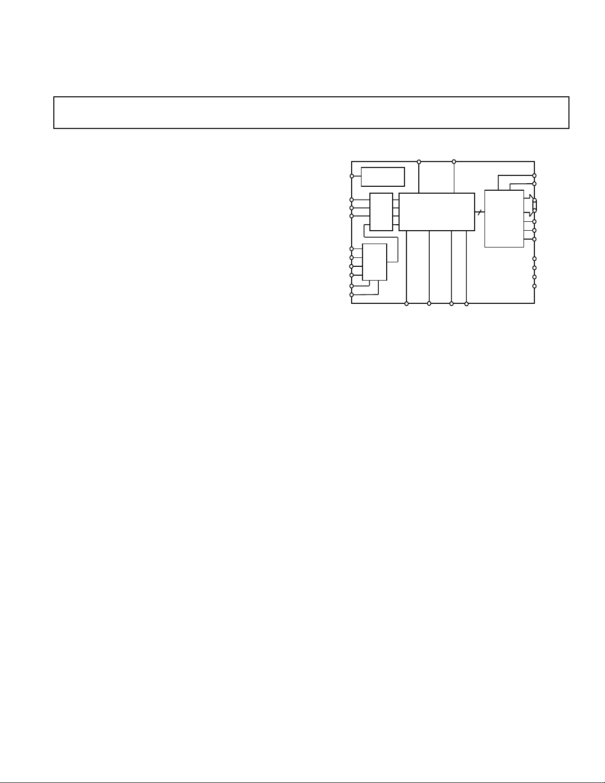
AD7861
FUNCTIONAL BLOCK DIAGRAM
REF IN
REF OUT
VIN1
VIN2
VIN3
AUX0
AUX1
AUX2
AUX3
S0
S1
2.5V
REFERENCE
SHA
4-1
MUX
CONVST
PRODUCT HIGHLIGHTS
Simultaneous Sampling of Four Inputs
Four channel sample and hold amplifier (SHA) allows out of
phase input signals to be sampled simultaneously, preserving
the relative phase information. Sample-and-hold acquisition
time is 1.6 µs and conversion time per channel is 3.2 µs (using
a 12.5 MHz system clock).
Flexible Analog Channel Sequencing
AD7861 supports acquisition of 2, 3 or 4 channels per group.
Converted channel results are stored in registers and the data
can be read in any order. The sampling and conversion time
for two channels is 8 µs, three channels is 11.2 µs, and four
channels is 14.4 µs (using a 12.5 MHz system clock).
Single 5 V dc Operation
Low power, digital process.
11-BIT
ADC
RESET
BUSY
M0 M1
12
OUTPUT
REGISTERS
AD7861
A0
A1
D0
D11
RD
CS
CLKIN
SGND
AGND
DGND
V
DD
REV. B
Information furnished by Analog Devices is believed to be accurate and
reliable. However, no responsibility is assumed by Analog Devices for its
use, nor for any infringements of patents or other rights of third parties
which may result from its use. No license is granted by implication or
otherwise under any patent or patent rights of Analog Devices.
One Technology Way, P.O. Box 9106, Norwood, MA 02062-9106, U.S.A.
Tel: 781/329-4700 World Wide Web Site: http://www.analog.com
Fax: 781/326-8703 © Analog Devices, Inc., 2000
Page 2

(VDD = 5 V ⴞ 5%; TA = –40ⴗC to +85ⴗC; REFIN = 2.5 V; Ext CLK @ 12.5 MHz, unless
AD7861–SPECIFICATIONS
otherwise noted)
Parameter AD7861AP Units Conditions/Comments
DC ACCURACY
Resolution 11 Bits Twos Complement Data Format
Relative Accuracy ± 2 LSB max Integral Nonlinearity
Differential Nonlinearity ± 2.5 LSB max
Bias Offset Error ± 9 LSB max Any Channel
Bias Offset Error Match 4 LSB max Between Channels
Full-Scale Error ± 13 LSB max Any Channel
Full-Scale Error Match 4 LSB max Between Channels
DYNAMIC PERFORMANCE
Signal-to-Noise Ratio (SNR) 60 dB min f
Total Harmonic Distortion (THD) –60 dB max f
Peak Harmonic or Spurious Noise –60 dB max f
= 1 kHz Sine Wave, f
IN
= 1 kHz Sine Wave, f
IN
= 1 kHz Sine Wave, f
IN
SAMPLE
SAMPLE
SAMPLE
= 75 kHz
= 75 kHz
= 75 kHz
Channel-to-Channel Isolation
M1 = 0 –58 dB max 1 kHz Sine Wave Applied to Unselected Channels
M1 = 1 –53 dB max 1 kHz Sine Wave Applied to Unselected Channels
REFERENCE
Input Voltage Range (REF IN) 2.5 V
Input Current 50 µA max
Onboard Reference Output (REF OUT) 2.5 V
Reference Tolerance ± 5%
Reference Drive Capability ± 100 µA max
SAMPLE-AND-HOLD
Acquisition Time 1.6 µs 20 CLK Cycles @ 12.5 MHz
Aperture Delay Time 200 ns max
Aperture Delay Time Match 20 ns max
Droop Rate 5 mV/ms max
LOGIC
Input High Voltage (V
Input Low Voltage (V
) 2 V min
IH
) 0.8 V max
IL
Input Leakage Current 1 µA max
Input Capacitance 20 pF typ
) 4.5 V min I
(V
OH
(V
) 0.4 V max I
OL
Current = 20 µA, VDD = 5 V
SOURCE
Current = 400 µA, VDD = 5 V
SINK
Three-State Leakage Current 1 µA max
CONVERSION RATE
Conversion Time/Channel 40 CLK Cycles
CONVST
Pulsewidth 2 CLK Cycles min
ANALOG INPUTS
Nominal Input Level 0–5 V VIN1, VIN2, VIN3, AUX0–AUX3
Input Current 100 µA
Input Capacitance 10 pF
SYSTEM CLOCK 6.25–12.5 MHz
POWER REQUIREMENTS
V
DD
I
DD
5V dc
10 mA max
– 2 –
REV. B
Page 3

AD7861
WARNING!
ESD SENSITIVE DEVICE
Table I. AD7861 Timing Parameters (TA = –4
0ⴗC to +85ⴗC and VDD = +5 V unless otherwise noted)
Number Symbol AD7861 Timing Requirements Min Max Units
1t
2t
3t
4t
5t
6t
7t
8t
9t
10 t
11 t
12 t
csb_rdb CS Low Before Falling Edge of RD 0–ns
su
addr_rdb ADDR Valid Before Falling Edge of RD 0–ns
su
rdb_data DATA Valid After Falling Edge of RD –25ns
dly
rdb RD Pulsewidth, Low 25 – ns
pwl
rdb RD Pulsewidth, High 25 – ns
pwh
rdb_data DATA Hold After Rising Edge of RD 10 – ns
hd
rdb_addr ADDR Hold After Rising Edge of RD 0–ns
hd
rdb_csb CS Hold After Rising Edge of RD 0–ns
hd
clk CLK Period 80 160 ns
per
clk CLK Pulsewidth, High 20 – ns
pwh
clk CLK Pulsewidth, Low 20 – ns
pwl
resetb RESET Pulsewidth, Low 2 × tperclk – ns
pwl
ABSOLUTE MAXIMUM RATINGS*
CLK
CS
A0–A1
RD
DATA
BUS
1, 2
7, 8
4
3
5
6
Supply Voltage (VDD) . . . . . . . . . . . . . . . . . . –0.3 V to +7.0 V
Digital Input Voltage . . . . . . . . . . . . . . . . . . . . . –0.3 V to V
Analog Input Voltage . . . . . . . . . . . . . . . . . . . . . –0.3 V to V
Analog Reference Input Voltage . . . . . . . . . . . –0.3 V to V
Digital Output Voltage Swing . . . . . . . . . . . . . . –0.3 V to V
Analog Reference Output Swing . . . . . . . . . . . –0.3 V to V
Operating Temperature . . . . . . . . . . . . . . . . . –40°C to +85°C
Lead Temperature (Soldering, 10 sec) . . . . . . . . . . . . +280°C
*
Stresses above those listed under Absolute Maximum Ratings may cause permanent damage to the device. This is a stress rating only; functional operation of the
device at these or any other conditions above those indicated in the operational
section of this specification is not implied. Exposure to absolute maximum rating
conditions for extended periods may affect device reliability.
Figure 1. Clock and Reset Timing
DD
DD
DD
DD
DD
9
10
CLK
11
ORDERING GUIDE
Model Temperature Range Package Option
CLK
12
RESET
AD7861AP –40°C to +85°C P-44A
Figure 2. Write Cycle Timing Diagram
CAUTION
ESD (electrostatic discharge) sensitive device. Electrostatic charges as high as 4000 V readily
accumulate on the human body and test equipment and can discharge without detection.
Although the AD7861 features proprietary ESD protection circuitry, permanent damage may
occur on devices subjected to high energy electrostatic discharges. Therefore, proper ESD
precautions are recommended to avoid performance degradation or loss of functionality.
REV. B
–3–
Page 4

AD7861
PIN DESCRIPTION
Pin Mnemonic Type Description
1 AUX0 I/P Auxiliary Input 0
2 REFIN I/P Analog Reference Input
3 AGND GND Analog Ground
4 REFOUT O/P Internal 2.5 Analog Reference
5 S0 I/P Aux Channel Select 0
6 S1 I/P Aux Channel Select 1
7 D0 O/P Data Bit 0 LSB (Tied Low)
8 D1 O/P Data Bit 1
9 D2 O/P Data Bit 2
10 D3 O/P Data Bit 3
11 D4 O/P Data Bit 4
12 D5 O/P Data Bit 5
13 D6 O/P Data Bit 6
14 D7 O/P Data Bit 7
15 D8 O/P Data Bit 8
16 D9 O/P Data Bit 9
17 D10 O/P Data Bit 10
18 D11 O/P Data Bit 11, MSB
19 DGND GND Logic Ground
20 DGND GND Logic Ground
21 V
DD
SUP +5 V Digital Supply
22 M0 I/P Conversion Mode Select 0
23 M1 I/P Conversion Mode Select 1
24 CONVST I/P A/D Conversion Start
25 CS I/P Chip Select
26 RD I/P Read Input
27 RESET I/P Chip Reset
28 A1 I/P Register Address Select 1
29 A0 I/P Register Address Select 0
30 NC NC No Connect
31 BUSY O/P Busy, Conversion in Process
32 CLK I/P External Clock Input 6.25 MHz-12.5 MHz
33–34 DGND GND Logic Ground
35 SGND GND Signal Ground
36 V
DD
SUP +5 V Analog Supply
37 VIN1 I/P Analog Input 1
38–39 NC NC No Connect
40 VIN2 I/P Analog Input 2
41 VIN3 I/P Analog Input 3
42 AUX3 I/P Auxiliary Input 3
43 AUX2 I/P Auxiliary Input 2
44 AUX1 I/P Auxiliary Input 1
PIN CONFIGURATION
AUX2
VIN3
AUX3
RD
CS
RESET
D0
7
D1
8
D2
9
D3
10
D4
11
D5
12
D6
13
14
D7
15
D8
16
D9
17
D10
NC = NO CONNECT
REFIN
AGND
REFOUT
S1
S0
AUX0
AUX1
2144345642414043
PIN 1
IDENTIFIER
AD7861
TOP VIEW
(Not to Scale)
181920 21 22 23 24 252627 28
DD
M1
DGND
M0
V
CONVST
D11
DGND
Pin Types Pin Types
I/P = Input Pin GND = Ground Pin
O/P = Output Pin SUP = Supply Pin
VIN2
A1
31
39
38
37
36
35
34
33
32
30
29
NC
NC
VIN1
V
DD
SGND
DGND
DGND
CLK
BUSY
NC
A0
–4–
REV. B
Page 5

AD7861
ANALOG INPUT BLOCK
The AD7861 is an 11-bit resolution, successive approximation
analog-to-digital (A/D) converter with twos complement output
data format. The analog input range is 0 V–5 V with a 2.5 V
reference as defined by the reference input pin (REFIN). The
AD7861 has an internal 2.5 V ± 5% reference, which is utilized
by connecting the reference output pin (REFOUT) to the
REFIN pin.
The A/D conversion time is determined by the system clock
frequency, which can range from 6.25 MHz to 12.5 MHz.
Forty clock cycles are required to complete each conversion.
There is a 4-channel simultaneous sample and hold amplifier
(SHA) at the AD7861 input stage. This allows up to 4 channels to
be simultaneously held and sequentially digitized. The SHA
acquisition time is 20 clock cycles and is independent of the
number of channels sampled.
The minimum throughput time can be calculated as follows:
tAA= t
where tAA = analog acquisition time, t
time, n = # channels, t
CONV
SHA
+ (n × t
)
CONV
= SHA acquisition
SHA
= conversion time per channel
(40 clock cycles).
A/D conversions are initiated by an external analog sample
clock pin (CONVST).
The CONVST input can be run asynchronous to the AD7861
system clock. When CONVST is run asynchronous from CLK,
the falling edge of CLK subsequent to CONVST high initiates
the conversion.
BUSY
The AD7861 BUSY pin goes low at the start of conversion, and
remains low for 40 clock cycles per channel. When BUSY goes
high, this indicates that the output data buffers have been
updated. Data from the previous conversion can be read up to
(n × 40 – 1) clock cycles after the start of conversion (n =
number of channels converted). Refer to Figure 3.
t
= (n x 40 –1) CLOCK CYCLES
t
= n x 40 CLOCK CYCLES
CLK
BUSY
t
= 1 CLOCK CYCLE
(n x 40 –1) CLOCK CYCLES
The user must select which channels to convert using M0/M1, a
minimum of two clock cycles before the start of conversion.
The AD7861 provides 4 auxiliary input channels which can be
individually multiplexed into the auxiliary ADC channel. Pins S0/
S1 are used to multiplex these auxiliary channels according to the
following table. It is important to note that the ADC performs a
series of conversions based on the input voltage on each pin
(including the AUX pin) at the start of the CONVST conversion
pulse. The user must select the auxiliary channel using S0/S1
a minimum of two clock cycles before the start of the conversion
sequence.
S1 S0 Channel Selected
0 0 AUX0
0 1 AUX1
1 0 AUX2
1 1 AUX3
DIGITAL INTERFACE
The AD7861 is designed to interface with the ADSP-21xx
family of DSPs. The 12-bit parallel interface can also be used
with other DSPs and microcontrollers.
The 11-bit A/D conversion output occupies the 11 most
significant bits of the 12-bit interface. The LSB (Data Bit 0) is
tied low.
REGISTER BASED INPUT/OUTPUT
To facilitate integration into most designs, a register based
input/output structure is provided. These registers can be
memory mapped into the user’s system along with other
memory mapped peripherals.
REGISTER ADDRESSING
Two address lines (A0 through A1) are used in conjunction with
control lines (CS, RD) to select registers VIN1, VIN2, VIN3, or
AUX. These control lines are active low. Timing and logical
sense is as for the ADSP-2100 family.
Pin Function
CS Enables the AD7861 Register Interface
RD Places the Internal Register on the Data Bus
CONVST
DATA
OLD DATA VALID NEW DATA VALID
Figure 3. Busy Pulse Timing
CHANNEL SELECTION
Determining which channels are converted is dependent on the
settings of M0 and M1. The available channel combinations are:
M1 M0 Channels Converted
0 0 VIN2, VIN3
0 1 VIN2, VIN3, AUX
1 0 VIN1, VIN2, VIN3
1 1 VIN1, VIN2, VIN3, AUX
REV. B
REGISTER LISTING
The output of each channel is stored in its respective register.
The symbolic names and address locations are listed in the
following table.
Name A1 A0 Register Function
VIN1 0 0 A/D Conversion Result Channel VIN1
VIN2 0 1 A/D Conversion Result Channel VIN2
VIN3 1 0 A/D Conversion Result Channel VIN3
AUX 1 1 A/D Conversion Result Channel AUX
–5–
Page 6

AD7861
DESCRIPTION OF THE REGISTERS
VIN1, VIN2, VIN3 These registers contain the results from
the conversion of the analog input voltages.
AUX In the AD7861, this register contains the
conversion result of the auxiliary channel
which had been selected by S0, S1.
Reading Results
The A/D conversion results for channels VIN1, VIN2, VIN3
and AUX are stored in the VIN1, VIN2, VIN3 and AUX
registers respectively. The twos complement data is left justified
and the LSB (Data Bit 0) is set to zero. The relationship
between input voltage and output coding is shown in Figure 4.
OUTPUT
011111111110
000000000000
100000000000
CODE
0V
FULL-SCALE
TRANSITION
FS = 5V
LSB =
2.5
INPUT VOLTAGE
5V
2048
5V-1LSB
Figure 4. AD7861 Transfer Function
Power Supply Connections and Setup
The nominal power supply level (VDD) is +5 V ± 5%. The
positive power supply (V
) should be connected to Pins 21
DD
and 36. The SGND and DGND pins should be star point
connected to AGND at a point close to the AD7861.
Power supplies should be bypassed at the power pins using a
0.1 µF capacitor. A 200 nF capacitor should also be connected
between REFIN and SGND.
DIGITAL SIGNAL PROCESSOR INTERFACING
The AD7861 A/D converter is designed to be easily interfaced
to Analog Devices’ family of Digital Signal Processors (DSPs).
Figure 5 shows the interface between the AD7861 and the
ADSP-2101/2105/2115 16-bit fixed point DSP, and the ADSP2171 and ADSP-2181 DSP Microcomputers. FLAGOUT from
the DSP is used to initiate the AD7861 conversion and is also
used in conjunction with the BUSY signal to provide an end of
conversion interrupt for the DSP. With M0 and M1 tied low,
the AD7861 is set up in the VIN2, VIN3 channel conversion
mode. By mapping the 12-bit AD7861 data bus into the top 12
bits of the DSP data bus (D12–D23), full-scale outputs from the
AD7861 can be represented as ±1.0 in fixed point arithmetic.
The AD7861 can operate with a clock frequency in the range of
6.25 MHz to 12.5 MHz. For the ADSP-2101/2105/2115 the
CLKOUT frequency is the system clock frequency. In the case
of the ADSP-2171/2181, the system clock is internally scaled, a
10 MHz system clock will result in a 20 MHz CLKOUT
frequency. If CLKOUT from the ADSP-2171/2181 is above
12.5 MHz, then an external clock divide down circuit will be
necessary.
ADDRESS BUS
CS
BUSY
CONVST
RD
CLK
M0
M1
A0–A1
AD7861
D0–D11*
A0–A13
ADSP-2101/
ADSP-2105/
ADSP-2115–12MHz
ADSP-2171–10MHz
ADSP-2181–10MHz
D0–D23
DMS
IRQ2
FLAGOUT
RD
CLKOUT
ADDRESS
DECODE
EN
DATA BUS
C2073a–1.5–3/00 (rev. B)
0.048 (1.21)
0.042 (1.07)
0.020
(0.50)
Figure 5. ADI Digital Signal Processor/Microcomputer
Interface
OUTLINE DIMENSIONS
Dimensions shown in inches and (mm).
44-Lead Plastic Leadless Chip Carrier
(P-44A)
0.180 (4.57)
0.165 (4.19)
PIN 1
IDENTIFIER
TOP VIEW
0.056 (1.42)
0.042 (1.07)
40
39
29
28
SQ
SQ
0.110 (2.79)
0.085 (2.16)
0.048 (1.21)
0.042 (1.07)
6
7
(PINS DOWN)
17
18
R
0.656 (16.66)
0.650 (16.51)
0.695 (17.65)
0.685 (17.40)
–6–
0.025 (0.63)
0.015 (0.38)
0.050
0.63 (16.00)
(1.27)
BSC
0.59 (14.99)
0.021 (0.53)
0.013 (0.33)
0.032 (0.81)
0.026 (0.66)
0.040 (1.01)
0.025 (0.64)
PRINTED IN U.S.A.
REV. B
 Loading...