

Page 1
LC2MOS
VDDV
FEATURES
16-bit monotonicity over temperature
±2 LSBs integral linearity error
Microprocessor compatible with readback capability
Unipolar or bipolar output
Multiplying capability
Low power (100 mW typical)
GENERAL DESCRIPTION
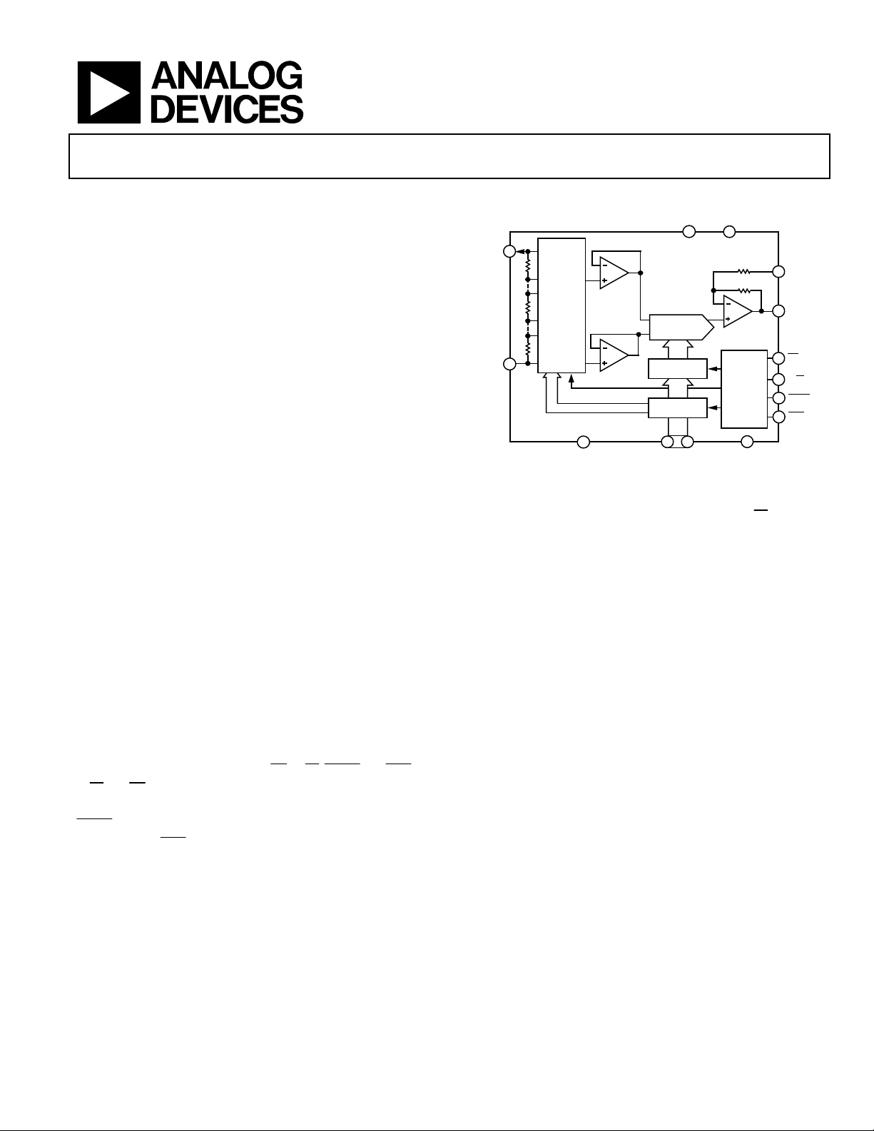
The AD7846 is a 16-bit DAC constructed with the Analog Devices,
2
Inc., LC
and an on-chip output amplifier. These can be configured to
give a unipolar output range (0 V to +5 V, 0 V to +10 V) or
bipolar output ranges (±5 V, ±10 V).
The DAC uses a segmented architecture. The four MSBs in the
DAC latch select one of the segments in a 16-resistor string.
Both taps of the segment are buffered by amplifiers and fed to a
12-bit DAC, which provides a further 12 bits of resolution. This
architecture ensures 16-bit monotonicity. Excellent integral
linearity results from tight matching between the input offset
voltages of the two buffer amplifiers.
In addition to the excellent accuracy specifications, the AD7846
also offers a comprehensive microprocessor interface. There are
16 data I/O pins, plus control lines (
R/
This is the readback function, which is useful in ATE applications.
LDAC
system and the
MOS process. It has V
W
and CS allow writing to and reading from the I/O latch.
REF+
and V
CS
reference inputs
REF−
LDAC
, R/W,
and
allows simultaneous updating of DACs in a multi-DAC
CLR
line will reset the contents of the DAC latch
CLR
).
16-Bit Voltage Output DAC
AD7846
FUNCTIONAL BLOCK DIAGRAM
CC
21 4
V
7
REF+
V
REF–
R
16
SEGMENT
R
SWITCH
MATRIX
R
8
4
A2
A1
9
V
SS
to 00…000 or 10…000 depending on the state of R/
means that the DAC output can be reset to 0 V in both the
unipolar and bipolar configurations.
The AD7846 is available in 28-lead plastic, ceramic, and PLCC
packages.
PRODUCT HIGHLIGHTS
1. 16-Bit Monotonicity
The guaranteed 16-bit monotonicity over temperature
makes the AD7846 ideal for closed-loop applications.
2. Readback
The ability to read back the DAC register contents
minimizes software routines when the AD7846 is used in
ATE systems.
3. Power Dissipation
Power dissipation of 100 mW makes the AD7846 the
lowest power, high accuracy DAC on the market.
AD7846
12-BIT DAC
DAC LATCH
I/O LATCH
10 3 20
DB15 DB0
Figure 1.
R
6
R
W
V
5
23
CS
22
R/W
25
LDAC
24
CLR
. This
IN
OUT
R
A3
12
12
CONTROL
LOGIC
DGND
08490-001
Rev. G
Information furnished by Analog Devices is believed to be accurate and reliable. However, no
responsibility is assumed by Analog Devices for its use, nor for any infringements of patents or other
rights of third parties that may result from its use. Specifications subject to change without notice. No
license is granted by implication or otherwise under any patent or patent rights of Analog Devices.
Trademarks and registered trademarks are the property of their respective owners.
One Technology Way, P.O. Box 9106, Norwood, MA 02062-9106, U.S.A.
Tel: 781.329.4700 www.analog.com
Fax: 781.461.3113 ©2000–2010 Analog Devices, Inc. All rights reserved.
Page 2

AD7846
TABLE OF CONTENTS
Features .............................................................................................. 1
Functional Block Diagram .............................................................. 1
General Description ......................................................................... 1
Product Highlights ........................................................................... 1
Revision History ............................................................................... 2
Specifications ..................................................................................... 3
AC Performance Characteristics ................................................ 4
Timing Characteristics ................................................................ 5
Absolute Maximum Ratings ............................................................ 6
ESD Caution .................................................................................. 6
Pin Configurations and Function Descriptions ........................... 7
Typical Performance Characteristics ............................................. 8
Terminology .................................................................................... 10
Circuit Description ......................................................................... 11
Digital Section ............................................................................. 11
Digital-to-Analog Conversion .................................................. 11
Output Stage ................................................................................ 12
Unipolar Binary Operation ........................................................... 13
Bipolar Operation ........................................................................... 14
Multiplying Operation ............................................................... 14
Position Measurement Application .............................................. 15
Microprocessor Interfacing ........................................................... 16
AD7846-to-8086 Interface ........................................................ 16
AD7846-to-MC68000 Interface ............................................... 16
Digital Feedthrough ....................................................................... 17
Application Hints ........................................................................... 18
Noise ............................................................................................ 18
Grounding ................................................................................... 18
Printed Circuit Board Layout ................................................... 18
Outline Dimensions ....................................................................... 20
Ordering Guide .......................................................................... 22
REVISION HISTORY
4/10—Rev. F to Rev. G
Change to Figure 1 ........................................................................... 1
12/09—Rev. E to Rev. F
Updated Format .................................................................. Universal
Changes to Table 4 ............................................................................ 6
Deleted Other Output Voltage Ranges Section ............................ 9
Deleted Figure 20 and Table 5; Renumbered Sequentially ......... 9
Deleted Test Application Section and Figure 21 ........................ 10
Deleted Figure 29 to Figure 31 ...................................................... 14
Changes to Printed Circuit Board Layout Section ..................... 18
Updated Outline Dimensions ....................................................... 20
Changes to Ordering Guide .......................................................... 22
Rev. G | Page 2 of 24
Page 3
AD7846
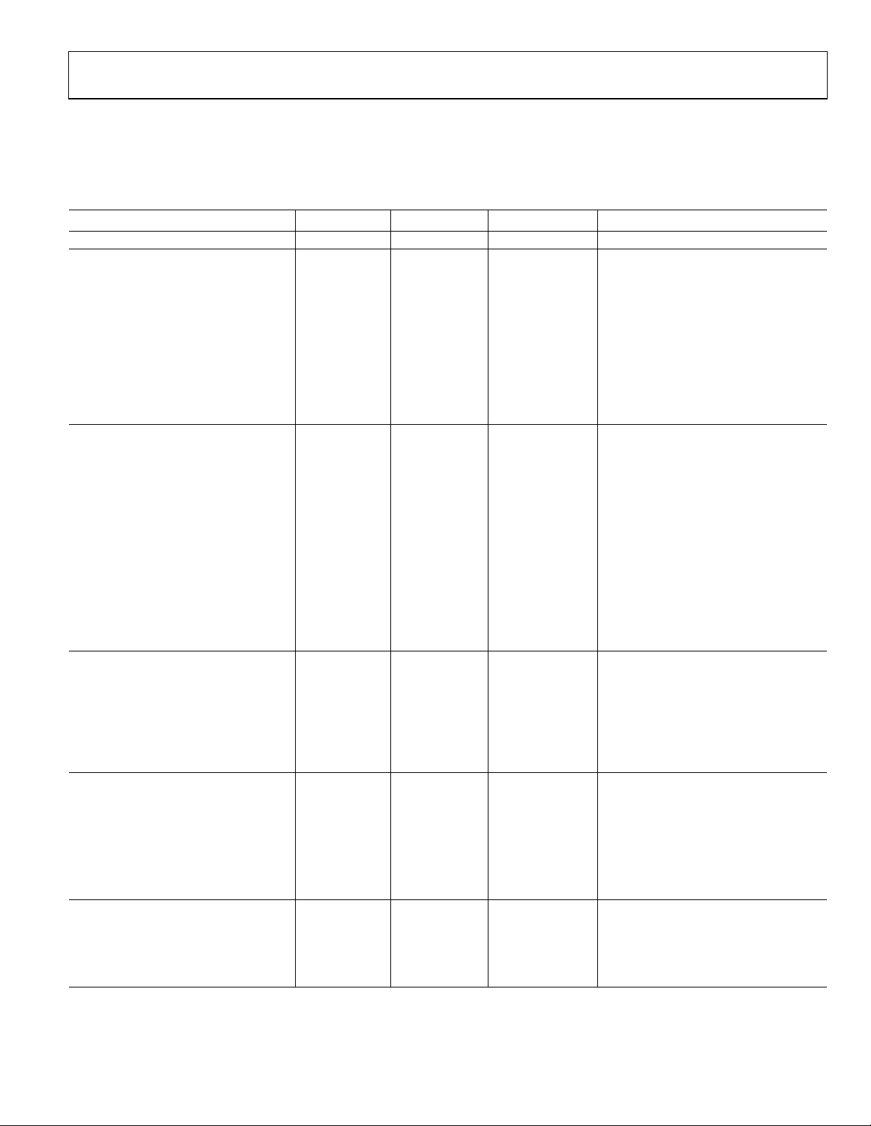
SPECIFICATIONS
VDD = +14.25 V to +15.75 V; VSS = −14.25 V to –15.75 V; VCC = +4.75 V to +5.25 V. V
R
connected to 0 V. All specifications T
IN
MIN
to T
, unless otherwise noted.
MAX
Table 1.
Parameter1 J, A Versions K, B Versions Unit Test Conditions/Comments
RESOLUTION 16 16 Bits
UNIPOLAR OUTPUT V
Relative Accuracy at +25°C ±12 ±4 LSB typ 1 LSB = 153 V
T
to T
MIN
±16 ±8 LSB max
MAX
Differential Nonlinearity Error ±1 ±0.5 LSB max All grades guaranteed monotonic
Gain Error at +25°C ±12 ±6 LSB typ V
T
to T
MIN
±16 ±16 LSB max
MAX
Offset Error at +25°C ±12 ±6 LSB typ
T
to T
MIN
±16 ±16 LSB max
MAX
Gain TC2 ±1 ±1 ppm FSR/°C typ
Offset TC2 ±1 ±1 ppm FSR/°C typ
BIPOLAR OUTPUT V
Relative Accuracy at +25°C ±6 ±2 LSB typ 1 LSB = 305 V
T
to T
MIN
±8 ±4 LSB max
MAX
Differential Nonlinearity Error ±1 ±0.5 LSB max All grades guaranteed monotonic
Gain Error at +25°C ±6 ±4 LSB typ V
T
to T
MIN
±16 ±16 LSB max
MAX
Offset Error at +25°C ±6 ±4 LSB typ V
T
to T
MIN
±16 ±12 LSB max
MAX
Bipolar Zero Error at +25°C ±6 ±4 LSB typ
T
to T
MIN
±12 ±8 LSB max
MAX
Gain TC2 ±1 ±1 ppm FSR/°Ctyp
Offset TC2 ±1 ±1 ppm FSR/°Ctyp
Bipolar Zero TC2 ±1 ±1 ppm FSR/°Ctyp
REFERENCE INPUT
Input Resistance 20 20 kΩ min Resistance from V
40 40 kΩ max Typically 30 kΩ
V
Range VSS + 6 to VSS + 6 to V min to
REF+
V
V
Range VSS + 6 to VSS + 6 to V min to
REF−
V
OUTPUT CHARACTERISTICS
Output Voltage Swing
− 6 VDD − 6 V max
DD
− 6 VDD − 6 V max
DD
V
+ 4 to VSS + 4 to
SS
V
− 3 VDD − 3
DD
V max
Resistive Load 2 2 kΩ min To 0 V
Capacitive Load 1000 1000 pF max To 0 V
Output Resistance 0.3 0.3 Ω typ
Short Circuit Current ±25 ±25 mA typ To 0 V or any power supply
DIGITAL INPUTS
VIH (Input High Voltage) 2.4 2.4 V min
VIL (Input Low Voltage) 0.8 0.8 V max
IIN (Input Current) ±10 ±10 A max
CIN (Input Capacitance)2 10 10 pF max
loaded with 2 kΩ, 1000 pF to 0 V; V
OUT
= 0 V, V
REF−
load = 10 MΩ
OUT
= –5 V, V
REF−
load = 10 MΩ
OUT
load = 10 MΩ
OUT
= 0 V to +10 V
OUT
= −10 V to +10 V
OUT
REF+
to V
REF+
REF−
= +5 V;
Rev. G | Page 3 of 24
Page 4
AD7846
Parameter1 J, A Versions K, B Versions Unit Test Conditions/Comments
DIGITAL OUTPUTS
VOL (Output Low Voltage) 0.4 0.4 V max I
VOH (Output High Voltage) 4.0 4.0 V min I
Floating State Leakage Current ±10 ±10 A max DB0 to DB15 = 0 to VCC
Floating State Output Capacitance2 10 10 pF max
POWER REQUIREMENTS3
VDD +11.4/+15.75 +11.4/+15.75 V min/V max
VSS −11.4/−15.75 −11.4/−15.75 V min/V max
VCC +4.75/+5.25 +4.75/+5.25 V min/V max
IDD 5 5 mA max V
ISS 5 5 mA max V
ICC 1 1 mA max
Power Supply Sensitivity4 1.5 1.5 LSB/V max
Power Dissipation 100 100 mW typ V
1
Temperature ranges as follows: J, K versions: 0°C to +70°C; A, B versions: −40°C to +85°C.
2
Guaranteed by design and characterization, not production tested.
3
The AD7846 is functional with power supplies of ±12 V. See the Typical Performance Characteristics section.
4
Sensitivity of gain error, offset error, and bipolar zero error to VDD, VSS variations.
AC PERFORMANCE CHARACTERISTICS
These characteristics are included for design guidance and are not subject to test. V
to −15.75 V; V
= +4.75 V to +5.25 V; RIN connected to 0 V, unless otherwise noted.
CC
= +5 V; VDD = +14.25 V to +15.75 V; VSS = −14.25 V
REF+
= 1.6 mA
SINK
= 400 A
SOURCE
unloaded
OUT
unloaded
OUT
unloaded
OUT
Table 2.
Parameter Limit at T
MIN
to T
(All Versions) Unit Test Conditions/Comments
MAX
Output Settling Time1 6 s max To 0.006% FSR, V
9 s max To 0.003% FSR, V
Slew Rate 7 V/s typ
Digital-to-Analog Glitch
Impulse 70 nV-sec typ
AC Feedthrough 0.5 mV p-p typ
DAC alternately loaded with 10…0000 and 01…1111,
V
unloaded
OUT
= 0 V, V
V
REF−
REF+
with all 0s
Digital Feedthrough 10 nV-sec typ
Output Noise Voltage
50 nV/√Hz typ
Density, 1 kHz to 100 kHz
1
LDAC
= 0. Settling time does not include deglitching time of 2.5 µs (typ).
DAC alternately loaded with all 1s and all 0s. CS
Measured at V
V
= V
REF+
REF−
OUT
= 0 V
loaded, V
OUT
loaded, V
OUT
= 0 V, typically 3.5 s
REF−
= –5 V, typically 6.5 s
REF−
= 1 V rms, 10 kHz sine wave, DAC loaded
high
, DAC loaded with 0111011…11,
Rev. G | Page 4 of 24
Page 5
AD7846
V
V
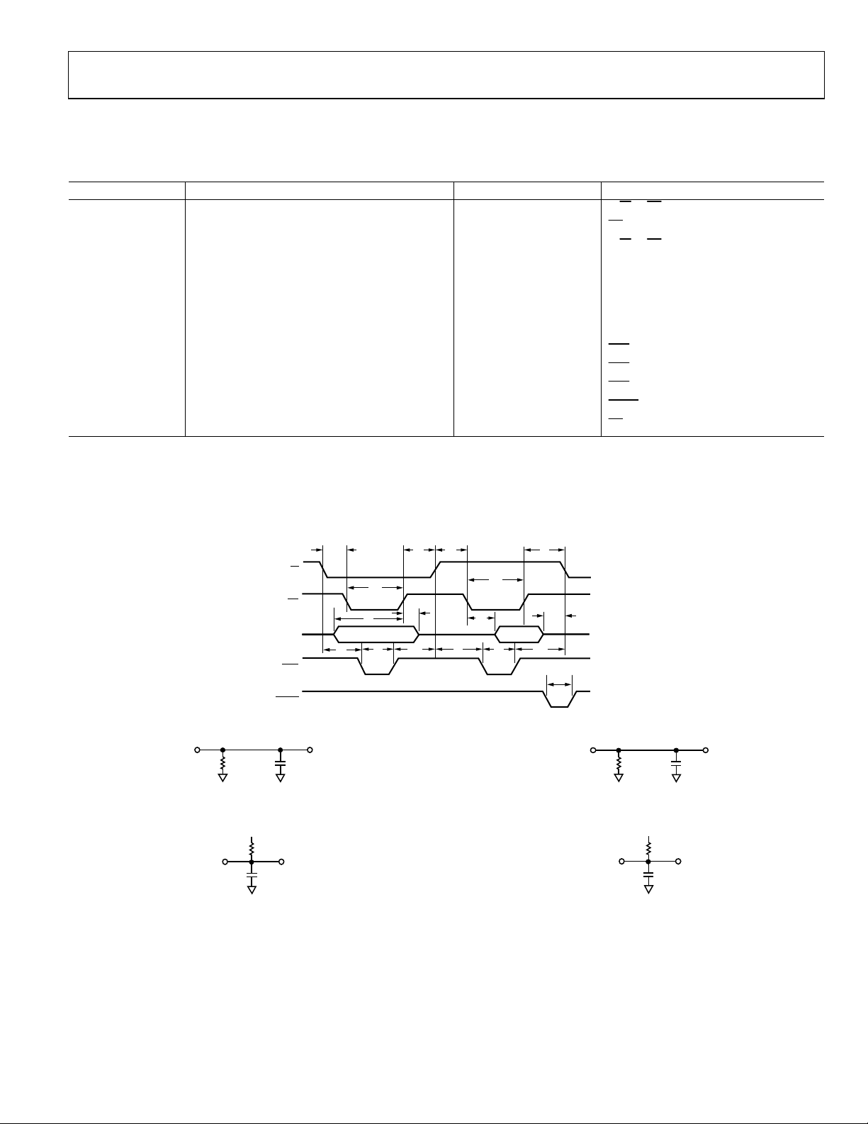
TIMING CHARACTERISTICS
VDD = +14.25 V to +15.75 V, VSS = −14.25 V to −15.75 V, VCC = +4.75 V to +5.25 V, unless otherwise noted.
Table 3.
Parameter1 Limit at T
t1
t2
t3
0 ns min
60 ns min
0 ns min
t4 60 ns min Data setup time
t5 0 ns min Data hold time
2
t
120 ns max Data access time
6
3
t
10 ns min Bus relinquish time
7
60 ns max
t8
t9
t10
t11
t12
1
Timing specifications are sample tested at +25°C to ensure compliance. All input control signals are specified with tR = tF = 5 ns (10% to 90% of +5 V) and timed from a
voltage level of 1.6 V.
2
t6 is measured with the load circuits of Figure 3 and Figure 4 and defined as the time required for an output to cross 0.8 V or 2.4 V.
3
t7 is defined as the time required for an output to change 0.5 V when loaded with the circuits of Figure 5 and Figure 6.
0 ns min
70 ns min
0 ns min
70 ns min
130 ns min
DBn
Figure 3. Load Circuit for Access Time (t
3kΩ
MIN
DGND
to T
(All Versions) Unit Test Conditions/Comments
MAX
to CS setup time
R/W
pulse width (write cycle)
CS
to CS hold time
R/W
setup time
CLR
pulse width
CLR
hold time
CLR
pulse width
LDAC
pulse width (read cycle)
CS
R/W
CS
DB0
TO
DB15
CLR
LDAC
t
1
t
t
4
t
8
t
3t1
t
2
t
5
t
t
10
9
12
t
6
t
t
8
t
3
t
DATA VALIDDATA VALID
t
10
9
5V
0V
5V
0V
7
5V
0V
5V
0V
t
11
5V
0V
8490-006
Figure 2. Timing Diagram
100pF
8490-002
)—High Z to VOH
6
Figure 5. Load Circuit for Access Time (t
DBn
3kΩ
DGND
10pF
08490-004
)—High Z to VOH
7
5
DBn
3kΩ
100pF
DGND
08490-003
Figure 4. Load Circuits for Bus Relinquish Time (t
)—High Z to V
6
DBn
OL
Figure 6. Load Circuits for Bus Relinquish Time (t
5
3kΩ
10pF
DGND
08490-005
7
)—High Z to V
OL
Rev. G | Page 5 of 24
Page 6
AD7846
ABSOLUTE MAXIMUM RATINGS
Table 4.
Parameter Rating
VDD to DGND −0.4 V to +17 V
VCC to DGND −0.4 V, VDD + 0.4 V, or +7 V
(whichever is lower)
VSS to DGND +0.4 V to −17 V
V
to DGND VDD + 0.4 V, VSS − 0.4 V
REF+
V
to DGND VDD + 0.4 V, VSS − 0.4 V
REF−
V
to DGND1 V
OUT
+ 0.4 V, VSS − 0.4 V, or ±10 V
DD
(whichever is lower)
RIN to DGND VDD + 0.4 V, VSS − 0.4 V
Digital Input Voltage to DGND −0.4 V to VCC + 0.4 V
Digital Output Voltage to DGND −0.4 V to VCC + 0.4 V
Power Dissipation (Any Package)
To +75°C 1000 mW
Derates above +75°C 10 mW/°C
Operating Temperature Range
J, K Versions 0°C to +70°C
A, B Versions −40°C to +85°C
Storage Temperature Range −65°C to +150°C
Lead Temperature (Soldering) +300°C
1
V
can be shorted to DGND, VDD, VSS, or VCC provided that the power
OUT
dissipation of the package is not exceeded.
Stresses above those listed under Absolute Maximum Ratings
may cause permanent damage to the device. This is a stress
rating only; functional operation of the device at these or any
other conditions above those indicated in the operational
section of this specification is not implied. Exposure to absolute
maximum rating conditions for extended periods may affect
device reliability.
ESD CAUTION
Rev. G | Page 6 of 24
Page 7
AD7846
V
V
PIN CONFIGURATIONS AND FUNCTION DESCRIPTIONS
VDDDB0
DB1
DB2
DB3
DB4
PIN 1
IDENTIFIER
DB9
DB8
DB5
DB7
25
24
23
22
21
20
19
LDAC
CLR
CS
R/W
V
CC
DGND
DB6
08490-008
DB2
DB1
DB0
V
V
OUT
R
REF+
REF–
V
DB15
DB14
DB13
DB12
DB11
DD
IN
SS
1
2
3
4
5
6
AD7846
7
TOP VIEW
(Not to Scale)
8
9
10
11
12
13
14
28
27
26
25
24
23
22
21
20
19
18
17
16
15
DB3
DB4
DB5
LDAC
CLR
CS
R/W
V
CC
DGND
DB6
DB7
DB8
DB9
DB10
V
V
REF+
V
REF–
DB15
DB14
08490-007
Figure 7. PDIP Pin Configuration
Table 5. Pin Function Descriptions
Pin Mnemonic Description
1 to 3 DB2 to DB0 Data I/Os. DB0 is LSB.
4 VDD Positive Supply for Analog Circuitry. This is +15 V nominal.
5 V
6 R
7 V
8 V
DAC Output Voltage.
OUT
Input to Summing Resistor of DAC Output Amplifier. This is used to select output voltage ranges. See Table 6.
IN
V
REF+
REF−
Input. The DAC is specified for V
REF+
Input. For unipolar operation connect V
V
REF−
REF+
= +5 V.
to 0 V, and for bipolar operation connect it to −5 V. The device is
REF−
specified for both conditions.
9 VSS Negative Supply for the Analog Circuitry. This is −15 V nominal.
10 to 19 DB15 to DB6 Data I/Os. DB15 is MSB.
20 DGND Ground for Digital Circuitry.
21 VCC Positive Supply for Digital Circuitry. This is +5 V nominal.
22
23
24
25
R/W Input. This pin can be used to load data to the DAC or to read back the DAC latch contents.
R/W
CS
CLR
LDAC
Chip Select Input. This pin selects the device.
Clear Input. The DAC can be cleared to 000…000 or 100…000. See Table 7.
Asynchronous Load Input to DAC.
26 to 28 DB5 to DB3 Data I/Os.
4 3 2 1 28 27 26
5
OUT
6
R
IN
7
8
9
V
SS
10
11
AD7846
TOP VIEW
(Not to Scale)
12 13 14 15 16 17 18
DB13
DB12
DB11
DB10
Figure 8. CERDIP Pin Configuration
Table 6. Output Voltage Ranges
Output Range V
0 V to +5 V +5 V 0 V V
V
REF+
R
REF−
IN
OUT
0 V to +10 V +5 V 0 V 0 V
+5 V to −5 V +5 V −5 V V
OUT
+5 V to −5 V +5 V 0 V +5 V
+10 V to −10 V +5 V −5 V 0 V
Rev. G | Page 7 of 24
Page 8
AD7846
TYPICAL PERFORMANCE CHARACTERISTICS
–0.40VA1
1V 2mV 20µs
Figure 9. AC Feedthrough, V
8
VDD = +15V
7
V
= –15V
SS
= +1V rms
+
V
REF
V
= 0V
–
6
REF
5
= 1 V rms, 10 kHz Sine Wave
REF+
08490-009
500
450
V
= V
REF–
= 0V
FREQUENCY (Hz)
REF+
GAIN = +1
400
DAC LOADED WIT H ALL 1s
350
300
250
200
150
100
NOISE SPECTRAL DENSITY (nV/√Hz)
50
0
100 1k 10k 100k 1M
Figure 12. Noise Spectral Density
V
OUT
50mV/DIV
08490-012
4
(mV p-p)
OUT
3
V
2
1
0
100
Figure 10. AC Feedthrough to V
30
VDD = +15V
V
SS
V
25
REF+
V
REF–
GAIN = +2
20
15
(V p-p)
OUT
V
10
5
0
10 100 1k 10k 100k 1M 10M
1k 10k 100k 1M
FREQUENCY (Hz)
vs. Frequency
OUT
= –15V
= ±5V SINE WAVE
= 0V
FREQUENCY (Hz)
DATA
0.5µs/DIV
08490-010
5V/DIV
8490-013
Figure 13. Digital-to-Analog Glitch Impulse Without Internal Deglitcher
(10…000 to 011…111 Transition)
V
OUT
LDAC
DATA
1µs/DIV
08490-011
50mV/DIV
5V/DIV
5V/DIV
8490-014
Figure 11. Large Signal Frequency Response
Figure 14. Digital-to-Analog Glitch Impulse with Internal Deglitcher
(10…000 to 011…111 Transition)
Rev. G | Page 8 of 24
Page 9

AD7846
0VA1
10V 5V 2µs
Figure 15. Pulse Response (Large Signal)
0.025VA1
100mV 50mV
Figure 16. Pulse Response (Small Signal)
REF 2.24V
10dB/DIV
V
, ±5V
+
REF
V
OUT
V
, ±50mV
+
REF
V
, ±100mV
+
OUT
1µs
RANGE 3.98V
, ±10V
+
MARKER 442.0Hz
1.70V
08490-015
08490-016
4.0
3.5
3.0
2.5
2.0
INL (LSB)
1.5
1.0
0.5
11 12 13 14 15
VDD, VSS (V)
TA = +25°C
V
= +5V
REF+
V
= 0V
REF–
GAIN = +1
16
8490-018
Figure 18. Typical Integral Nonlinearity vs. VDD/VSS
1.0
0.9
0.8
0.7
0.6
0.5
DNL (LSB)
0.4
0.3
0.2
0.1
0
11 12 13 14 15
VDD, VSS (V)
TA = +25°C
V
= +5V
REF+
V
= 0V
REF–
GAIN = +1
16
8490-019
Figure 19. Typical Differential Nonlinearity vs. VDD/VSS
START 100.0Hz
RBW 3Hz
VBW 10Hz
STOP 2000. 0Hz
Figure 17. Spectral Response of Digitally Constructed Sine Wave
ST 422 SEC
08490-017
Rev. G | Page 9 of 24
Page 10

AD7846
TERMINOLOGY
Least Significant Bit
This is the analog weighting of 1 bit of the digital word in a
− V
DAC. For the AD7846, 1 LSB = (V
REF+
REF−
)/216.
Relative Accuracy
Relative accuracy or endpoint nonlinearity is a measure of the
maximum deviation from a straight line passing through the
endpoints of the DAC transfer function. It is measured after
adjusting for both endpoints (that is, offset and gain errors are
adjusted out) and is normally expressed in least significant bits
or as a percentage of full-scale range.
Differential Nonlinearity
Differential nonlinearity is the difference between the measured
change and the ideal change between any two adjacent codes. A
specified differential nonlinearity of ±1 LSB over the operating
temperature range ensures monotonicity.
Gain Error
Gain error is a measure of the output error between an ideal
DAC and the actual device output with all 1s loaded after offset
error has been adjusted out. Gain error is adjustable to zero
with an external potentiometer.
Offset Error
This is the error present at the device output with all 0s loaded
in the DAC. It is due to op amp input offset voltage and bias
current and the DAC leakage current.
Bipolar Zero Error
When the AD7846 is connected for bipolar output and 10…000
is loaded to the DAC, the deviation of the analog output from
the ideal midscale of 0 V is called the bipolar zero error.
Digital-to-Analog Glitch Impulse
This is the amount of charge injected from the digital inputs to
the analog output when the inputs change state. This is normally
specified as the area of the glitch in either pA-sec or nV-sec
depending upon whether the glitch is measured as a current or
a voltage.
Multiplying Feedthrough Error
This is an ac error due to capacitive feedthrough from either of
the V
terminals to V
REF
when the DAC is loaded with all 0s.
OUT
Digital Feedthrough
When the DAC is not selected (that is,
CS
is held high), high
frequency logic activity on the digital inputs is capacitively
coupled through the device to show up as noise on the V
OUT
pin.
This noise is digital feedthrough.
Rev. G | Page 10 of 24
Page 11

AD7846
CIRCUIT DESCRIPTION
DIGITAL SECTION
Figure 20 shows the digital control logic and on-chip data latches
in the AD7846. Tab l e 7 is the associated truth table. The digitalto-analog converter (DAC) has two latches that are controlled
by four signals:
CS
connected to the data bus (DB15 to DB0). A word is written to
the input latch by bringing
of the input latch can be read back by bringing
high. This feature is called readback and is used in system
diagnostic and calibration routines.
Data is transferred from the input latch to the DAC latch with
LDAC
the
strobe. The equivalent analog value of the DAC latch
contents appears at the DAC output. The
DAC latch contents to 000…000 or 100…000, depending on the
state of R/
W
. Writing a
loads 100…000. To reset a DAC to 0 V in a unipolar system, the
user should assert
bipolar system, assert the
R/W
CLR
CS
, R/W,
LDAC
CS
CLR
, and
. The input latch is
low and R/W low. The contents
CS
CLR
pin resets the
CLR
loads 000…000 and reading a
CLR
while R/W is low; to reset to 0 V in a
CLR
while R/W is high.
DAC
16
DB15 RST
DB15 SET
DB14 TO DB0
RST
Figure 20. Input Control Logic
DB15 TO DB0
LATCHES
16
3-STATE I/O
LATCH
16
DB15 DB0
low and R/W
CLR
LDAC
08490-020
Table 7. Control Logic Truth Table
R/W
CS
LDAC CLR
Function
1 X X X 3-state DAC I/O latch in high-Z state
0 0 X X
DAC I/O latch loaded with DB15
to DB0
0 1 X X
Contents of DAC I/O latch available
on DB15 to DB0
X X 0 1
Contents of DAC I/O latch transferred
to DAC latch
X 0 X 0 DAC latch loaded with 000…000
X 1 X 0 DAC latch loaded with 100…000
DIGITAL-TO-ANALOG CONVERSION
Figure 21 shows the digital-to-analog section of the AD7846.
There are three DACs, each of which has its own buffer
amplifiers. DAC1 and DAC2 are 4-bit DACs. They share a
16-resistor string but have their own analog multiplexers. The
voltage reference is applied to the resistor string. DAC3 is a
12-bit voltage mode DAC with its own output stage.
The four MSBs of the 16-bit digital code drive DAC1 and DAC2,
and the 12 LSBs control DAC3. Using DAC1 and DAC2, the
MSBs select a pair of adjacent nodes on the resistor string and
present that voltage to the positive and negative inputs of
DAC3. This DAC interpolates between these two voltages to
produce the analog output voltage.
To prevent nonmonotonicity in the DAC due to amplifier offset
voltages, DAC1 and DAC2 leap along the resistor string. For
example, when switching from Segment 1 to Segment 2, DAC1
switches from the bottom of Segment 1 to the top of Segment 2
while DAC2 stays connected to the top of Segment 1. The code
driving DAC3 is automatically complemented to compensate
for the inversion of its inputs. This means that any linearity
effects due to amplifier offset voltages remain unchanged when
switching from one segment to the next and 16-bit monotonicity is
ensured if DAC3 is monotonic. Thus, 12-bit resistor matching
in DAC3 guarantees overall 16-bit monotonicity. This is much
more achievable than 16-bit matching, which a conventional
R-2R structure needs.
Rev. G | Page 11 of 24
Page 12

AD7846
V
V
REF+
DAC1
S1
S3
S15
S17
DB15 TO DB12 DB15 TO DB12
REF–
SEGMENT 16
DAC2
S2
S4
S14
S16
SEGMENT 1
Figure 21. Digital-to-Analog Conversion
OUTPUT STAGE
The output stage of the AD7846 is shown in Figure 22. It is capable
of driving a 2 kΩ/1000 pF load. It also has a resistor feedback
network that allows the user to configure it for gains of 1 or 2.
Tabl e 6 shows the different output ranges that are possible.
An additional feature is that the output buffer is configured as a
track-and-hold amplifier. Although normally tracking its input,
this amplifier is placed in a hold mode for approximately 2.5 µs
after the leading edge of
output at its previous voltage while the AD7846 is internally
changing to its new value. Thus, any glitches that occur in the
transition are not seen at the output. In systems where the
LDAC
is tied permanently low, the deglitching is not in
LDAC
. This short state keeps the DAC
R
DAC3
A1
12-BIT DAC
A2
operation. and show the outputs of the
DB11 TO DB0
Figure 13 Figure 14
R
A3
R
IN
V
OUT
08490-021
AD7846 without and with the deglitcher.
R
IN
10kΩ
DAC3
Figure 22. Output Stage
ONE
SHOT
LDAC
10kΩ
C1
V
OUT
08490-022
Rev. G | Page 12 of 24
Page 13

AD7846
V
V
UNIPOLAR BINARY OPERATION
Figure 23 shows the AD7846 in the unipolar binary circuit
configuration. The DAC is driven by the AD586 +5 V reference.
Because R
is tied to 0 V, the output amplifier has a gain of 2
IN
and the output range is 0 V to +10 V. If a 0 V to +5 V range is
required, R
should be tied to V
IN
, configuring the output
OUT
stage for a gain of 1. Tabl e 8 gives the code table for the circuit
of Figure 23.
1µF
+15
2
67
AD586
8
C1
4
SIGNAL
GROUND
R1
5
10kΩ
*ADDITIONAL PINS
OMITTE D FOR CLARITY
4
V
DD
V
REF+
AD7846*
8
V
REF–
Figure 23. Unipolar Binary Operation
V
–15V
+5
21
V
CC
V
DGND
SS
OUT
R
IN
5
6
20
V
OUT
(0V TO + 10V)
08490-023
Table 8. Code Table for Figure 23
Binary Number in DAC Latch
MSB LSB1 Analog Output (V
OUT
)
1111 1111 1111 1111 +10 (65,535/65,536) V
1000 0000 0000 0000 +10 (32,768/65,536) V
0000 0000 0000 0001 +10 (1/65,536) V
0000 0000 0000 0000 0 V
1
LSB = 10 V/216 = 10 V/65,536 = 152 µV.
Offset and gain can be adjusted in Figure 23 as follows:
• To adjust offset, disconnect the V
the DAC with all 0s, and adjust the V
input from 0 V, load
REF−
voltage until V
REF−
OUT
= 0 V.
• For gain adjustment, the AD7846 should be loaded with all
1s and R1 adjusted until V
= 10 (65,535)/(65,536) =
OUT
9.999847 V. If a simple resistor divider is used to vary the
V
voltage, it is important that the temperature
REF−
coefficients of these resistors match that of the DAC input
resistance (−300 ppm/°C). Otherwise, extra offset errors are
introduced over temperature. Many circuits do not require
these offset and gain adjustments. In these circuits, R1 can
be omitted. Pin 5 of the AD586 can be left open circuit and
Pin 8 (V
) of the AD7846 tied to 0 V.
REF−
Rev. G | Page 13 of 24
Page 14

AD7846
V+5V
Ω
*
V
BIPOLAR OPERATION
Figure 24 shows the AD7846 set up for ±10 V bipolar operation.
The AD588 provides precision ±5 V tracking outputs that are
fed to the V
REF+
and V
inputs of the AD7846. The code table
REF−
for Figure 24 is shown in Ta b le 9 .
+15
R1
39kΩ
46
AD588
2
3
1
14
15
16
13812
7
C1
1µF
9
R2
10k
100kΩ
ADDITIONAL PINS OMI TTED FO R CLARITY
5
10
11
R3
Figure 24. Bipolar ±10 V Operation
+15V
–15V
+15
V
7
REF+
8
V
REF–
4
V
V
DD
V
AD7846*
DGND
V
SS
9
–15V
21
CC
OUT
R
IN
V
5
OUT
(–10V TO +10V)
6
20
SIGNAL
GROUND
Table 9. Offset Binary Code Table for Figure 24
Binary Number in DAC Latch
MSB LSB1
Analog Output (V
OUT
)
1111 1111 1111 1111 +10 (32,767/32,768) V
1000 0000 0000 0001 +10 (1/32,768) V
1000 0000 0000 0000 0 V
0111 1111 1111 1111 −10 (1/32,768) V
0000 0000 0000 0000 −10 (32,768/32,768) V
1
LSB = 10 V/215 = 10 V/32,768 = 305 V.
8490-024
Full-scale and bipolar zero adjustment are provided by varying
the gain and balance on the AD588. R2 varies the gain on the
AD588 while R3 adjusts the +5 V and −5 V outputs together
with respect to ground.
For bipolar zero adjustment on the AD7846, load the DAC with
100…000 and adjust R3 until V
by loading the DAC with all 1s and adjusting R2 until V
= 0 V. Full scale is adjusted
OUT
OUT
=
9.999694 V.
When bipolar zero and full-scale adjustment are not needed, R2
and R3 can be omitted, Pin 12 on the AD588 should be connected
to Pin 11, and Pin 5 should be left floating. If a user wants a 5 V
output range, there are two choices. By tying Pin 6 (R
AD7846 to V
(Pin 5), the output stage gain is reduced to
OUT
) of the
IN
unity and the output range is ±5 V. If only a positive 5 V reference
is available, bipolar ±5 V operation is still possible. Tie V
0 V and connect R
IN
to V
. This also gives a ±5 V output
REF+
REF−
to
range. However, the linearity, gain, and offset error specifications
are the same as the unipolar 0 V to 5 V range.
MULTIPLYING OPERATION
The AD7846 is a full multiplying DAC. To obtain four-quadrant
multiplication, tie V
tie R
IN
to V
. Figure 11 shows the large signal frequency
REF+
to 0 V, apply the ac input to V
REF−
response when the DAC is used in this fashion.
REF+
, and
Rev. G | Page 14 of 24
Page 15

AD7846
A
POSITION MEASUREMENT APPLICATION
Figure 25 shows the AD7846 in a position measurement application using an linear variable displacement transducer (LVDT),
an AD630 synchronous demodulator and a comparator to make
a 16-bit LVDT-to-digital converter. The LVDT is excited with a
fixed frequency and fixed amplitude sine wave (usually 2.5 kHz,
2 V p-p). The outputs of the secondary coil are in antiphase and
their relative amplitudes depend on the position of the core in the
LVDT. The AD7846 output interpolates between these two inputs
in response to the DAC input code. The AD630 is set up so that
it rectifies the DAC output signal. Thus, if the output of the DAC is
in phase with the V
tor is positive, and if it is in phase with V
tive. By turning on each bit of the DAC in succession starting
with the MSB and deciding to leave it on or turn it off based on
the comparator output, a 16-bit measurement of the core position
is obtained.
input, the inverting input to the compara-
REF+
, the output is nega-
REF−
SIN ω t
*ADDITIONAL PINS OMITTED FOR CLARITY
LVDT
–(1–x) ASIN ω t
x ASIN ω t
R1
100kΩ
C1
1µF
Figure 25. AD7846 in Position Measurement Application
V
OUT
V
7
REF+
R
IN
AD7846*
8
V
REF–
10
9
10
AD630*
13
20
DGND
DB0DB15
3
PROCESSOR DATA BUS
16
TO
PROCESSOR PORT
5
6
SIGNAL
GROUND
08490-027
Rev. G | Page 15 of 24
Page 16

AD7846
1
a
$
#
*
MICROPROCESSOR INTERFACING
AD7846-TO-8086 INTERFACE
Figure 26 shows the 8086 16-bit processor interfacing to the
AD7846. The double buffering feature of the DAC is not used in
this circuit because
AD15 (the 16-bit data bus) are connected to the DAC data bus
(DB0 to DB15). The 16-bit word is written to the DAC in one
MOV instruction and the analog output responds immediately.
In this example, the DAC address is 0xD000.
ALE
8086
DEN
RD
WR
AD0 TO AD15
*LINEAR CIRCUIT RY OMITTED FOR CLARI TY
In a multiple DAC system, the double buffering of the AD7846
allows the user to simultaneously update all DACs. In Figure 27,
a 16-bit word is loaded to the input latches of each of the DACs
in sequence. Then, with one instruction to the appropriate
address,
CS4
DACs simultaneously.
LDAC
is permanently tied to 0 V. AD0 to
ADDRESS BUS
ADDRESS
16-BIT
LATCH
DATA BUS
DECODE
+5V
Figure 26. AD7846-to-8086 Interface Circuit
(that is,
LDAC
) is brought low, updating all the
ADDRESS BUS
CS
LDAC
CLR
AD7846*
R/W
DB0 TO DB15
08490-028
AD7846-TO-MC68000 INTERFACE
Interfacing between the AD7846 and MC68000 is accomplished
using the circuit of Figure 28. The following routine writes data
to the DAC latches and then outputs the data via the DAC latch.
000 MOVE.W
MOVE.W
MOVE.W
TRAP
A1 TO A23
MC68000
DS
DTACK
R/W
D0 TO D15 DB0 TO DB15
#W,
D0
D0,
E000
228,
D7
#14
ADDRESS BUS
ADDRESS
DECODE
DATA BUS
The desired DAC dat
W, is loaded into
Data Register 0. W
may be any value
between 0 and 65535
(decimal) or 0 and
FFFF (hexadecimal).
The data, W, is
transferred between
D0 and the DAC
register.
Control is returned
to the System Monitor
using these two
instructions.
CS
+5V
CLR
LDAC
AD7846*
R/W
,
ADDRESS
16-BIT
ALE
8086
AD0 TO AD15
*LINEAR CI RCUITRY OMIT TED FO R CLARIT Y
LATCH
DEN
RD
WR
DATA BUS
DECODE
Figure 27. AD7846-to-8086 Interface: Multiple DAC System
CS
LDAC
AD7846*
R/W
CLR
DB0 TO DB15
CS
AD7846*
LDAC
R/W
CLR
DB0 TO DB15
CS
AD7846*
LDAC
R/W
CLR
DB0 TO DB15
+5V
+5V
+5V
08490-029
Rev. G | Page 16 of 24
LINEAR CIRCUIT RY OMIT TED FOR CLARITY
Figure 28. AD7846-to-MC68000 Interface
8490-030
Page 17

AD7846
DIGITAL FEEDTHROUGH
In the preceding interface configurations, most digital inputs to
the AD7846 are directly connected to the microprocessor bus.
Even when the device is not selected, these inputs are constantly
changing. The high frequency logic activity on the bus can feed
through the DAC package capacitance to show up as noise on
the analog output. To minimize this digital feedthrough, isolate
the DAC from the noise source. Figure 29 shows an interface
circuit that isolates the DAC from the bus.
Note that to make use of the AD7846 readback feature using
the isolation technique of Figure 29, the latch needs to be
bidirectional.
A1 TO A15
MICRO-
PROCESSOR
R/W R/W
D0 TO D15 DB0 TO DB15
*LINEAR CIRCUIT RY OMITTED FOR CLARI TY
ADDRESS BUS
ADDRESS
DECODE
DATA BUS
DIR G
B BUS A BUS
2×
74LS245
+5V
CS
CLR
LDAC
AD7846*
08490-031
Figure 29. AD7846 Interface Circuit Using Latches to Minimize Digital Feedthrough
Rev. G | Page 17 of 24
Page 18

AD7846
*
Y
APPLICATION HINTS
NOISE
In high resolution systems, noise is often the limiting factor.
With a 10 V span, a 16-bit LSB is 152 V (–96 dB). Thus, the
noise floor must stay below −96 dB in the frequency range of
interest. Figure 12 shows the noise spectral density for the
AD7846.
GROUNDING
As well as noise, the other prime consideration in high resolution
DAC systems is grounding. With an LSB size of 152 V and a
load current of 5 mA, 1 LSB of error can be introduced by series
resistance of only 0.03 .
Figure 30 shows recommended grounding for the AD7846 in a
typical application.
ANALOG SUPPLY DIGIT AL SUPPLY
SIGNAL
GROUND
ADDITIONAL PI NS OMITT ED FOR CLARIT
–15V+15V 0V DGND+5V
R1
2 9 16 4 9 21 20
R2
1
7
AD588*
3
R3
15
14
R5
Figure 30. AD7846 Grounding
AD7846*
8
6
R4
V
R
L
OUT
(+5V TO –5V)
5
08490-032
R1 to R5 represent lead and track resistances on the printed
circuit board. R1 is the resistance between the analog power
supply ground and the signal ground. Because current flowing
in R1 is very low (bias current of AD588 sense amplifier), the
effect of R1 is negligible. R2 and R3 represent track resistance
between the AD588 outputs and the AD7846 reference inputs.
Because of the force and sense outputs on the AD588, these
resistances will also have a negligible effect on accuracy.
R4 is the resistance between the DAC output and the load. If R
is constant, then R4 introduces a gain error only that can be
trimmed out in the calibration cycle. R5 is the resistance
between the load and the analog common. If the output voltage
is sensed across the load, R5 introduces a further gain error,
which can be trimmed out. If, on the other hand, the output
voltage is sensed at the analog supply common, R5 appears as
part of the load and therefore introduces no errors.
PRINTED CIRCUIT BOARD LAYOUT
Figure 31 shows the AD7846 in a typical application with the
AD588 reference, producing an output analog voltage in the
±10 V range. Full-scale and bipolar zero adjustment are
provided by Potentiometer R2 and Potentiometer R3. Latches
(2 × 74LS245) isolate the DAC digital inputs from the active
microprocessor bus and minimize digital feedthrough.
L
Rev. G | Page 18 of 24
Page 19

AD7846
V
C1
10µF
R1
R2
100kΩ
C12
1µF
R3
100kΩ
39kΩ
7
AD588
5
10
11
12
813 9
C2
0.1µF
264
3
1
14
15
16
0.1µF
(+10V TO –10V)
–15V
C4
V
OUT
C3
10µF
7
8
9
20
6
5
+15
V
REF+
AD7846
V
REF–
V
SS
DGND
R
IN
V
OUT
214
DB15
DB14
DB13
DB12
DB11
DB10
DB9
DB8
DB7
DB6
DB5
DB4
DB3
DB2
DB1
DB0
R/W
CS
CLR
LDAC
C31/A31
C4/A4
C5/A5
C6/A6
C7/A7
C8/A8
C9/A9
C10/A10
C11/A11
C12/A12
C13/A13
C14/A14
C15/A15
C16/A16
C17/A17
C18/A18
C19/A19
C20/A20
C21/A21
C22/A22
C23/A23
C32/A32
J1
08490-033
C5
10µF
10
11
12
13
14
15
16
17
18
19
26
27
28
1
2
3
22
23
24
25
C6
0.1µF
2
3
4
5
6
7
8
9
2
3
4
5
6
7
8
9
10
10
74LS245
119
+5V
74LS245
119
+5V
C7
0.1µF
20
18
17
16
15
14
13
12
11
20
18
17
16
15
14
13
12
11
Figure 31. Schematic for AD7846 Board
Rev. G | Page 19 of 24
Page 20

AD7846
OUTLINE DIMENSIONS
0.005 (0.13)
MIN
28
114
PIN 1
0.225(5.72)
MAX
0.200 (5.08)
0.125 (3.18)
0.026 (0.66)
0.014 (0.36)
1.490 (37.85) MAX
CONTROLL ING DIMENS IONS ARE IN INCHES; MILLIMETER DI MENSIONS
(IN PARENTHESES) ARE ROUNDED-OF F INCH EQUI VALENTS FOR
REFERENCE ONLY AND ARE NOT APPROPRI ATE FOR USE IN DES IGN.
Figure 32. 28-Lead Ceramic Dual In-Line Package [CERDIP]
1.565 (39.75)
1.380 (35.05)
28
114
0.100 (2.54)
0.250 (6.35)
0.200 (5.08)
0.115 (2.92)
0.022 (0.56)
0.014 (0.36)
MAX
BSC
0.070 (1.78)
0.050 (1.27)
0.100 (2.54)
MAX
15
0.610 (15.49)
0.500 (12.70)
0.015 (0.38)
MIN
0.150 (3.81)
MIN
15°
0.100
(2.54)
BSC
0.070 (1.78)
0.030 (0.76)
SEATING
PLANE
0°
(Q-28-2)
Dimensions shown in inches and (millimeters)
15
0.580 (14.73)
0.485 (12.31)
0.015 (0.38)
GAUGE
PLANE
0.015
(0.38)
MIN
SEATING
PLANE
0.005 (0.13)
MIN
0.625 (15.88)
0.600 (15.24)
0.700 (17.78)
MAX
0.620 (15.75)
0.590 (14.99)
0.018 (0.46)
0.008 (0.20)
0.015 (0.38)
0.008 (0.20)
0.195 (4.95)
0.125 (3.17)
030106-A
CONTROLL ING DIMENSIONS ARE IN INCHES; MIL LIMETER DIMENSIONS
(IN PARENTHESES) ARE ROUNDED-O FF INCH EQ UIVALENTS FOR
REFERENCE ON LY AND ARE NOT APPROPRI ATE FOR USE IN DESIGN.
CORNER LEADS M AY BE CONFIGURED AS WHOLE LEADS.
COMPLIANT TO JEDEC STANDARDS MS-011
Figure 33. 28-Lead Plastic Dual In-Line Package [PDIP]
Wide Body
(N-28-2)
Dimensions shown in inches and (millimeters)
Rev. G | Page 20 of 24
071006-A
Page 21

AD7846
0.458 (11.63)
0.442 (11.23)
0.100 (2.54)
0.064 (1.63)
0.458
(11.63)
SQ
MAX
SQ
0.088 (2.24)
0.054 (1.37)
CONTROLLING DIMENSIONS ARE IN INCHES; MILLIMETER DIMENSIONS
(IN PARENTHESES) ARE ROUNDED-OFF INCH EQUIVALENTS FOR
REFERENCE ONLY AND ARE NOT APPROPRIATE FOR USE IN DESIGN
0.05 (1.27)
0.075 (1.91)
REF
0.055 (1.40)
0.045 (1.14)
0.075
(1.91)
REF
19 25
11
18
BOTTON
VIEW
26
28
1
412
0.300 (7.62)
REF
0.020 (0.51)
MIN
0.028 (0.71)
0.022 (0.56)
0.15 (3.81)
REF
5
0.095 (2.41)
0.075 (1.90)
022106-A
Figure 34. 28-Terminal Ceramic Leadless Chip Carrier [LCC]
(E-28-1)
Dimensions shown in inches and (millimeters)
0.180 (4.57)
0.120 (3.04)
0.090 (2.29)
0.165 (4.19)
0.020 (0.51)
MIN
0.021 (0.53)
0.013 (0.33)
0.032 (0.81)
0.026 (0.66)
0.045 (1.14)
0.025 (0.64)
0.430 (10.92)
0.390 (9.91)
R
BOTTOM
VIEW
(PINS UP)
042508-A
0.048 (1.22)
0.042 (1.07)
0.048 (1.22)
0.042 (1.07)
4
5
11
12
0.456 (11.582)
0.450 (11.430)
0.495 (12.57)
0.485 (12.32)
0.056 (1.42)
0.042 (1.07)
26
25
PIN 1
IDENTIFIER
TOP VIEW
(PINS DOWN)
CONTROLL ING DIMENS IONS ARE IN I NCHES; MILL IMETER DI MENSIONS
(IN PARENTHESES ) ARE ROUNDED-OF F INCH EQUI VALENTS FOR
REFERENCE ONLY AND ARE NOT APPROPRIATE FO R USE IN DESIGN.
0.050
(1.27)
BSC
19
18
SQ
SQ
COMPLIANT TO JEDEC STANDARDS MO-047-AB
Figure 35. 28-Lead Plastic Leaded Chip Carrier [PLCC]
(P-28)
Dimensions shown in inches and (millimeters)
Rev. G | Page 21 of 24
Page 22

AD7846
ORDERING GUIDE
Model1 Temperature Range Relative Accuracy Package Description Package Option
5962-89697013A −55°C to +125°C ±16 LSB 28-Terminal Ceramic Leadless Chip Carrier [LCC] E-28-1
5962-8969701XA −55°C to +125°C ±16 LSB 28-Lead Ceramic Dual In-Line Package [CERDIP] Q-28-2
AD7846JN 0°C to +70°C ±16 LSB 28-Lead Plastic Dual In-Line Package [PDIP] N-28-2
AD7846JNZ 0°C to +70°C ±16 LSB 28-Lead Plastic Dual In-Line Package [PDIP] N-28-2
AD7846KN 0°C to +70°C ±8 LSB 28-Lead Plastic Dual In-Line Package [PDIP] N-28-2
AD7846KNZ 0°C to +70°C ±8 LSB 28-Lead Plastic Dual In-Line Package [PDIP] N-28-2
AD7846JP 0°C to +70°C ±16 LSB 28-Lead Plastic Leaded Chip Carrier [PLCC] P-28
AD7846JP-REEL 0°C to +70°C ±16 LSB 28-Lead Plastic Leaded Chip Carrier [PLCC] P-28
AD7846JPZ 0°C to +70°C ±16 LSB 28-Lead Plastic Leaded Chip Carrier [PLCC] P-28
AD7846JPZ-REEL 0°C to +70°C ±16 LSB 28-Lead Plastic Leaded Chip Carrier [PLCC] P-28
AD7846KP 0°C to +70°C ±8 LSB 28-Lead Plastic Leaded Chip Carrier [PLCC] P-28
AD7846KP-REEL 0°C to +70°C ±8 LSB 28-Lead Plastic Leaded Chip Carrier [PLCC] P-28
AD7846KPZ 0°C to +70°C ±8 LSB 28-Lead Plastic Leaded Chip Carrier [PLCC] P-28
AD7846KPZ-REEL 0°C to +70°C ±8 LSB 28-Lead Plastic Leaded Chip Carrier [PLCC] P-28
AD7846AP −40°C to +85°C ±16 LSB 28-Lead Plastic Leaded Chip Carrier [PLCC] P-28
AD7846APZ −40°C to +85°C ±16 LSB 28-Lead Plastic Leaded Chip Carrier [PLCC] P-28
AD7846AQ −40°C to +85°C ±16 LSB 28-Lead Ceramic Dual In-Line Package [CERDIP] Q-28-2
AD7846BP −40°C to +85°C ±8 LSB 28-Lead Plastic Leaded Chip Carrier [PLCC] P-28
AD7846BPZ −40°C to +85°C ±8 LSB 28-Lead Plastic Leaded Chip Carrier [PLCC] P-28
AD7846ACHIPS −40°C to +85°C ±16 LSB DIE
1
Z = RoHS Compliant Part.
Rev. G | Page 22 of 24
Page 23

AD7846
NOTES
Rev. G | Page 23 of 24
Page 24

AD7846
NOTES
©2000–2010 Analog Devices, Inc. All rights reserved. Trademarks and
registered trademarks are the property of their respective owners.
D08490-0-4/10(G)
Rev. G | Page 24 of 24
 Loading...