

Page 1
LC2MOS
a
FEATURES
12-Bit CMOS MDAC with Output Amplifier
4-Quadrant Multiplication
Guaranteed Monotonic (T
Space-Saving 0.3" DIPs and 24- or 28-Terminal Surface
Mount Packages
Application Resistors On Chip for Gain Ranging, etc.
Low Power LC
APPLICATIONS
Automatic Test Equipment
Digital Attenuators
Programmable Power Supplies
Programmable Gain Amplifiers
Digital-to-4–20 mA Converters
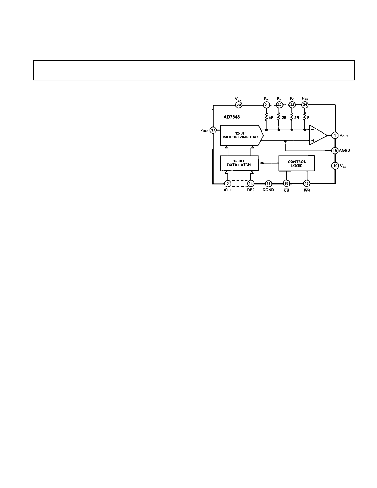
GENERAL DESCRIPTION
The AD7845 is the industry’s first 4-quadrant multiplying D/A
converter with an on-chip amplifier. It is fabricated on the
2
MOS process, which allows precision linear components
LC
and digital circuitry to be implemented on the same chip.
The 12 data inputs drive latches which are controlled by standard CS and WR signals, making microprocessor interfacing
simple. For stand-alone operation, the CS and WR inputs can
be tied to ground, making all latches transparent. All digital
inputs are TTL and 5 V CMOS compatible.
The output amplifier can supply ±10 V into a 2 kΩ load. It is
internally compensated, and its input offset voltage is low due to
laser trimming at wafer level. For normal operation, R
to V
scale the output voltage range.
, but the user may alternatively choose RA, RB or RC to
OUT
2
MOS
MIN
to T
MAX
)
is tied
FB
Complete 12-Bit Multiplying DAC
AD7845
FUNCTIONAL BLOCK DIAGRAM
PRODUCT HIGHLIGHTS
1. Voltage Output Multiplying DAC
The AD7845 is the first DAC which has a full 4-quadrant
multiplying capability and an output amplifier on chip. All
specifications include amplifier performance.
2. Matched Application Resistors
Three application resistors provide an easy facility for gain
ranging, voltage offsetting, etc.
3. Space Saving
The AD7845 saves space in two ways. The integration of the
output amplifier on chip means that chip count is reduced.
The part is housed in skinny 24-lead 0.3" DIP, 28-terminal
LCC and PLCC and 24-terminal SOIC packages.
REV. B
Information furnished by Analog Devices is believed to be accurate and
reliable. However, no responsibility is assumed by Analog Devices for its
use, nor for any infringements of patents or other rights of third parties
which may result from its use. No license is granted by implication or
otherwise under any patent or patent rights of Analog Devices.
One Technology Way, P.O. Box 9106, Norwood, MA 02062-9106, U.S.A.
Tel: 781/329-4700 World Wide Web Site: http://www.analog.com
Fax: 781/326-8703 © Analog Devices, Inc., 1999
Page 2
1
AD7845–SPECIFICATIONS
V
connected to RFB. V
OUT
load = 2 k⍀, 100 pF. All specifications T
OUT
(VDD = +15 V, ⴞ 5%, VSS = –15 V, ⴞ 5%, V
to T
MIN
unless otherwise noted.)
MAX
Parameter J Version K Version A Version B Version S Version T Version Units Test Conditions/Comments
ACCURACY
Resolution 12 12 12 12 12 12 Bits 1 LSB =
Relative Accuracy
at +25°C ±1 ±1/2 ±1 ±1/2 ±1 ±1/2 LSB max All Grades Are Guaranteed
to T
T
MIN
Differential Nonlinearity ±1 ±1 ±1 ±1 ±1 ±1 LSB max DAC Register Loaded with
MAX
±1 ±3/4 ±1 ±3/4 ±1 ±3/4 LSB max Monotonic over Temperature
Zero Code Offset Error All 0s.
at +25°C ±2 ±1 ±2 ±1 ±2 ±1mV max
to T
T
MIN
Offset Temperature Coefficient;
Gain Error ±3 ±2 ±3 ±2 ±3 ±2 LSB max R
MAX
(∆Offset/∆Temperature)
±3 ±2 ±3 ±2 ±4 ±3mV max
2
±5 ±5 ±5 ±5 ±5 ±5 µV/°C typ
±6 ±6 ±6 ±6 ±6 ±6 LSB max R
±6 ±6 ±6 ±6 ±6 ±6 LSB max R
±7 ±7 ±7 ±7 ±7 ±7 LSB max R
Gain Temperature Coefficient;
(∆Gain/∆Temperature)
2
±2 ±2 ±2 ±2 ±2 ±2 ppm of FSR/°CR
REFERENCE INPUT
Input Resistance, Pin 17 8888 88 kΩ min Typical Input Resistance = 12 kΩ
16 16 16 16 16 16 kΩ max
APPLICATION RESISTOR
RATIO MATCHING 0.5 0.5 0.5 0.5 0.5 0 5 % max Matching Between RA, RB, R
DIGITAL INPUTS
(Input High Voltage) 2.4 2.4 2.4 2.4 2.4 2.4 V min
V
IH
(Input Low Voltage) 0.8 0.8 0.8 0.8 0.8 0.8 V max
V
IL
(Input Current) ±1 ±1 ±1 ±1 ±1 ±1 µA max Digital Inputs at 0 V and V
I
IN
CIN (Input Capacitance)27777 77 pF max
POWER SUPPLY
4
VDD Range 14.25/15.75 14.25/15.75 14.25/15.75 14.25/15.75 14.25/15.75 14.25/15.75 V min/V max
Range –14.25/–15.75 –14.25/–15.75 –14.25/–15.75 –14.25/–15.75 –14.25/–15.75 –14.25/–15.75 V min/V max
V
SS
Power Supply Rejection
∆Gain/∆V
DD
∆Gain/∆V
I
DD
I
SS
SS
±0.01 ±0.01 ±0.01 ±0.01 ±0.01 ±0.01 % per % max VDD = +15 V ± 5%, V
±0.01 ±0.01 ±0.01 ±0.01 ±0.01 ±0.01 % per % max VSS = –15 V ± 5%.
6666 66 mA maxV
4444 44 mA maxV
= +10 V, AGND = DGND = O V,
REF
V
REF
2
, V
Connected
FB
OUT
, V
Connected, V
C
OUT
, V
Connected, V
B
OUT
, V
Connected, V
A
OUT
, V
Connected
FB
Unloaded
OUT
Unloaded
OUT
OUT
typ
12
= 2.4 mV
REF
REF
REF
REF
= +5 V
= +5 V
= +2.5 V
DD
= –10 V
C
AC PERFORMANCE CHARACTERISTICS
These characteristics are included for Design Guidance and are not subject to test.
DYNAMIC PERFORMANCE
Output Voltage Settling Time 5555 55 µs max To 0.01% of Full-Scale Range
Slew Rate 11 11 11 11 11 11 V/µs typ V
Digital-to-Analog 55 55 55 55 55 55 nV–s typ Measured with V
Glitch Impulse DAC Register Alternately Loaded
Multiplying Feedthrough 5555 55 mV p-p typ V
3
Error
Unity Gain Small Signal
Bandwidth 600 600 600 600 600 600 kHz typ V
Full Power Bandwidth 175 175 175 175 175 175 kHz typ V
Total Harmonic Distortion –90 –90 –90 –90 –90 –90 dB typ V
OUTPUT CHARACTERISTICS
Open Loop Gain 85 85 85 85 85 85 dB min V
5
Output Voltage Swing ±10 ±10 ±10 ±10 ±10 ±10 V min R
Output Resistance 0.2 0.2 0.2 0.2 0.2 0.2 Ω typ R
Short Circuit Current @ +25°C 11 11 11 11 11 11 mA typ V
Output Noise Voltage Includes Noise Due to Output
(0.1 Hz to 10 Hz) @ +25°C2222 22 µV rms typ Amplifier and Johnson Noise
f = 10 Hz 250 250 250 250 250 250 nV/√Hz typ of R
f = 100 Hz 100 100 100 100 100 100 nV/√Hz typ
f = 1 kHz 50 50 50 50 50 50 nV/√Hz typ
f = 10 kHz 50 50 50 50 50 50 nV/√Hz typ
f = 100 kHz 50 50 50 50 50 50 nV/√Hz typ
NOTES
1
Temperature ranges are as follows: J, K Versions: 0°C to +70°C; A, B Versions: –40°C to +85°C; S, T Versions: –55°C to +125°C.
2
Guaranteed by design and characterization, not production tested.
3
The metal lid on the ceramic D-24A package is connected to Pin 12 (DGND).
4
The device is functional with a power supply of ±12 V.
5
Minimum specified load resistance is 2 kΩ.
Specifications subject to change without notice.
Load = 2 kΩ, 100 pF.
V
OUT
DAC Register Alternately Loaded
with All 0s and All 1s. Typically
2.5 µs at 25°C.
Load = 2 kΩ, 100 pF.
OUT
with All 0s and All 1s.
= ±10 V, 10 kHz Sine Wave
REF
DAC Register Loaded with All 0s.
, RFB Connected. DAC Loaded
OUT
with All 1s V
Sine Wave.
, RFB Connected. DAC Loaded
OUT
with All 1s. V
Sine Wave. R
= 6 V rms, 1 kHz Sine Wave.
REF
, RFB Not Connected
OUT
= ±10 V, RL = 2 kΩ
V
OUT
= 2 kΩ, C
L
, V
FB
OUT
Shorted to AGND
OUT
FB
= 0 V.
REF
= 100 mV p-p
REF
= 20 V p-p
REF
= 2 kΩ.
L
= 100 pF
L
Connected,
REV. B–2–
Page 3
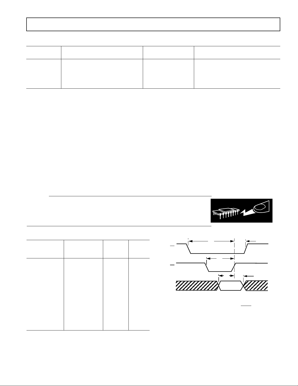
TIMING CHARACTERISTICS
CS
WR
DATA
5V
0V
5V
0V
5V
0V
NOTES
1. ALL INPUT SIGNAL RISE AND FALL TIMES MEASURED FROM
10% TO 90% OF +5V. t
R
= tF = 20ns.
2. TIMING MEASUREMENT REFERENCE LEVEL IS
V
IH
+ V
IL
2
t
CS
t
CH
t
WR
t
DStDH
WARNING!
ESD SENSITIVE DEVICE
1
(VDD = +15 V, ⴞ 5%. VSS = –15 V, ⴞ 5%. V
= +10 V. AGND = DGND = O V.)
REF
AD7845
Limit at T
MIN
to T
MAX
Parameter (All Versions) Units Test Conditions/Comments
t
CS
t
CH
t
WR
t
DS
t
DH
NOTES
1
Guaranteed by design and characterization, not production tested.
Specifications subject to change without notice.
ABSOLUTE MAXIMUM RATINGS
(T
= +25°C unless otherwise stated)
A
VDD to DGND . . . . . . . . . . . . . . . . . . . . . . . . –0.3 V to +17 V
to DGND . . . . . . . . . . . . . . . . . . . . . . . .+0.3 V to –17 V
V
SS
to AGND . . . . . . . . . . . . . . . . VDD + 0.3 V, VSS – 0.3 V
V
REF
to AGND . . . . . . . . . . . . . . . . VDD + 0.3 V, VSS – 0.3 V
V
RFB
to AGND . . . . . . . . . . . . . . . . .VDD + 0.3 V, VSS – 0.3 V
V
RA
to AGND . . . . . . . . . . . . . . . . .VDD + 0.3 V, VSS – 0.3 V
V
RB
to AGND . . . . . . . . . . . . . . . . . VDD + 0.3 V, VSS – 0.3 V
V
RC
to AGND2 . . . . . . . . . . . . . . . VDD + 0.3 V, VSS – 0.3 V
V
OUT
AGND to DGND . . . . . . . . . . . . . . . . . . . . . . . . –0.3 V, V
Digital Input Voltage to DGND . . . . . –0.3 V to VDD + 0.3 V
Power Dissipation (Any Package)
To +75°C . . . . . . . . . . . . . . . . . . . . . . . . . . . . . . 650 mW
30 ns min Chip Select to Write Setup Time
0 ns min Chip Select to Write Hold Time
30 ns min Write Pulsewidth
80 ns min Data Setup Time
0 ns min Data Hold Time
1
Operating Temperature Range
Commercial (J, K Versions) . . . . . . . . . . . . . 0°C to +70°C
Industrial (A, B Versions) . . . . . . . . . . . . –40°C to +85°C
Extended (S, T Versions) . . . . . . . . . . . . –55°C to +125°C
Storage Temperature Range . . . . . . . . . . . –65°C to +150°C
Lead Temperature (Soldering, 10 sec) . . . . . . . . . . . +300°C
NOTES
1
Stresses above those listed under Absolute Maximum Ratings may cause
permanent damage to the device. This is a stress rating only; functional
operation of the device at these or any other conditions above those indicated in
DD
the operational sections of this specification is not implied. Exposure to absolute
maximum rating conditions for extended periods of time may affect device
reliability. Only one Absolute Maximum Rating may be applied at any one time.
2
V
may be shorted to AGND provided that the power dissipation of the
OUT
package is not exceeded.
Derates above +75°C . . . . . . . . . . . . . . . . . . . . . 10 mW/°C
CAUTION
ESD (electrostatic discharge) sensitive device. Electrostatic charges as high as 4000 V readily
accumulate on the human body and test equipment and can discharge without detection.
Although the AD7845 features proprietary ESD protection circuitry, permanent damage may
occur on devices subjected to high energy electrostatic discharges. Therefore, proper ESD
precautions are recommended to avoid performance degradation or loss of functionality.
ORDERING GUIDE
Temperature Accuracy Package
Range @ +25ⴗC Option
Model
2
AD7845JN 0°C to +70°C ±1 LSB N-24
AD7845KN 0°C to +70°C ±1/2 LSB N-24
AD7845JP 0°C to +70°C ±1 LSB P-28A
AD7845KP 0°C to +70°C ±1/2 LSB P-28A
AD7845JR 0°C to +70°C ±1 LSB R-24
AD7845KR 0°C to +70°C ±1/2 LSB R-24
AD7845AQ –40°C to +85°C ±1 LSB Q-24
AD7845BQ –40°C to +85°C ±1/2 LSB Q-24
AD7845AR –40°C to +85°C ±1 LSB R-24
AD7845BR –40°C to +85°C ±1/2 LSB R-24
AD7845SQ/883B –55°C to +125°C ±1 LSB Q-24
AD7845TQ/883B –55°C to +125°C ±1/2 LSB Q-24
AD7845SE/883B –55°C to +125°C ±1 LSB E-28A
NOTES
1
Analog Devices reserves the right to ship either ceramic (D-24A) or cerdip
(Q-24) hermetic packages.
2
To order MIL-STD-883, Class B processed parts, add /883B to part number.
3
E = Leadless Ceramic Chip Carrier; N = Plastic DIP; P = Plastic Leaded Chip
Carrier; Q = Cerdip; R = SOIC.
REV. B –3–
1
Relative
3
Figure 1. AD7845 Timing Diagram
Page 4
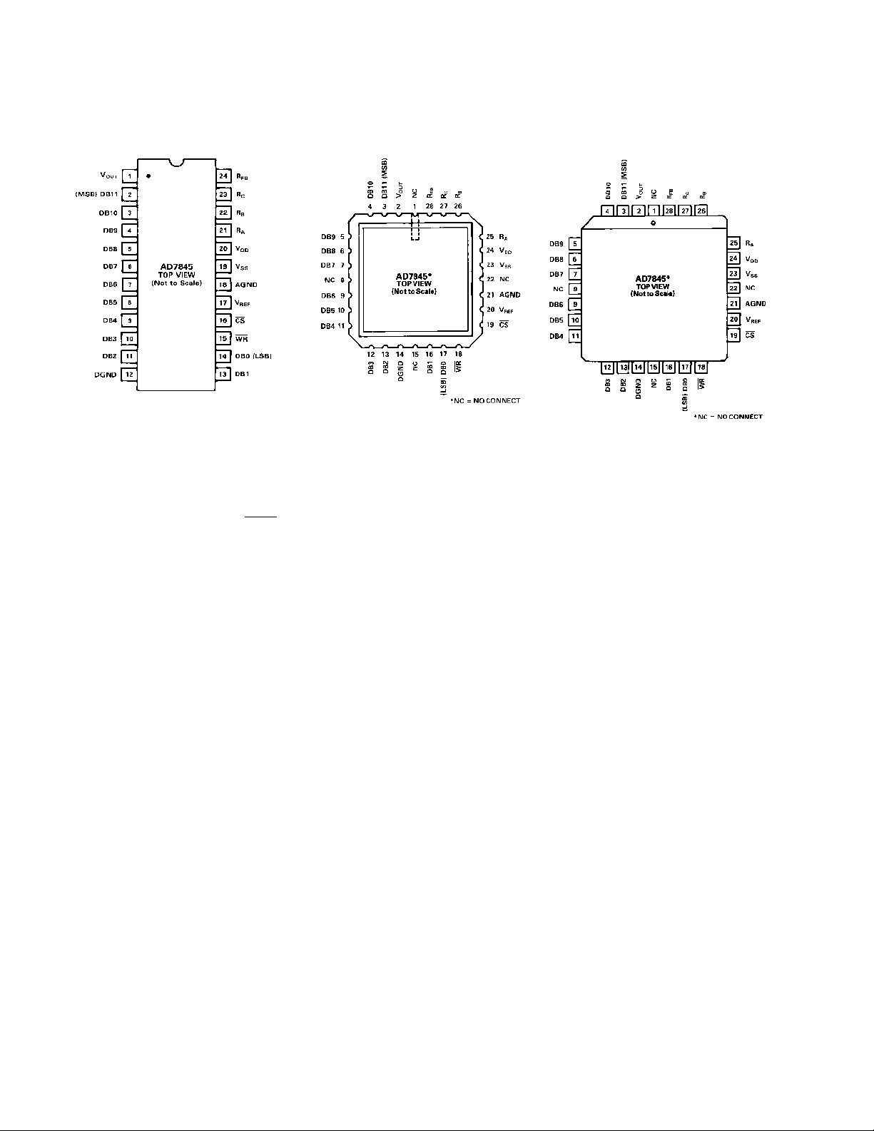
AD7845
PIN CONFIGURATIONS
DIP, SOIC
LCC
TERMINOLOGY
LEAST SIGNIFICANT BIT
This is the analog weighting of 1 bit of the digital word in a
V
REF
DAC. For the AD7845, 1 LSB =
RELATIVE ACCURACY
.
12
2
Relative accuracy or endpoint nonlinearity is a measure of the
maximum deviation from a straight line passing through the
endpoints of the DAC transfer function. It is measured after
adjusting for both endpoints (i.e., offset and gain error are adjusted out) and is normally expressed in least significant bits or
as a percentage of full-scale range.
DIFFERENTIAL NONLINEARITY
Differential nonlinearity is the difference between the measured
change and the ideal 1 LSB change between any two adjacent
codes. A specified differential nonlinearity of +1 LSB max over
the operating temperature range ensures monotonicity.
GAIN ERROR
Gain error is a measure of the output error between an ideal
DAC and the actual device output with all 1s loaded after offset
error has been adjusted out. Gain error is adjustable to zero
with an external potentiometer. See Figure 13.
ZERO CODE OFFSET ERROR
This is the error present at the device output with all 0s loaded
in the DAC. It is due to the op amp input offset voltage and
bias current and the DAC leakage current.
TOTAL HARMONIC DISTORTION
This is the ratio of the root-mean-square (rms) sum of the harmonics to the fundamental, expressed in dBs.
OUTPUT NOISE
This is the noise due to the white noise of the DAC and the
input noise of the amplifier.
PLCC
DIGITAL-TO-ANALOG GLITCH IMPULSE
This is the amount of charge injected from the digital inputs to
the analog output when the inputs change state. This is normally specified as the area of the glitch in either pA-secs or
nV-secs depending upon whether the glitch is measured as a
current or voltage. The measurement takes place with V
REF
=
AGND.
DIGITAL FEEDTHROUGH
When the DAC is not selected (i.e., CS is high) high frequency
logic activity on the device digital inputs is capacitively coupled
through the device to show up as noise on the V
pin. This
OUT
noise is digital feedthrough.
MULTIPLYING FEEDTHROUGH ERROR
This is ac error due to capacitive feedthrough from the V
terminal to V
OPEN-LOOP GAIN
when the DAC is loaded with all 0s.
OUT
REF
Open-loop gain is defined as the ratio of a change of output
voltage to the voltage applied at the V
pin with all 1s loaded
REF
in the DAC. It is specified at dc.
UNITY GAIN SMALL SIGNAL BANDWIDTH
This is the frequency at which the magnitude of the small signal
voltage gain of the output amplifier is 3 dB below unity. The
device is operated as a closed-loop unity gain inverter (i.e.,
DAC is loaded with all 1s).
OUTPUT RESISTANCE
This is the effective output source resistance.
FULL POWER BANDWIDTH
Full power bandwidth is specified as the maximum frequency, at
unity closed-loop gain, for which a sinusoidal input signal will
produce full output at rated load without exceeding a distortion
level of 3%.
–4–
REV. B
Page 5

Typical Performance Characteristics–AD7845
TIME – s
OUTPUT – mV
80
10
–20
0
220
4 6 8 1012141618
70
20
0
–10
40
30
60
50
Figure 2. Frequency Response, G = –1
Figure 5. THD vs. Frequency
Figure 3. Output Voltage Swing vs.
Resistive Load
Figure 6. Typical AD7845 Linearity
vs. Power Supply
Figure 4. Noise Spectral Density
Figure 7. Multiplying Feedthrough
Error vs. Frequency
Figure 8. Unity Gain Inverter Pulse
Response (Large Signal)
REV. B
Figure 9. Unity Gain Inverter Pulse
Response (Small Signal)
–5–
Figure 10. Digital-to-Analog Glitch
Impulse (All 1s to All 0s Transition)
Page 6

AD7845
RRR
2R
2R
2R
2R 2R
BA S9
2R
C
V
REF
S8 S0
SHOWN FOR ALL 1s ON DAC
2R
I
OUT
AGND
PIN FUNCTION DESCRIPTION (DIP)
Pin Mnemonic Description
1V
OUT
2-11 DB11–DB2 Data Bit 11 (MSB) to Data Bit 2
12 DGND Digital Ground. The metal lid on the ceramic package is connected to this pin
13-14 DB1–DB0 Data Bit 1 to Data Bit 0 (LSB)
15 WR Write Input. Active low
16 CS Chip Select Input. Active low
17 V
REF
18 AGND Analog Ground. This is the reference point for external analog circuitry
19 V
20 V
21 R
22 R
23 R
24 R
SS
DD
A
B
C
FB
Voltage Output Terminal
Reference Input Voltage which can be an ac or dc signal
Negative power supply for the output amplifier (nominal –12 V to +15 V)
Positive power supply (nominal +12 V to +15 V)
Application resistor. RA = 4 R
Application resistor. RB = 2 R
Application resistor. RC = 2 R
Feedback resistor in the DAC. For normal operation this is connected to V
FB
FB
FB
OUT
CIRCUIT INFORMATION
Digital Section
Figure 11 is a simplified circuit diagram of the AD7845 input
control logic. When CS and WR are both low, the DAC latch is
loaded with the data on the data inputs. All the digital inputs
are TTL, HCMOS and +5 V CMOS compatible, facilitating
easy microprocessor interfacing. All digital inputs incorporate
standard protection circuitry.
Figure 11. AD7845 Input Control Logic
D/A Section
Figure 12 shows a simplified circuit diagram for the AD7845
D/A section and output amplifier.
A segmented scheme is used whereby the 2 MSBs of the 12-bit
data word are decoded to drive the three switches A-C. The
remaining 10 bits drive the switches (S0–S9) in a standard R-2R
ladder configuration.
Each of the switches A–C steers 1/4 of the total reference current with the remaining 1/4 passing through the R-2R section.
An output amplifier and feedback resistor perform the currentto-voltage conversion giving
V
= – D × V
OUT
REF
where D is the fractional representation of the digital word. (D
can be set from 0 to 4095/4096.)
The amplifier can maintain ±10 V across a 2 kΩ load. It is inter-
nally compensated and settles to 0.01% FSR (1/2 LSB) in less
than 5 µs. The input offset voltage is laser trimmed at wafer
level. The amplifier slew rate is typically 11 V/µs, and the unity
gain small signal bandwidth is 600 kHz. There are three extra
on-chip resistors (R
, RB, RC) connected to the amplifier invert-
A
ing terminal. These are useful in a number of applications including offset adjustment and gain ranging.
Figure 12. Simplified Circuit Diagram for the AD7845 D/A
Section
–6–
REV. B
Page 7

AD7845
UNIPOLAR BINARY OPERATION
Figure 13 shows the AD7845 connected for unipolar binary
operation. When V
is an ac signal, the circuit performs
IN
2-quadrant multiplication. The code table for Figure 13 is given
in Table I.
Figure 13. Unipolar Binary Operation
Table I. Unipolar Binary Code Table for AD7845
BIPOLAR OPERATION
(4-QUADRANT MULTIPLICATION)
The recommended circuit for bipolar operation is shown in
Figure 14. Offset binary coding is used.
The offset specification of this circuit is determined by the
matching of internal resistors R
and RC and by the zero code
B
offset error of the device. Gain error may be adjusted by varying
the ratio of R1 and R2.
To use this circuit without trimming and keep within the gain
error specifications, resistors R1 and R2 should be ratio
matched to 0.01%.
The code table for Figure 14 is given in Table II.
Binary Number In
DAC Register Analog Output, V
MSB LSB
1111 1111 1111 –V
1000 0000 0000 –VIN
0000 0000 0001 –VIN
4095
IN
4096
2048
4096
1
4096
OUT
= –1/2 V
IN
0000 0000 0000 0 V
OFFSET AND GAIN ADJUSTMENT FOR FIGURE 13
Zero Offset Adjustment
1. Load DAC with all 0s.
2. Trim R3 until V
Gain Adjustment
OUT
= 0 V.
1. Load DAC with all 1s.
4095
2. Trim R1 so that V
OUT
= –VIN
4096
.
In fixed reference applications, full scale can also be adjusted by
omitting R1 and R2 and trimming the reference voltage magnitude. For high temperature applications, resistors and potentiometers should have a low temperature coefficient.
Figure 14. Bipolar Offset Binary Operation
Table II. Bipolar Code Table for Offset Binary Circuit of
Figure 14
Binary Number In
DAC Register Analog Output, V
MSB LSB
1111 1111 1111 +V
1000 0000 0001 +VIN
2047
2048
1
2048
IN
1000 0000 0000 0 V
0111 1111 1111 –V
0000 0000 0000 –VIN
1
2048
2048
2048
= –V
IN
OUT
IN
REV. B –7–
Page 8

AD7845
1
R1
D ×|V
IN
|
R
DAC
1 +
R1
R
DAC
APPLI
CATION
PROGRAMMABLE GAIN AMPLIFIER (PGA)
The AD7845 performs a PGA function when connected as in
Figure 15. In this configuration, the R-2R ladder is connected
in the amplifier feedback loop. R
tor. As the code decreases, the R-2R ladder resistance increases
and so the gain increases.
S CIRCUITS
is the amplifier input resis-
FB
PROGRAMMABLE CURRENT SOURCES
The AD7845 is ideal for designing programmable current
sources using a minimum of external components. Figures 16
and 17 are examples. The circuit of Figure 16 drives a programmable current I
into a load referenced to a negative supply.
L
Figure 17 shows the circuit for sinking a programmable current,
. The same set of circuit equations apply for both diagrams.
I
L
V
OUT
= –VIN ×
= –VIN ×
R
DAC
D
R
DAC
D
×
1
×
1
R
DAC
D = 0 to
,
R
FB
–V
IN
=
D
, since RFB = R
4095
4096
DAC
Figure 15. AD7845 Connected as PGA
As the programmed gain increases, the error and noise also
increase. For this reason, the maximum gain should be limited
to 256. Table III shows gain versus code.
Note that instead of using R
as the input resistor, it is also
FB
possible to use combinations of the other application resistors,
, RB and RC. For instance, if RB is used instead of RFB, the
R
A
gain range for the same codes of Table II now goes from l/2
to 128.
= I3 = I2 + I
I
L
D ×|V
I1 =
I2 =
D ×|V
IL =
D ×|V
=
Note that by making R1 much smaller than R
becomes insensitive to both the absolute value of R
R
DAC
R1
R1
1
|
IN
,
D ×|V
R
DAC
|
IN
+
|
IN
×
D = 0 to
|
IN
RFB =
4095
4096
D ×|V
R1
|
IN
, since RFB = R
, the circuit
DAC
DAC
DAC
and its
temperature variations. Now, the only resistor determining load
current I
is the sense resistor R1.
L
If R1 = 100 Ω, then the programming range is 0 mA to 100 mA,
and the resolution is 0.024 mA.
Table III. Gain and Error vs. Input Code for Figure 15
Digital Inputs Gain Error (%)
1111 1111 1111 4096/4095 ≈ 10.04
1000 0000 0000 2 0.07
0100 0000 0000 4 0.13
0010 0000 0000 8 0.26
0001 0000 0000 16 0.51
0000 1000 0000 32 1.02
0000 0100 0000 64 2.0
0000 0010 0000 128 4.0
0000 0001 0000 256 8.0
–8–
Figure 16. Programmable Current Source
REV. B
Page 9

AD7845
Figure 17. Programmable Current Sink
4–20 mA CURRENT LOOP
The AD7845 provides an excellent way of making a 4-20 mA
current loop circuit. This is basically a variation of the circuits
in Figures 16 and 17 and is shown in Figure 18. The application
resistor R
I
(Value 4R) produces the effective 4 mA offset.
A
= I3 = I2 + I
L
1
Since I2 > I1,
I
I
L
L
= –
=
V
156
2.5
4
X
=
+D ×2.5
2.5
× RFB+
4R
and since R
×
1000
156
2.5
R
DAC
DAC=RFB
mA
×D × R
=R
FB
1
×
156
= [4 + (16 × D)]mA, where D goes from 0 to 1 with
Digital Code
When D = 0 (Code of all 0s):
I
= 4 mA
L
When D = 1 (Code of all 1s):
= 20 mA
I
L
The above circuit succeeds in significantly reducing the circuit
component count. Both the on-chip output amplifier and the
application resistor R
contribute to this.
A
Figure 18. 4–20 mA Current Loop
APPLICATION HINTS
General Ground Management: AC or transient voltages
between AGND and DGND can cause noise injection into the
analog output. The simplest method of ensuring that voltages at
AGND and DGND are equal is to tie AGND and DGND
together at the AD7845. In more complex systems where the
AGND and DGND intertie is on the backplane, it is recommended that two diodes be connected in inverse parallel between the AD7845 AGND and DGND pins (IN914 or
equivalent).
Digital Glitches: When a new digital word is written into the
DAC, it results in a change of voltage applied to some of the
DAC switch gates. This voltage change is coupled across the
switch stray capacitance and appears as an impulse on the current output bus of the DAC. In the AD7845, impulses on this
bus are converted to a voltage by R
and the output amplifier.
FB
The output voltage glitch energy is specified as the area of the
resulting spike in nV-seconds. It is measured with V
REF
connected to analog ground and for a zero to full-scale input code
transition. Since microprocessor based systems generally have
noisy grounds which couple into the power supplies, the
AD7845 V
and VSS terminals should be decoupled to signal
DD
ground.
Temperature Coefficients: The gain temperature coefficient
of the AD7845 has a maximum value of 5 ppm/°C. This corresponds to worst case gain shift of 2 LSBs over a 100°C tem-
perature range. When trim resistors R1 and R2 in Figure 13
are used to adjust full-scale range, the temperature coefficient
of R1 and R2 must be taken into account. The offset tempera-
ture coefficient is 5 ppm of FSR/°C maximum. This corresponds to a worst case offset shift of 2 LSBs over a 100°C
temperature range.
The reader is referred to Analog Devices Application Note
“Gain Error and Gain Temperature Coefficient of CMOS Multiplying DACs,” Publication Number E630C-5-3/86.
REV. B –9–
Page 10

AD7845
MICROPROCESSOR INTERFACING
16-BIT MICROPROCESSOR SYSTEMS
Figures 19, 20 and 21 show how the AD7845 interfaces to
three popular 16-bit microprocessor systems. These are the
MC68000, 8086 and the TM32010. The AD7845 is treated as
a memory-mapped peripheral to the processors. In each case, a
write instruction loads the AD7845 with the appropriate data.
The particular instructions used are as follows:
MC68000: MOVE
8086: MOV
TMS32010: OUT
8-BIT MICROPROCESSOR SYSTEMS
Figure 22 shows an interface circuit for the AD7845 to the
8085A 8-bit microprocessor. The software routine to load data
to the device is given in Table IV. Note that the transfer of the
12 bits of data requires two write operations. The first of these
loads the 4 MSBs into the 7475 latch. The second write operation loads the 8 LSBs plus the 4 MSBs (which are held by the
latch) into the DAC.
Figure 22. 8085A Interface
Figure 19. AD7845 to MC68000 Interface
Figure 20. AD7845 to 8086 Interface
Table IV. Subroutine Listing for Figure 22
2000 LOAD DAC: LXI H,#3000 The H,L register pair
are loaded with latch
address 3000.
MVI A,#“MS” Load the 4 MSBs of
data into accumulator.
MOV M,A Transfer data from
accumulator to latch.
INR L Increment H,L pair to
AD7845 address.
MVI A,#“LS” Load the 8 LSBs of
data into accumulator.
MOV M,A Transfer data from
accumulator to DAC.
RET End of routine.
Figure 21. TMS32010
–10–
REV. B
Page 11

AD7845
Figure 23 and 24 are the interface circuits for the Z80 and
MC6809 microprocessors. Again, these use the same basic
format as the 8085A interface.
Figure 23. AD7845 to Z80 Interface
DIGITAL FEEDTHROUGH
In the preceding interface configurations, most digital inputs to
the AD7845 are directly connected to the microprocessor bus.
Even when the device is not selected, these inputs will be constantly changing. The high frequency logic activity on the bus
can feed through the DAC package capacitance to show up as
noise on the analog output. To minimize this digital feedthrough
isolate the DAC from the noise source. Figure 25 shows an
interface circuit which uses this technique. All data inputs are
latched from the busy by the CS signal. One may also use other
means, such as peripheral interface devices, to reduce the digital
feedthrough.
Figure 25. AD7845 Interface Circuit Using Latches to
Minimize Digital Feedthrough
Figure 24. MC6809 Interface
REV. B –11–
Page 12

AD7845
0.0125 (0.32)
0.0091 (0.23)
88
08
0.0291 (0.74)
0.0098 (0.25)
3 458
0.0500 (1.27)
0.0157 (0.40)
SEATING
PLANE
0.0118 (0.30)
0.0040 (0.10)
0.0192 (0.49)
0.0138 (0.35)
0.1043 (2.65)
0.0926 (2.35)
0.0500
(1.27)
BSC
24 13
12
1
0.4193 (10.65)
0.3937 (10.00)
0.2992 (7.60)
0.2914 (7.40)
PIN 1
0.6141 (15.60)
0.5985 (15.20)
OUTLINE DIMENSIONS
Dimensions shown in inches and (mm).
24-Lead Plastic DIP
(N-24)
24-Lead Cerdip
(Q-24)
28-Terminal Leadless Ceramic Chip Carrier
(E-28A)
C1189b–1–9/99
28-Terminal Plastic Leaded Chip Carrier
(P-28A)
24-Lead Ceramic DIP
(D-24A)
–12–
24-Lead SOIC
(R-24)
PRINTED IN U.S.A.
REV. B
 Loading...