

Page 1
3 V/5 V, 1 MSPS, 8-Bit, Serial Interface
BUF
T/H
2.5V
REF
8-BIT
HALF-FLASH
ADC
SERIAL
PORT
CONTROL
LOGIC
V
DD
DETECT
RFS
D
OUT
SCLK
CONVST
GND
V
DD
V
REFIN/VREFOUT
V
IN
COMP
AD7827
a
FEATURES
8-Bit Half-Flash ADC with 420 ns Conversion Time
200 ns Acquisition Time
8-Lead Package
On-Chip Track-and-Hold
On-Chip 2.5 V Reference with 2% Tolerance
Operating Supply Range: 3 V 6 10% and 5 V 6 10%
Specifications @ 3 V and 5 V
DSP/Microcontroller Compatible Serial Interface
Automatic Power-Down at End of Conversion
Input Ranges
0 V to 2 V, V
0 V to 2.5 V, V
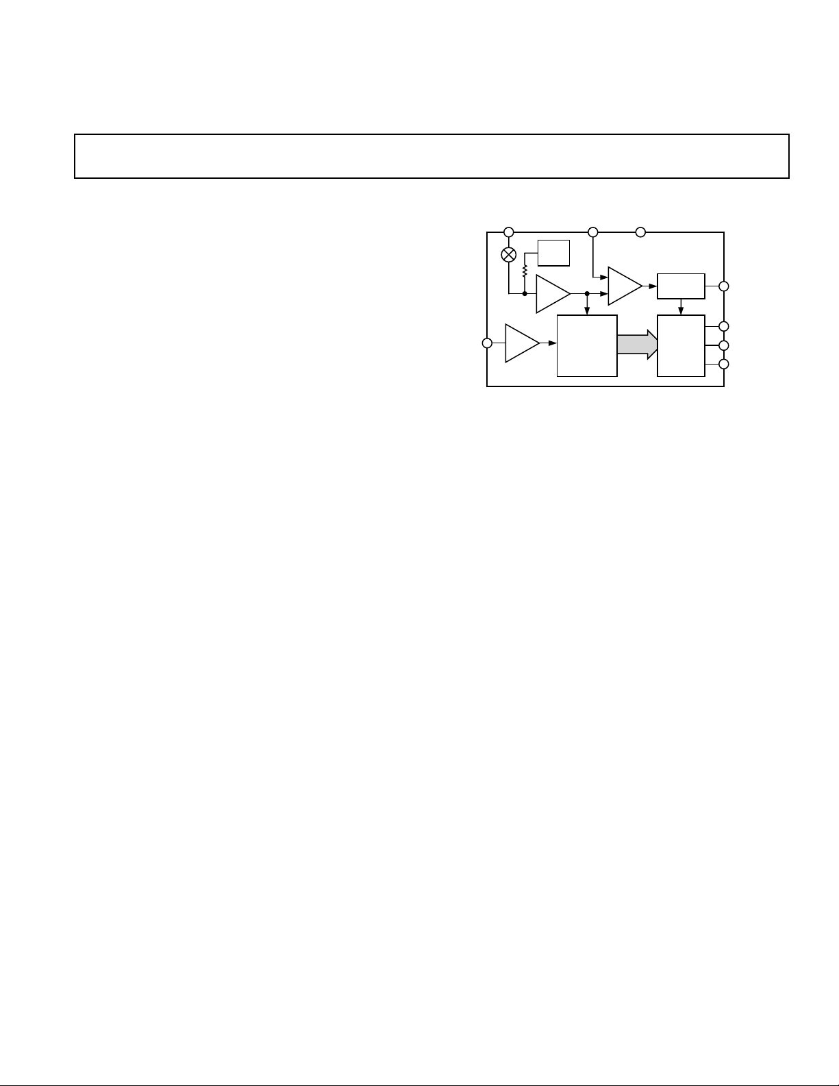
GENERAL DESCRIPTION
The AD7827 is a high speed, single channel, low power, analogto-digital converter with a maximum throughput of 1 MSPS that
operates from a single 3 V or 5 V supply. The AD7827 contains
a track/hold amplifier, an on-chip 2.5 V reference (2% tolerance), a 420 ns 8-bit half-flash ADC and a serial interface. The
serial interface is compatible with the serial interfaces of most
DSPs (Digital Signal Processors). The throughput rate of the
AD7827 is dependent on the clock speed of the DSP serial
interface.
The AD7827 combines the Convert Start and Power Down
signals at one pin, i.e., the CONVST pin. This allows a unique
automatic power-down at the end of a conversion to be implemented. The logic level on the CONVST pin is sampled at the
end of a conversion and, depending on its state, the AD7827
powers down.
The AD7827 has one single-ended analog input with an input
span determined by the supply voltage. With a V
input range of the AD7827 is 0 V to 2 V and with V
5 V, the input range is 0 V to 2.5 V.
The parts are available in a small, 8-lead, 0.3" wide, plastic
dual-in-line package (DIP) and an 8-lead, small outline IC
(SOIC).
= 3 V
DD
DD
= 5 V
of 3 V, the
DD
equal to
DD
Sampling ADC
AD7827
FUNCTIONAL BLOCK DIAGRAM
PRODUCT HIGHLIGHTS
1. Fast Conversion Time
The AD7827 has a conversion time of 420 ns. Faster conversion times maximize the DSP processing time in a real time
system.
2. Built-In Track-and-Hold
The analog input signal is held and a new conversion is initiated on the falling edge of the CONVST signal. The CONVST
signal allows the sampling instant to be exactly controlled.
This feature is a requirement in many DSP applications.
3. Automatic Power-Down
The CONVST signal is sampled approximately 100 ns after
the end of conversion and depending on its state the AD7827
is powered down.
4. An easy to use, fast serial interface allows direct interfacing to
most popular DSPs with no external circuitry.
REV. 0
Information furnished by Analog Devices is believed to be accurate and
reliable. However, no responsibility is assumed by Analog Devices for its
use, nor for any infringements of patents or other rights of third parties
which may result from its use. No license is granted by implication or
otherwise under any patent or patent rights of Analog Devices.
One Technology Way, P.O. Box 9106, Norwood, MA 02062-9106, U.S.A.
Tel: 781/329-4700 World Wide Web Site: http://www.analog.com
Fax: 781/326-8703 © Analog Devices, Inc., 1998
Page 2

AD7827–SPECIFICA TIONS
(VDD = +3 V 6 10%, VDD = +5 V 6 10%, GND = 0 V, V
REFIN/REFOUT
specifications –408C to +1058C unless otherwise noted.)
= 2.5 V. All
Parameter Version B Units Test Conditions/Comments
DYNAMIC PERFORMANCE f
Signal-to-(Noise + Distortion) Ratio
Total Harmonic Distortion
Peak Harmonic or Spurious Noise
Intermodulation Distortion
1
1
1
1
48 dB min
–55 dB max
–55 dB max
= 30 kHz; f
IN
fa = 29.1 kHz; fb = 29.9 kHz
SAMPLE
= 1 MHz
2nd Order Terms –65 dB typ
3rd Order Terms –65 dB typ
DC ACCURACY
Resolution 8 Bits
Integral Nonlinearity (INL)
Differential Nonlinearity (DNL)
Offset Error
Gain Error
1
1
1
1
±0.5 LSB max
±0.5 LSB max
±1.5 LSB max
±2 LSB max
Minimum Resolution for Which
No Missing Codes are Guaranteed 8 Bits
ANALOG INPUT
2
Input Voltage Range 0 V min VDD = 5 V
2.5 V max
0 V min V
DD
= 3 V
2 V max
Input Leakage Current ±1 µA max
Input Capacitance 10 pF max
REFERENCE INPUT
V
REFIN/REFOUT
Input Voltage Range 2.55 V max
2.45 V min
Input Current ±1 µA typ
±50 µA max
LOGIC INPUTS
CONVST, SCLK
V
Input High Voltage 2.4 V min VDD = 5 V ± 10%
INH,
V
Input Low Voltage 0.8 V max VDD = 5 V ± 10%
INL,
V
Input High Voltage 2.0 V min VDD = 3 V ± 10%
INH,
V
Input Low Voltage 0.4 V max VDD = 3 V ± 10%
INL,
Input Current, I
INH
±1 µA max Typically 10 nA, VIN = 0 V or V
Input Capacitance 10 pF max
LOGIC OUTPUTS
D
, RFS
OUT
V
Output High Voltage I
OH,
4 V max V
2.4 V min V
V
Output Low Voltage I
OL,
0.4 V max V
0.2 V min V
High Impedance Leakage Current ±1 µA max
High Impedance Capacitance 15 pF max
CONVERSION RATE
Conversion Time 420 ns max
Track/Hold Acquisition Time 200 ns max
= 200 µA
SOURCE
= 5 V ± 10%
DD
= 3 V ± 10%
DD
= 200 µA
SINK
= 5 V ± 10%
DD
= 3 V ± 10%
DD
DD
–2–
REV. 0
Page 3
AD7827
Parameter Version B Units Test Conditions/Comments
POWER SUPPLY
V
DD
I
DD
Normal Operation 10 mA max 8 mA Typically
Power-Down 1 µA max Logic Inputs = 0 V or V
Power Dissipation VDD = 3 V
Normal Operation 30 mW max Typically 24 mW
Power-Down
200 kSPS 9.58 mW max
1 MSPS 47.88 mW max
NOTES
1
See Terminology section of this data sheet.
2
Refer to the Analog Input section for an explanation of the Analog Input(s).
Specifications subject to change without notice.
TIMING CHARACTERISTICS
Parameter 5 V 6 10% 3 V 6 10% Units Conditions/Comments
t
CONVERT
t
1
t
2
3
t
3
t
4
3
t
5
3
t
6
t
7
t
8
4
t
9
t
10
t
11
t
POWER-UP
t
POWER-UP
NOTES
1
Sample tested to ensure compliance.
2
See Figures 13, 14 and 15.
3
Measured with the load circuit of Figure 1 and defined as the time required for an output to cross 0.8 V or 2.4 V with VDD = 5 V ± 10% and time required for an
output to cross 0.4 V or 2.0 V with VDD = 3 V ± 10%.
4
Derived from the measured time taken by the data outputs to change 0.5 V when loaded with the circuit of Figure 1. The measured number is then extrapolated back
to remove the effects of charging or discharging the 50 pF capacitor. This means that the time, t9, quoted in the timing characteristics is the true bus relinquish time of
the part and as such is independent of external bus loading capacitances.
Specifications subject to change without notice.
420 420 ns max Conversion Time.
20 20 ns min Minimum CONVST Pulsewidth.
t
CONVERT+t3
t
CONVERT+t3+t7+t8tCONVERT+t3+t7+t8
t
CONVERT+t3
14 18 ns max Rising edge of SCLK to falling edge of RFS.
14 18 ns max Rising edge of SCLK to rising edge of RFS.
20 20 ns max Rising edge of SCLK to high impedance disabled.
14 18 ns max Rising edge of SCLK to D
25 25 ns min Minimum high SCLK pulse duration.
25 25 ns min Minimum low SCLK pulse duration.
20 20 ns min Bus relinquish time after SCLK falling edge.
35 35 ns max
20 20 ns max Maximum delay from falling edge CONVST to rising edge RFS if
30 30 ns min Minimum time between end of serial read and next falling edge of
11µs max Power-up time from rising edge of CONVST using external 2.5 V
25 25 µs max Power-up time from rising edge of CONVST using on-chip reference.
4.5 V min 5 V ± 10% For Specified Performance
5.5 V max
2.7 V min 3 V ± 10% For Specified Performance
3.3 V max
1, 2
(V
REFIN/REFOUT
= 2.5 V, all specifications –408C to +1058C, unless otherwise noted)
ns min Falling edge of CONVST to falling edge of RFS.
ns max
valid delay.
OUT
RFS reset by CONVST.
CONVST.
reference.
200mA
I
OL
DD
TO
OUTPUT
PIN
50pF
C
L
200mA
+2.1V
I
OH
Figure 1. Load Circuit for Digital Output Timing Specifications
–3–REV. 0
Page 4
AD7827
WARNING!
ESD SENSITIVE DEVICE
TOP VIEW
(Not to Scale)
8
7
6
5
1
2
3
4
CONVST
V
IN
RFS
V
DD
SCLK
D
OUT
V
REF
GND
AD7827
ABSOLUTE MAXIMUM RATINGS*
V
to GND . . . . . . . . . . . . . . . . . . . . . . . . . . –0.3 V to +7 V
DD
Digital Input Voltage to GND
(CONVST, SCLK) . . . . . . . . . . . . . . –0.3 V, V
+ 0.3 V
DD
Digital Output Voltage to GND
(D
, RFS) . . . . . . . . . . . . . . . . . . . –0.3 V, VDD + 0.3 V
OUT
V
to GND . . . . . . . . . . . . . . . . . . . . . . –0.3 V, V
REF
Analog Input Voltage to AGND . . . . . . –0.3 V, V
+ 0.3 V
DD
+ 0.3 V
DD
Operating Temperature Range
Industrial (B Version) . . . . . . . . . . . . . . . –40°C to +105°C
Storage Temperature Range . . . . . . . . . . . . –65°C to +150°C
Lead Temperature (Soldering, 10 sec) . . . . . . . . . . . +300°C
Plastic DIP Package, Power Dissipation . . . . . . . . . . 450 mW
θ
Thermal Impedance . . . . . . . . . . . . . . . . . . . +105°C/W
JA
Lead Temperature, (Soldering 10 sec) . . . . . . . . . . +260°C
SOIC Package, Power Dissipation . . . . . . . . . . . . . . . 450 mW
θ
Thermal Impedance . . . . . . . . . . . . . . . . . . . . +75°C/W
JA
Lead Temperature, Soldering
Vapor Phase (60 sec) . . . . . . . . . . . . . . . . . . . . . +215°C
Infrared (15 sec) . . . . . . . . . . . . . . . . . . . . . . . . . +220°C
ESD . . . . . . . . . . . . . . . . . . . . . . . . . . . . . . . . . . . . . . . 2.0 kV
*Stresses above those listed under Absolute Maximum Ratings may cause perma-
nent damage to the device. This is a stress rating only; functional operation of the
device at these or any other conditions above those listed in the operational
sections of this specification is not implied. Exposure to absolute maximum rating
conditions for extended periods may affect device reliability.
ORDERING GUIDE
Linearity
Error Package Package
Model (LSB) Description Option
AD7827BN ±0.5 LSB Plastic DIP N-8
AD7827BR ±0.5 LSB Small Outline IC SO-8
PIN FUNCTION DESCRIPTIONS
Pin No. Mnemonic Description
1 CONVST Convert Start. Puts the track-and-
hold into hold mode and initiates a
conversion.
The state of this pin at the end of
conversion also determines whether
or not the part is powered down.
2V
IN
Analog Input is applied here.
3 RFS Receive Frame Sync. This is an
output. When this signal goes logic
high at the end of a conversion, the
DSP starts latching in data on the
next cycle of SCLK.
4 GND Ground reference for analog and
digital circuitry.
5V
6D
REF
OUT
Reference Input.
Serial Data is shifted out on this pin.
Data is clocked out by the rising
edges of SCLK.
7 SCLK Serial Clock. An external serial clock
is applied here. The clock must be
continuous so the RFS (frame SYNC)
can be synchronized to the clock for
high speed data transfers. (See
Microprocessor Interfacing section.)
8VDDPositive Supply Voltage 3 V/5 V ± 10%.
PIN CONFIGURATION
CAUTION
ESD (electrostatic discharge) sensitive device. Electrostatic charges as high as 4000 V readily
accumulate on the human body and test equipment and can discharge without detection.
Although the AD7827 features proprietary ESD protection circuitry, permanent damage may
occur on devices subjected to high energy electrostatic discharges. Therefore, proper ESD
precautions are recommended to avoid performance degradation or loss of functionality.
–4–
REV. 0
Page 5

AD7827
TERMINOLOGY
Signal-to-(Noise + Distortion) Ratio
This is the measured ratio of signal-to-(noise + distortion) at
the output of the A/D converter. The signal is the rms amplitude
of the fundamental. Noise is the rms sum of all nonfundamental
signals up to half the sampling frequency (f
/2), excluding dc.
S
The ratio is dependent upon the number of quantization levels in
the digitization process; the more levels, the smaller the quantization noise. The theoretical signal-to-(noise + distortion) ratio for
an ideal N-bit converter with a sine wave input is given by:
Signal-to-(Noise + Distortion) = (6.02N + 1.76) dB
Thus for an 8-bit converter, this is 50 dB.
Total Harmonic Distortion
Total harmonic distortion (THD) is the ratio of the rms sum of
harmonics to the fundamental. For the AD7827 it is defined as:
2
2
2
2
2
+V
5
6
THD (dB)=20 log
+V
+V
V
2
3
+V
4
V
1
where V1 is the rms amplitude of the fundamental and V2, V3, V4,
V
and V6 are the rms amplitudes of the second through the sixth
5
harmonics.
Peak Harmonic or Spurious Noise
Peak harmonic or spurious noise is defined as the ratio of the
rms value of the next largest component in the ADC output
spectrum (up to f
/2 and excluding dc) to the rms value of the
S
fundamental. Normally, the value of this specification is determined by the largest harmonic in the spectrum, but for parts
where the harmonics are buried in the noise floor, it will be a
noise peak.
Intermodulation Distortion
With inputs consisting of sine waves at two frequencies, fa and
fb, any active device with nonlinearities will create distortion
products at sum and difference frequencies of mfa ± nfb where
m, n = 0, 1, 2, 3, etc. Intermodulation terms are those for
which neither m nor n are equal to zero. For example, the second order terms include (fa + fb) and (fa – fb), while the third
order terms include (2fa + fb), (2fa – fb), (fa + 2fb) and (fa – 2fb).
The AD7827 is tested using the CCIF standard where two
input frequencies near the top end of the input bandwidth are
used. In this case, the second and third order terms are of different significance. The second order terms are usually distanced in frequency from the original sine waves while the third
order terms are usually at a frequency close to the input frequencies. As a result, the second and third order terms are
specified separately. The calculation of the intermodulation
distortion is as per the THD specification where it is the ratio
of the rms sum of the individual distortion products to the rms
amplitude of the fundamental expressed in dBs.
Relative Accuracy
Relative accuracy or endpoint nonlinearity is the maximum
deviation from a straight line passing through the endpoints of
the ADC transfer function.
Differential Nonlinearity
This is the difference between the measured and the ideal
1 LSB change between any two adjacent codes in the ADC.
Offset Error
This is the deviation of the 128th code transition (01111111) to
(10000000) from the ideal, i.e., V
(V
= 3 V).
DD
/2 (VDD = 5 V), 0.8 V
REF
REF
/2
Zero Scale Error
This is the deviation of the first code transition (00000000) to
(00000001) from the ideal, i.e., V
5 V ± 10%), or 0.8 V
/2 –1.0 V + 1 LSB (VDD = 3 V ± 10%).
REF
/2 –1.25 V + 1 LSB (VDD =
REF
Full-Scale Error
This is the deviation of the last code transition (11111110) to
(11111111) from the ideal, i.e., V
5 V ± 10%), or V
+ 1.0 V – 1 LSB (VDD = 3 V ± 10%).
MID
+ 1.25 V – 1 LSB (VDD =
MID
Gain Error
This is the deviation of the last code transition (1111...110) to
(1111 . . . 111) from the ideal, i.e., V
– 1 LSB, after the offset
REF
error has been adjusted out.
Track/Hold Acquisition Time
Track/hold acquisition time is the time required for the output
of the track/hold amplifier to reach its final value, within
± 1/2 LSB, after the point at which the track/hold returns to
track mode. This happens approximately 120 ns after the falling
edge of CONVST.
It also applies when there is a step input change on the input
voltage applied to the V
input of the AD7827. It means that
IN
the user must wait for the duration of the track/hold acquisition
time after the end of conversion or after a step input change to
V
before starting another conversion, to ensure that the part
IN
operates to specification.
–5–REV. 0
Page 6

AD7827
CIRCUIT DESCRIPTION
The AD7827 consists of a track-and-hold amplifier followed by
a half-flash analog-to-digital converter. This device uses a halfflash conversion technique where one 4-bit flash ADC is used to
achieve an 8-bit result. The 4-bit flash ADC contains a sampling
capacitor followed by 15 comparators that compare the unknown
input to a reference ladder to get a 4-bit result. This first flash,
i.e., coarse conversion, provides the 4 MSBs. For a full 8-bit
reading to be realized, a second flash, i.e., a fine conversion,
must be performed to provide the 4 LSBs. The 8-bit word is
then placed in the serial shift register.
Figures 2 and 3 below show simplified schematics of the ADC.
When the ADC starts a conversion, the track-and-hold goes into
hold mode and holds the analog input for 120 ns. This is the
acquisition phase as shown in Figure 2 when Switch 2 is in
Position A. At the point when the track-and-hold returns to its
track mode, this signal is sampled by the sampling capacitor as
Switch 2 moves into Position B. The first flash occurs at this
instant and is then followed by the second flash. Typically the
first flash is complete after 100 ns, i.e., at 220 ns, while the end
REFERENCE
R16
SAMPLING
CAPACITOR
T/H
HOLD
A
SW2
B
TIMING AND
CONTROL
LOGIC
V
IN
R15
R14
R13
15
14
D
13
.
.
DECODE LOGIC
.
.
1
R1
OUTPUT REGISTER
OUT
OUTPUT DRIVER
Figure 2. ADC Acquisition Phase
REFERENCE
R16
SAMPLING
CAPACITOR
T/H
HOLD
A
SW2
B
TIMING AND
CONTROL
LOGIC
V
IN
R15
R14
R13
15
14
D
13
.
.
DECODE LOGIC
.
.
1
R1
OUTPUT REGISTER
OUT
OUTPUT DRIVER
of the second flash, and hence the 8-bit conversion result, is
available at 330 ns. As shown in Figure 4 the track-and-hold
returns to track mode after 120 ns, and so starts the next acquisition before the end of the current conversion. Figure 6 shows
the ADC transfer function.
120ns
HOLDHOLD TRACKTRACK
t
10
CONVST
RFS
SCLK
D
OUT
t
1
t
2
t
t
3
12345678
DB7 DB6 DB5 DB4 DB3 DB2 DB1 DB0
7
t
8
t
4
Figure 4. Track-and-Hold Timing
TYPICAL CONNECTION DIAGRAM
Figure 5 shows a typical connection diagram for the AD7827.
The serial interface is implemented using three wires; the RFS is
a logic output and the serial clock is continuous. The Receive
Frame Sync signal (RFS) idles high, the falling edge of CONVST
initiates a conversion and the first rising edge of the serial clock
after the end of conversion causes the RFS signal to go low.
This falling edge of RFS is used to drive the RFS on a microprocessor—see Serial Interface section for more details. V
connected to a voltage source such as the AD780, while V
REF
DD
is
is
connected to a voltage source of 3 V ± 10% or 5 V ± 10%. Due
to the proximity of the CONVST and V
mended to use a 10 nF decoupling capacitor on V
pins, it is recom-
IN
. When V
IN
DD
is first connected the AD7827 powers up in a low current mode,
i.e., power-down. A rising edge on the CONVST pin will cause
the AD7827 to fully power up. For applications where power
consumption is of concern, the automatic power-down at the
end of a conversion should be used to improve power performance. See the Power-Down Options section of this data sheet.
2.5V
V
DDVREF
V
IN
GND
AD780
AD7827
THREE-WIRE
SERIAL INTERFACE
SCLK
D
OUT
RFS
CONVST
mC/mP
SUPPLY
+3V 610% OR
+5V 610%
0V TO 2.5V (V
0V TO 2V (V
10mF
DD
DD
= 5V)
= 3V)
INPUT
0.1mF
Figure 5. Typical Connection Diagram
Figure 3. ADC Conversion Phase
–6–
REV. 0
Page 7

AD7827
ADC TRANSFER FUNCTION
The output coding of the AD7827 is straight binary. The
designed code transitions occur at successive integer LSB
values (i.e., 1 LSB, 2 LSBs, etc.). The LSB size is = V
(V
= 5 V) or the LSB size = (0.8 V
DD
)/256 (VDD = 3 V). The
REF
REF
/256
ideal transfer characteristic for the AD7827 is shown in Figure 6
below.
(VDD = 5V)
DD
/2 – 1V
/256
REF
REF
= 3V) 0.8V
V
REF
0.8V
= 3V)
(V
DD
1LSB = 0.8V
/2
/2
REF
/2+1.25V – 1LSB
/2+1V – 1LSB
REF
REF
/256
11111111
111....110
111....000
10000000
000....111
ADC CODE
000....010
000....001
00000000
(VDD = 5V) V
= 3V) 0.8V
(V
DD
1LSB = V
1LSB (VDD = 5V) V
(V
/2 – 1.25V
REF
REF
Figure 6. Transfer Characteristic
ANALOG INPUT
The AD7827 has a single input channel with an input range of
0 V to 2.5 V or 0 V to 2.0 V, depending on the supply voltage
(V
). This input range is automatically set up by an on-chip
DD
“V
detector” circuit. 5 V operation of the ADC is detected
DD
when V
V
DD
exceeds 4.1 V and 3 V operation is detected when
DD
falls below 3.8 V. This circuit also possesses a degree of
glitch rejection; for example, a glitch from 5.5 V to 2.7 V up to
60 ns wide will not trip the V
Note: Although there is a V
detector.
DD
pin from which a voltage refer-
REF
ence of 2.5 V may be sourced, or to which an external reference
may be applied, this does not provide an option of varying the value
of the voltage reference. As stated in the specifications for the
AD7827, the input voltage range at this pin is 2.5 V ± 2%.
Analog Input Structure
Figure 7 shows an equivalent circuit of the analog input structure of the AD7827. The two diodes, D1 and D2, provide ESD
protection for the analog inputs. Care must be taken to ensure
that the analog input signal never exceeds the supply rails by
more than 200 mV. This will cause these diodes to become
forward biased and start conducting current into the substrate.
The maximum current these diodes can conduct without causing irreversible damage to the part is 20 mA. The capacitor C2
in Figure 7 is typically about 4 pF and can mostly be attributed
to pin capacitance. The resistor R1 is a lumped component
made up of the on resistance of several components including
that of the multiplexer and the track-and-hold. This resistor is
typically about 310 Ω. The capacitor C1 is the track-and-hold
capacitor and has a capacitance of 0.5 pF. Switch 1 is the trackand-hold switch, while Switch 2 is that of the sampling capacitor as shown in Figures 2 and 3.
When in track phase, Switch 1 is closed and Switch 2 is in
Position A. When in hold mode, Switch 1 opens while Switch 2
remains in Position A. The track-and-hold remains in hold
mode for 120 ns—see Circuit Description, after which it returns
to track mode and the ADC enters its conversion phase. At this
point Switch 1 opens and Switch 2 moves to Position B. At the
end of the conversion Switch 2 moves back to Position A.
V
DD
SW1
C1
0.5pF
SW2
A
B
D1
R1
V
IN
C2
4pF
310V
D2
Figure 7. Equivalent Analog Input Circuit
The on-chip track-and-hold can accommodate input frequencies to 10 MHz, making the AD7827 ideal for subsampling
applications. When the AD7827 is converting a 10 MHz input
signal at a sampling rate of 1 MSPS, the effective number of
bits typically remains above seven corresponding to a signal-tonoise ratio of 42 dBs as shown in Figure 8.
50
F
= 1MHz
SAMPLE
48
46
44
SNR – dB
42
40
38
0.2 10134568
INPUT FREQUENCY – MHz
Figure 8. SNR vs. Input Frequency On the AD7827
–7–REV. 0
Page 8

AD7827
POWER-UP TIMES
The AD7827 has a 1 µs power-up time when using an external
reference and a 25 µs power-up time when using the on-chip
reference. When V
is first connected, the AD7827 is in a low
DD
current mode of operation. In order to carry out a conversion
the AD7827 must first be powered up. The AD7827 is powered up by a rising edge on the CONVST pin and a conversion
is initiated on the falling edge of CONVST. Figure 9 shows
how to power up the AD7827 when V
is first connected or
DD
after the ADC has been powered down using the CONVST pin
when using either the on-chip, or an external, reference. When
using an external reference the falling edge of CONVST may
occur before the required power-up time has elapsed; however,
the conversion will not be initiated on the falling edge of
CONVST but rather at the moment when the part has completely powered up, i.e., after 1 µs. If the falling edge of
CONVST occurs after the required power-up time has elapsed,
it is upon this falling edge that a conversion is initiated. When
using the on-chip reference, it is necessary to wait the required
power-up time of approximately 25 µs before initiating a con-
version, i.e., a falling edge on CONVST may not occur before
the required power-up time has elapsed, when V
is first con-
DD
nected or after the AD7827 has been powered down using the
CONVST pin as shown in Figure 9.
EXTERNAL REFERENCE
V
DD
CONVST
t
POWER-UP
1ms
For example, if the AD7827 is operated in a continuous sampling mode, with a throughput rate of 100 kSPS and using an
external reference, the power consumption is calculated as
follows. The power dissipation during normal operation is
30 mW, V
CONVST
DD
t
= 3 V.
POWER-UP
1ms
t
CONVERT
330ns
10ms @ 100kSPS
t
CYCLE
POWER-DOWN
Figure 10. Automatic Power-Down
If the power-up time is 1 µs and the conversion time is 330 ns
(@ 25°C), the AD7827 can be said to dissipate 30 mW for 1.33 µs
(worst case) during each conversion cycle. If the throughput
rate is 100 kSPS, the cycle time is 10 µs and the average power
dissipated during each cycle is (1.33/10) × (30 mW) = 3.99mW.
Figure 11 shows the Power vs. Throughput rate for automatic
full power-down.
100
10
CONVERSION INITIATED HERE
ON-CHIP REFERENCE
V
DD
CONVST
t
POWER-UP
25ms
CONVERSION INITIATED HERE
Figure 9. Power-Up Time
POWER VS. THROUGHPUT
Superior power performance can be achieved by using the
automatic power-down (Mode 2) at the end of a conversion
(see Operating Modes section of this data sheet).
Figure 10 shows how the automatic power-down is implemented
using the CONVST signal to achieve the optimum power performance for the AD7827. The duration of the CONVST pulse
is set to be equal to or less than the power-up time of the devices (see Operating Modes section). As the throughput rate is
reduced, the device remains in its power-down state for longer and
the average power consumption over time drops accordingly.
POWER – mW
1
0.1
0 50050 100 150 200 250 300 350 400 450
THROUGHPUT – kSPS
Figure 11. Power vs. Throughput
0
–10
–20
–30
–40
dB
–50
–60
–70
–80
0 50050
100 150 200 250 300 350 400 450
FREQUENCY – Hz
2048 POINT FFT
SAMPLING
1MSPS
F
IN
Figure 12. AD7827 SNR
= 30kHz
–8–
REV. 0
Page 9

AD7827
OPERATING MODES
The AD7827 has two possible modes of operation depending on
the state of the CONVST pulse at the end of a conversion.
Mode 1 Operation (High Speed Sampling)
When the AD7827 is operated in Mode 1 the device is not
powered down between conversions. This mode of operation
allows high throughput rates to be achieved. Figure 13 shows
how this optimum throughput rate is achieved by bringing
CONVST high before the end of the conversion. When operating in this mode, a new conversion should not be initiated until
30 ns after the end of a read operation. This is to allow the
track/hold to acquire the analog signal to 0.5 LSB accuracy.
t
2
CONVST
t
1
RFS
Mode 2 Operation (Automatic Power-Down)
When the AD7827 is operated in Mode 2 (see Figure 14) it
automatically powers down 530 ns after the falling edge of
CONVST. The CONVST signal is brought low to initiate a
conversion and is left logic low until 530 ns has elapsed after the
falling edge of the CONVST pulse, i.e., before Point A or Point
B in Figure 14, depending on the actual value of t
(see Timing
2
Characteristics). The state of the CONVST signal is sampled at
this point (i.e., 530 ns after CONVST falling edge) and the
AD7827 will power down as long as the CONVST is low. The
ADC is powered up again on the rising edge of the CONVST
signal. The CONVST pulse width does not have to be as long as
the power-up time if an external reference is used (see Power-Up
Times section). Superior power performance can be achieved in
this mode of operation by powering up the AD7827 to only
carry out a conversion. The serial interface of the AD7827 is
still fully operational while the device is powered down.
SCLK
D
OUT
CONVST
RFS
SCLK
D
OUT
t
POWER-UP
CURRENT CONVERSION
RESULT
Figure 13. Mode 1 Operation Timing Diagram
t
2
A
B
CURRENT CONVERSION
RESULT
Figure 14. Mode 2 Operation Timing Diagram
–9–REV. 0
Page 10

AD7827
AD7827 SERIAL INTERFACE
In order to achieve a high throughput rate, the serial port of the
AD7827 has been optimized for high speed serial protocols.
Many high speed serial protocols use a continuous serial clock
to transfer data, e.g., the serial ports of many popular DSPs like
the TMS320C5x, ADSP-21xx and DSP560xx. The serial interface of the AD7827 is optimized for communication with such
devices.
The serial interface of the AD7827 uses a three-wire interface to
communicate with a Master. The serial clock pin (SCLK) is a
logic input and determines the bit transfer rate. The Receive
Frame Synchronization pin (RFS) is a logic output and used to
t
1
CONVST
t
2
RFS
t7t
6
SCLK
D
OUT
t
3
12345678
t
5
DB7 DB6 DB5 DB4 DB3 DB2 DB1 DB0
t
synchronize the data with a continuous serial clock. The data
output pin (D
) is a logic output and serial data is shifted
OUT
out onto this pin on the rising edge of the serial clock. The first
rising edge of the serial clock after the end of a conversion causes
the RFS pin to go logic low. (See Figure 15 below.) The D
OUT
pin
leaves its high impedance state and the first MSB is shifted out
on the first SCLK rising edge after the end of conversion. The
remaining seven data bits are shifted out on subsequent SCLK
rising edges. The D
pin enters its high impedance state again
OUT
on the falling edge of the eighth SCLK after RFS goes low. The
RFS output goes high again on the rising edge of the ninth SCLK.
If the AD7827 does not receive a ninth SCLK, the RFS will be
reset logic high by the next falling edge of CONVST.
t
10
8
t
4
t
11
t
9
Figure 15. Serial Timing
–10–
REV. 0
Page 11

AD7827
MICROPROCESSOR INTERFACING
The Serial Interface on the AD7827 allows the part to be connected directly to a range of many different microprocessors and
microcontrollers. This section explains how to interface the
AD7827 with some of the more common DSP serial interface
protocols.
AD7827 to TMS320C5x
The serial interface on the TMS320C5x uses a continuous serial
clock and frame synchronization signals to synchronize the data
transfer operations with peripheral devices such as the AD7827.
A receive frame synchronization output has been supplied on
the AD7827 to allow easy interfacing with no extra gluing logic.
The serial port of the TMS320C5x is set up to operate in Burst
Mode with internal CLKX (TX serial clock) and FSR (RX
frame sync). The Serial Port Control register (SPC) must have
the following setup: F0 = 1, FSM = 1, MCM = 1. The connection diagram is shown in Figure 16.
AD7827*
SCLK
D
OUT
RFS
*ADDITIONAL PINS OMITTED FOR CLARITY
TMS320C5x*
CLKX
CLKR
DR
FSR
Figure 16. Interfacing to the TMS320C5x
AD7827 to ADSP-21xx
The ADSP-21xx family of DSPs are easily interfaced to the
AD7827 without the need for any extra gluing logic. The
SPORT is operated in alternate framing mode. The SPORT
control register should be set up as follows:
TFSW = RFSW = 1, Alternate Framing
INVRFS = INVTFS = 1, Active Low Frame Signal
DTYPE = 00, Right Justify Data
SLEN = 0111, 8-Bit Data Words
ISCLK = 1, Internal Serial Clock
TFSR = RFSR = 1, Frame Every Word
IRFS = 0, External Framing Signal
ITFS = 1, Internal Framing Signal
The 8-bit data words will be right justified in the 16-bit serial
data registers when using this configuration. Figure 17 shows
the connection diagram.
AD7827 to DSP56xxx
The connection diagram in Figure 18 shows how the AD7827
can be connected to the SSI (Synchronous Serial Interface) of
the DSP56xxx family of DSPs from Motorola. The SSI is operated in Synchronous Mode (SYN bit in CRB = 1) with internally generated 1-bit clock period frame sync for both TX and
RX (FSL1 and FSL0 bits in CRB = 1 and 0 respectively).
AD7827*
SCLK
D
OUT
*ADDITIONAL PINS OMITTED FOR CLARITY
DSP56xxx*
SCLK
SRD
SC2RFS
Figure 18. Interfacing to the DSP56xxx
Microcontrollers
The AD7827 may also be interfaced to many microcontrollers,
as a continuous serial clock is not essential. However, enough
time must be left for the conversion to be complete before
applying a burst of serial clocks to read out the data.
AD7827*
SCLK
D
OUT
*ADDITIONAL PINS OMITTED FOR CLARITY
ADSP-21xx*
SCLK
DR
RFSRFS
Figure 17. Interfacing to the ADSP-21xx
–11–REV. 0
Page 12

AD7827
0.210 (5.33)
MAX
0.160 (4.06)
0.115 (2.93)
0.022 (0.558)
0.014 (0.356)
OUTLINE DIMENSIONS
Dimensions shown in inches and (mm).
8-Lead Plastic DIP
(N-8)
0.430 (10.92)
0.348 (8.84)
8
14
PIN 1
0.100
(2.54)
BSC
5
0.280 (7.11)
0.240 (6.10)
0.060 (1.52)
0.015 (0.38)
0.070 (1.77)
0.045 (1.15)
0.130
(3.30)
MIN
SEATING
PLANE
0.325 (8.25)
0.300 (7.62)
0.015 (0.381)
0.008 (0.204)
8-Lead Small Outline Package
(SO-8)
0.1968 (5.00)
0.1890 (4.80)
C3215–8–1/98
0.195 (4.95)
0.115 (2.93)
0.1574 (4.00)
0.1497 (3.80)
PIN 1
0.0098 (0.25)
0.0040 (0.10)
SEATING
PLANE
8
0.0500
(1.27)
BSC
5
0.2440 (6.20)
41
0.2284 (5.80)
0.0688 (1.75)
0.0532 (1.35)
0.0192 (0.49)
0.0138 (0.35)
0.0098 (0.25)
0.0075 (0.19)
0.0196 (0.50)
0.0099 (0.25)
8°
0°
0.0500 (1.27)
0.0160 (0.41)
x 45°
PRINTED IN U.S.A.
–12–
REV. 0
 Loading...