

Page 1
REV. B
Information furnished by Analog Devices is believed to be accurate and
reliable. However, no responsibility is assumed by Analog Devices for its
use, nor for any infringements of patents or other rights of third parties
which may result from its use. No license is granted by implication or
otherwise under any patent or patent rights of Analog Devices.
a
AD7814
One Technology Way, P.O. Box 9106, Norwood, MA 02062-9106, U.S.A.
Tel: 781/329-4700 World Wide Web Site: http://www.analog.com
Fax: 781/326-8703 © Analog Devices, Inc., 2000
10-Bit Digital Temperature Sensor
in 6-Lead SOT-23
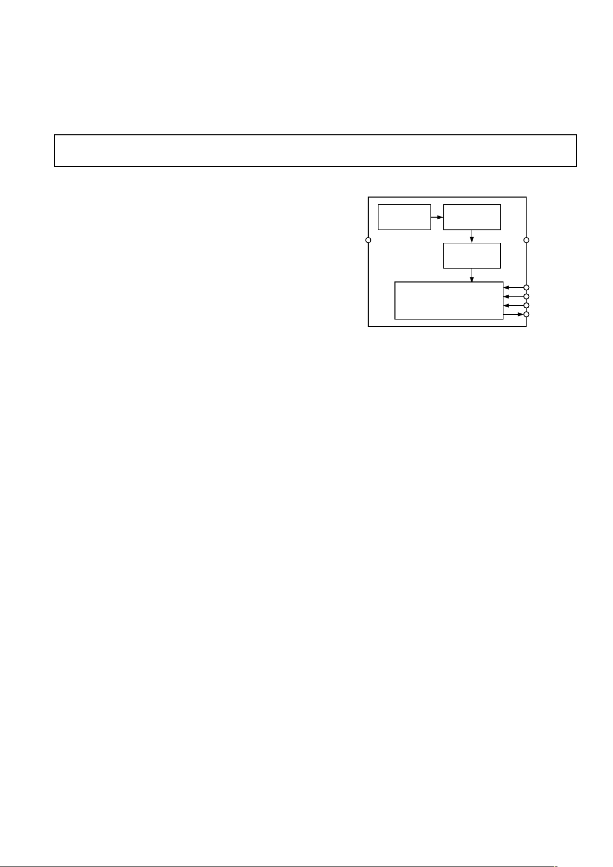
FUNCTIONAL BLOCK DIAGRAM
SERIAL
BUS
INTERFACE
AD7814
V
DD
CS
SCLK
DIN
DOUT
GND
TEMPERATURE
VALUE
REGISTER
10-BIT
ANALOG/DIGITAL
CONVERTER
BANDGAP
TEMPERATURE
SENSOR
FEATURES
10-Bit Temperature-to-Digital Converter
–55ⴗC to +125ⴗC Operating Temperature Range
ⴞ2ⴗC Accuracy
SPI- and DSP-Compatible Serial Interface
Shutdown Mode
Space-Saving SOT-23 Package
APPLICATIONS
Hard Disk Drives
Personal Computers
Electronic Test Equipment
Office Equipment
Domestic Appliances
Process Control
GENERAL DESCRIPTION
The AD7814 is a complete temperature monitoring system in
an SOT-23 package or 8-lead µSOIC package. It contains a
bandgap temperature sensor and 10-bit ADC to monitor and
digitize the temperature reading to a resolution of +0.25°C.
The AD7814 has a flexible serial interface that allows easy interfacing to most microcontrollers. The interface is compatible
with SPI™, QSPI and MICROWIRE™ protocol and is also
compatible with DSPs. The part features a standby mode that is
controlled via the serial interface.
The AD7814’s wide supply voltage range, low supply current
and SPI-compatible interface, make it ideal for a variety of applications, including personal computers, office equipment, and
domestic appliances.
SPI is a trademark of Motorola, Inc.
MICROWIRE is a trademark of National Semiconductor, Inc.
PRODUCT HIGHLIGHTS
1. The AD7814 has an on-chip temperature sensor that allows
an accurate measurement of the ambient temperature. The
measurable temperature range is –55°C to +125°C, with a
± 2°C temperature accuracy.
2. Supply voltage of +2.7 V to +5.5 V.
3. Space-saving 6-lead SOT-23 package and 8-lead µSOIC
package.
4. 10-bit temperature reading to +0.25°C resolution.
5. The AD7814 features a standby mode that reduces the
current consumption to 1 µA.
Page 2
REV. B
–2–
AD7814–SPECIFICATIONS
1, 2
Parameter Min Typ Max Units Test Conditions/Comments
TEMPERATURE SENSOR AND ADC
Accuracy ± 2.0 °CT
A
= 0°C to +85°C. VDD = +3 V to +5.5 V
3
± 2.5 °CT
A
= –40°C to 0°C. VDD = +3 V to +5.5 V
3
± 2.0 ± 3.5 °CT
A
= –55°C to +125°C. VDD = +3 V to +5.5 V
Resolution 10 Bits
Update Rate, t
R
400 µs
Temperature Conversion Time 25 µs
SUPPLIES
Supply Voltage 2.7 5.5 V For Specified Performance
Supply Current
Normal Mode 250 400 µA
Shutdown Mode 1 3 µA
Power Dissipation 80 µWV
DD
= +3 V. Using Normal Mode
Power Dissipation V
DD
= +3 V. Using Shutdown Mode
1 sps 3 µW
10 sps 3.3 µW
100 sps 6 µW
DIGITAL INPUT
Input High Voltage, V
IH
2.4 V
Input Low Voltage, V
IL
0.8 V
Input Current, I
IN
± 1 µAV
IN
= 0 V to V
DD
Input Capacitance, C
IN
10 pF All Digital Inputs
DIGITAL OUTPUT
Output High Voltage, V
OH
VDD – 0.3 V I
SOURCE
= I
SINK
= 200 µA
Output Low Voltage, V
OL
0.4 V IOL = 200 µA
Output Capacitance, C
OUT
50 pF
NOTES
1
All specifications apply for –55°C to +125°C unless otherwise stated.
2
Guaranteed by design and characterization, not production tested.
3
For VDD = +2.7 V to +3 V and TA = –40°C to +85°C, the typical temperature error is ±2°C.
Specifications subject to change without notice.
TIMING CHARACTERISTICS
1, 2, 3
Parameter Limit Units Comments
t
1
0 ns min CS to SCLK Setup Time
t
2
50 ns min SCLK High Pulsewidth
t
3
50 ns min SCLK Low Pulsewidth
t
4
4
35 ns max Data Access Time After SCLK Falling Edge
t
5
20 ns min Data Setup Time Prior to SCLK Rising Edge
t
6
0 ns min Data Hold Time After SCLK Rising Edge
t
7
0 ns min CS to SCLK Hold Time
t
8
4
40 ns max CS to DOUT High Impedance
NOTES
1
Guaranteed by design and characterization, not production tested.
2
All input signals are specified with tr = tf = 5 ns (10% to 90% of VDD) and timed from a voltage level of 1.6 V.
3
See Figure 2.
4
Measured with the load circuit of Figure 1.
(TA = T
MIN
to T
MAX
, VDD = +2.7 V to +5.5 V, unless otherwise noted)
(TA = T
MIN
to T
MAX
, VDD = +2.7 V to +5.5 V, unless otherwise noted)
Page 3

REV. B
AD7814
–3–
ORDERING GUIDE
Temperature Temperature Package Branding Package
Model Range Error* Description Information Option
AD7814ART –55°C to +125°C ± 2°C 6-Lead SOT-23 CAA RT-6
AD7814ARM –55°C to +125°C ± 2°C 8-Lead µSOIC CAA RM-8
*Temperature error is over 0°C to +85°C temperature range.
ABSOLUTE MAXIMUM RATINGS*
VDD to GND . . . . . . . . . . . . . . . . . . . . . . . . . . –0.3 V to +7 V
Digital Input Voltage to GND . . . . . . . –0.3 V to V
DD
+ 0.3 V
Digital Output Voltage to GND . . . . . –0.3 V to V
DD
+ 0.3 V
Operating Temperature Range . . . . . . . . . . –55°C to +125°C
Storage Temperature Range . . . . . . . . . . . . –65°C to +150°C
Junction Temperature . . . . . . . . . . . . . . . . . . . . . . . . +150°C
SOT-23, Power Dissipation . . . . . . . . . . . . . . . . . . . . 450 mW
θ
JA
Thermal Impedance . . . . . . . . . . . . . . . . . . . . 240°C/W
Lead Temperature, Soldering
Vapor Phase (60 sec) . . . . . . . . . . . . . . . . . . . . . +215°C
Infrared (15 sec) . . . . . . . . . . . . . . . . . . . . . . . . . +220°C
µSOIC Package, Power Dissipation . . . . . . . . . . . . . . 450 mW
θ
JA
Thermal Impedance . . . . . . . . . . . . . . . . . . . . 206°C/W
Lead Temperature, Soldering
Vapor Phase (60 sec) . . . . . . . . . . . . . . . . . . . . . +215°C
Infrared (15 sec) . . . . . . . . . . . . . . . . . . . . . . . . . +220°C
*Stresses above those listed under Absolute Maximum Ratings may cause perma-
nent damage to the device. This is a stress rating only; functional operation of the
device at these or any other conditions above those indicated in the operational
section of this specification is not implied. Exposure to absolute maximum rating
conditions for extended periods may affect device reliability.
CAUTION
ESD (electrostatic discharge) sensitive device. Electrostatic charges as high as 4000 V readily
accumulate on the human body and test equipment and can discharge without detection.
Although the AD7814 features proprietary ESD protection circuitry, permanent damage may
occur on devices subjected to high energy electrostatic discharges. Therefore, proper ESD
precautions are recommended to avoid performance degradation or loss of functionality.
WARNING!
ESD SENSITIVE DEVICE
+1.6V
I
OL
200A
200A
I
OH
TO
OUTPUT
PIN
C
L
50pF
Figure 1. Load Circuit for Data Access Time and Bus
Relinquish Time
Page 4

REV. B
AD7814
–4–
PIN FUNCTION DESCRIPTION
Pin SOT-23 SOIC
Mnemonic Pin No. Pin No. Description
GND 1 7 Analog and Digital Ground.
DIN 2 6 Serial Data Input. Serial data to be loaded to the part’s control register is
provided on this input. Data is clocked into the control register on the rising
edge of SCLK.
V
DD
3 5 Positive Supply Voltage, +2.7 V to +5.5 V.
SCLK 4 4 Serial Clock Input. This is the clock input for the serial port. The serial clock
is used to clock data out of the temperature value register of the AD7814 and
also to clock data into the control register on the part.
CS 5 3 Chip Select Input. Logic Input. The device is selected when this input is low.
The SCLK input is disabled when this pin is high.
DOUT 6 2 Serial Data Output. Logic output. Data is clocked out of the temperature
value register at this pin. Data is clocked out on the falling edge of SCLK.
NC 1, 8 No Connect.
PIN CONFIGURATIONS
SOT-23
1
2
3
GND
TOP VIEW
(Not to Scale)
6
5
4
AD7814
DIN
V
DD
DOUT
CS
SCLK
SOIC
TOP VIEW
(Not to Scale)
8
7
6
5
1
2
3
4
NC = NO CONNECT
NC
DOUT
CS
SCLK
NC
GND
DIN
V
DD
AD7814
Page 5

REV. B
AD7814
–5–
CIRCUIT INFORMATION
The AD7814 is a 10-bit digital temperature sensor. The part
houses an on-chip temperature sensor, a 10-bit A/D converter,
a reference and serial interface logic functions in an SOT-23
package. The A/D converter section consists of a conventional
successive-approximation converter based around a capacitor
DAC. The parts are capable of running on a +2.7 V to +5.5 V
power supply.
The on-chip temperature sensor allows an accurate measurement
of the ambient device temperature to be made. The working
measurement range of the AD7814 is –55°C to +125°C.
CONVERTER DETAILS
The conversion clock for the part is internally generated so no
external clock is required except when reading from and writing
to the serial port. In normal mode, an internal clock oscillator
runs the automatic conversion sequence. A conversion is initiated every 400 µs. At this time, the part wakes up and performs
a temperature conversion. This temperature conversion typically
takes 25 µs, at which time the part automatically shuts down.
The result of the most recent temperature conversion is available in the serial output register at any time. The AD7814 can
be placed in a shutdown mode, via the Control Register, in
which case, the on-chip oscillator is shut down and no further
conversions are initiated until the AD7814 is taken out of shutdown mode. The conversion result from the last conversion
prior to shutdown can still be read from the AD7814 even when
it is in shutdown mode.
In the automatic conversion mode, every time read or write
operation takes place, the internal clock oscillator is restarted at
the end of the read or write operation. The result of the conversion is available, typically 25 µs later. Similarly, when the
part is taken out of shutdown mode, the internal clock oscillator is restarted and the conversion result is available, typically
25 µs later. Reading from the device again before conversion is
complete will again provide the same set of data.
TEMPERATURE VALUE REGISTER
The temperature value register is a read-only register that stores
the temperature reading from the ADC in 10-bit twos complement format. The temperature data format is shown in Table I.
This shows the full theoretical range of the ADC from –128°C
to +127°C, but in practice the temperature measurement range
is limited to the operating temperature range of the device (–55°C
to +125°C). A typical performance curve is shown in Figure 7.
Table I. Temperature Data Format
Digital Output
Temperature DB9 . . . DB0
–128°C 10 0000 0000
–125°C 10 0000 1100
–100°C 10 0111 0000
–75°C 10 1101 0100
–50°C 11 0011 1000
–25°C 11 1001 1100
–0.25°C 11 1111 1111
0°C 00 0000 0000
+0.25°C 00 0000 0001
+10°C 00 0010 1000
+25°C 00 0110 0100
+50°C 00 1100 1000
+75°C 01 0010 1100
+100°C 01 1001 0000
+125°C 01 1111 0100
+127°C 01 1111 1100
SERIAL INTERFACE
The serial interface on the AD7814 consists of four wires, CS,
SCLK, DIN and DOUT. The interface can be operated in 3-wire
mode with DIN tied to Ground, in which case the interface has
read-only capability, with data being read from the data register
via the DOUT line. The DIN line is used to write the part into
standby mode, if required. The CS line is used to select the
device when more than one device is connected to the serial
clock and data lines.
The part operates in a slave mode and requires an externally
applied serial clock to the SCLK input to access data from the
data register. The serial interface on the AD7814 is designed to
allow the part to be interfaced to systems that provide a serial
clock that is synchronized to the serial data, such as the 80C51,
87C51, 68HC11, 68HC05 and PIC16Cxx microcontrollers as
well as DSP processors.
A read operation from the AD7814 accesses data from the
Temperature Value Register while a write operation to the part
writes data to the Control Register.
Page 6

REV. B
AD7814
–6–
Read Operation
Figure 2 shows the timing diagram for a serial read from the
AD7814. The CS line enables the SCLK input. Ten bits of data
are transferred during a read operation. Read operations occur
during streams of 16 clock pulses. The serial data is accessed in
a number of bytes if ten bits of data are being read. At the end
of the read operation, the DOUT line remains in the state of the
last bit of data clocked out of the AD7814 until CS returns
high, at which time the DOUT line goes into three-state.
Write Operation
Figure 2 also shows the timing diagram for a serial write to the
AD7814. The write operation takes place at the same time as
the read operation. Data is clocked into the Control Register on
the part on the rising edge of SCLK. Only the third bit in the
data stream provides a user-controlled function. This third bit is
the power-down bit which, when set to a 1, puts the AD7814
into shutdown mode. The first two bits of the data stream are
don’t cares while all other bits in the data stream other, than the
power-down bit, should be 0 to ensure correct operation of the
AD7814. Data is loaded to the Control Register on the fifteenth
falling SCLK edge and the data takes effect at this time i.e., if
the part is programmed to go into shutdown, it does so at this
point. If the CS is brought high before this fifteenth SCLK edge,
the Control Register will not be loaded and the power-down
status of the part will not change.
MICROPROCESSOR INTERFACING
The AD7814’s serial interface allows for easy interface to most
microcomputers and microprocessors. Figures 3 through 6 show
some typical interface circuits.
The serial interface on the AD7814 consists of four wires: CS,
DIN, DOUT and SCLK. All interface circuits shown utilize all
four interface lines. However, it is possible to operate the interface with three wires. If the application does not require the
power-down facility offered by the AD7814, the DIN line can
be tied permanently low. Thus, the interface can be operated
from just three wires, SCLK, CS, and DOUT.
CS
SCLK
DOUT
DIN
DON'T
CARE
DON'T
CARE
POWER-
DOWN
LEADING
ZERO
DB9 DB8 DB0
1 2 3 4 11 15 16
t
1
t
2
t
3
t
4
t
5
t
6
t
7
t
8
Figure 2. Serial Interface Timing Diagram
The serial data transfer to and from the AD7814 requires a
16-bit read operation. Many 8-bit microcontrollers have 8-bit
serial ports and this 16-bit data transfer is handled as two 8-bit
transfers. Other microcontrollers and DSP processors transfer
16 bits of data in a serial data operation.
AD7814 to MC68HC11 Interface
Figure 3 shows an interface between the AD7814 and the
MC68HC11 microcontroller. The MC68HC11 is configured in
the master mode with its CPOL bit set to a logic one and its
CPHA bit set to a logic one. When the MC68HC11 is configured like this, its SCLK line idles high between data transfers.
Data is transferred to and from the AD7814 in two 8-bit serial
data operations. The diagram shows the full (four-wire) interface. PC1 of the MC68HC11 is configured as an output and
used to drive the CS input.
AD7814*
SCLK
DOUT
DIN
CS
MC68HC11*
SCLK
MISO
MOSI
PC1
*ADDITIONAL PINS OMITTED FOR CLARITY
Figure 3. AD7814 to MC68HC11 Interface
AD7814 to 8051 Interface
An interface circuit between the AD7814 and the microcontroller is shown in Figure 3. The 8xC51 is configured in its
Mode 0 serial interface mode. The serial clock line of the 8xC51
(on P3.1) idles high between data transfers. Data is transferred
to and from the AD7814 in two 8-bit serial data operations. The
AD7814 outputs the MSB of its data stream as the first valid
bit while the 8xC51 expects the LSB first. Thus, the data read
into the serial buffer needs to be rearranged before the correct
data word from the AD7814 is available in the accumulator.
Page 7

REV. B
AD7814
–7–
In the example shown, the AD7814 is connected to the serial
port of the 8051. Because the serial interface of the 8xC51 contains only one data line, the DIN line of the AD7814 is tied low
in the interface example given in Figure 4.
For applications that require the use of the power-down feature
of the AD7814, the serial interface should be implemented
using data port lines on the 8051. This allows a full-duplex
serial interface to be implemented. The method involves ‘bitbanging’ a port line to generate a serial clock while using two
other port lines to shift data in and out with the fourth port line
connecting to CS. Port lines 1.0 through 1.3 (with P1.1 configured as an input) can be used to connect to SCLK, DOUT,
DIN and CS, respectively, to implement this scheme.
AD7814*
SCLK
DOUT
DIN
CS
8051*
P3.1
P3.0
P1.2
P1.3
*ADDITIONAL PINS OMITTED FOR CLARITY
Figure 4. AD7814 to 8051 Interface
AD7814 to PIC16C6x/7x Interface
Figure 5 shows an interface circuit between the AD7814 and the
PIC16C6x/7x microcontroller. The PIC16C6x/7x Synchronous
Serial Port (SSP) is configured as an SPI master with the Clock
Polarity bit set to a logic one. In this mode, the serial clock line
of the PIC16C6x/7x idles high between data transfers. Data is
transferred to and from the AD7814 in two 8-bit serial data
operations. In the example shown, port line RA1 is being used
to generate the CS for the AD7814.
AD7814*
SCLK
DOUT
DIN
CS
PIC16C6x/7x*
SCK
SDO
SDI
RA1
*ADDITIONAL PINS OMITTED FOR CLARITY
Figure 5. AD7814 to PIC16C6x/7x Interface
AD7814 to ADSP-21xx Interface
Figure 6 shows an interface between the AD7814 and the
ADSP-21xx DSP processor. To ensure correct operation of the
interface the SPORT Control Register should be set up as
follows:
TFSW = RFSW = 1, Alternate Framing
INVRFS = INVTFS = 1, Active Low Framing Signal
DTYPE = 00, Right Justify Data
SLEN = 1111, 16-Bit Data Words
ISCLK = 1, Internal Serial Clock
TFSR = RFS = 1, Frame Every Word
IRFS = 0, RFS Configured As Input
ITFS = 1, TFS Configured As Output
The interface requires an inverter between the SCLK line of the
ADSP-21xx and the SCLK input of the AD7814. The ADSP21xx has the TFS and RFS of the SPORT tied together with
TFS set as an output and RFS set as an input. The DSP operates
in Alternate Framing Mode and the SPORT Control Register is
set up as described above.
AD7814*
SCLK
DOUT
DIN
CS
ADSP-21xx*
SCK
DR
DT
RFS
*ADDITIONAL PINS OMITTED FOR CLARITY
TFS
Figure 6. AD7814 to ADSP-21xx Interface
MOUNTING THE AD7814
The AD7814 can be used for surface or air-temperature sensing
applications. If the device is cemented to a surface with thermally conductive adhesive, the die temperature will be within
about 0.1°C of the surface temperature, thanks to the device’s
low power consumption. Care should be taken to insulate the
back and leads of the device from the air, if the ambient air
temperature is different from the surface temperature being
measured.
The ground pin provides the best thermal path to the die, so the
temperature of the die will be close to that of the printed circuit
ground track. Care should be taken to ensure that this is in good
thermal contact with the surface being measured.
As with any IC, the AD7814 and its associated wiring and circuits must be kept free from moisture to prevent leakage and
corrosion, particularly in cold conditions where condensation is
more likely to occur. Water-resistant varnishes and conformal
coatings can be used for protection. The small size of the
AD7814 package allows it to be mounted inside sealed metal
probes, which provide a safe environment for the device.
SUPPLY DECOUPLING
The AD7814 should be decoupled with a 0.1 µF ceramic
capacitor between V
DD
and GND. This is particularly important
if the AD7814 is mounted remote from the power supply.
TEMPERATURE – ⴗC
–0.4
–55
TEMPERATURE ERROR
–0.2
0
0.2
0.4
0.6
0.8
1
–40 0 25 40 85 100 120
Figure 7. Typical AD7814 Temperature Error
Page 8

REV. B
AD7814
–8–
C3599a–0–5/00 (rev. B) 01041
PRINTED IN U.S.A.
OUTLINE DIMENSIONS
Dimensions shown in inches and (mm).
8-Lead Mini/Micro SOIC
(RM-8)
0.011 (0.28)
0.003 (0.08)
0.028 (0.71)
0.016 (0.41)
33ⴗ
27ⴗ
0.120 (3.05)
0.112 (2.84)
85
41
0.122 (3.10)
0.114 (2.90)
0.199 (5.05)
0.187 (4.75)
PIN 1
0.0256 (0.65) BSC
0.122 (3.10)
0.114 (2.90)
SEATING
PLANE
0.006 (0.15)
0.002 (0.05)
0.018 (0.46)
0.008 (0.20)
0.043 (1.09)
0.037 (0.94)
0.120 (3.05)
0.112 (2.84)
6-Lead Plastic Surface Mount SOT-23
(RT-6)
0.122 (3.10)
0.106 (2.70)
PIN 1
0.118 (3.00)
0.098 (2.50)
0.075 (1.90)
BSC
0.037 (0.95) BSC
1
3
4 5 6
2
0.071 (1.80)
0.059 (1.50)
0.009 (0.23)
0.003 (0.08)
0.022 (0.55)
0.014 (0.35)
10ⴗ
0ⴗ
0.020 (0.50)
0.010 (0.25)
0.059 (0.15)
0.000 (0.00)
0.051 (1.30)
0.035 (0.90)
SEATING
PLANE
0.057 (1.45)
0.035 (0.90)
 Loading...