

Page 1
a
+3.3 V to +5 V Quad/Octal 10-Bit DACs
AD7804/AD7805/AD7808/AD7809*
FEATURES
Four 10-Bit DACs in One Package
Serial and Parallel Loading Facilities Available
AD7804 Quad 10-Bit Serial Loading
AD7805 Quad 10-Bit Parallel Loading
AD7808 Octal 10-Bit Serial Loading
AD7809 Octal 10-Bit Parallel Loading
+3.3 V to +5 V Operation
Power-Down Mode
Power-On Reset
Standby Mode (All DACs/Individual DACs)
Low Power All CMOS Construction
10-Bit Resolution
Double Buffered DAC Registers
Dual External Reference Capability
APPLICATIONS
Optical Disk Drives
Instrumentation and Communication Systems
Process Control and Voltage Setpoint Control
Trim Potentiometer Replacement
Automatic Calibration
GENERAL DESCRIPTION
The AD7804/AD7808 are quad/octal 10-bit digital-to-analog
converters, with serial load capabilities, while the AD7805/AD7809
are quad/octal 10-bit digital-to-analog converters with parallel
load capabilities. These parts operate from a +3.3 V to +5 V
(±10%) power supply and incorporates an on-chip reference.
These DACs provide output signals in the form of V
is derived internally from V
V
SWING
. On-chip control registers
BIAS
BIAS
± V
SWING
.
include a system control register and channel control registers.
The system control register has control over all DACs in the
package. The channel control registers allow individual control
of DACs. The complete transfer function of each individual
DAC can be shifted around the V
point using an on-chip
BIAS
Sub DAC. All DACs contain double buffered data inputs,
which allow all analog outputs to be simultaneously updated
using the asynchronous LDAC input.
Control Features Channels Controlled Main DAC Sub DAC
Hardware Clear All 兹兹
System Control
Power Down
1
All 兹兹
System Standby2All 兹兹
System Clear All 兹
Input Coding All 兹兹
Channel Control
Channel Standby2Selective 兹兹
Channel Clear Selective 兹
V
BIAS
NOTES
1
Power-down function powers down all internal circuitry including the reference.
2
Standby functions power down all circuitry except for the reference.
Selective 兹兹
REV. A
Information furnished by Analog Devices is believed to be accurate and
reliable. However, no responsibility is assumed by Analog Devices for its
use, nor for any infringements of patents or other rights of third parties
which may result from its use. No license is granted by implication or
otherwise under any patent or patent rights of Analog Devices.
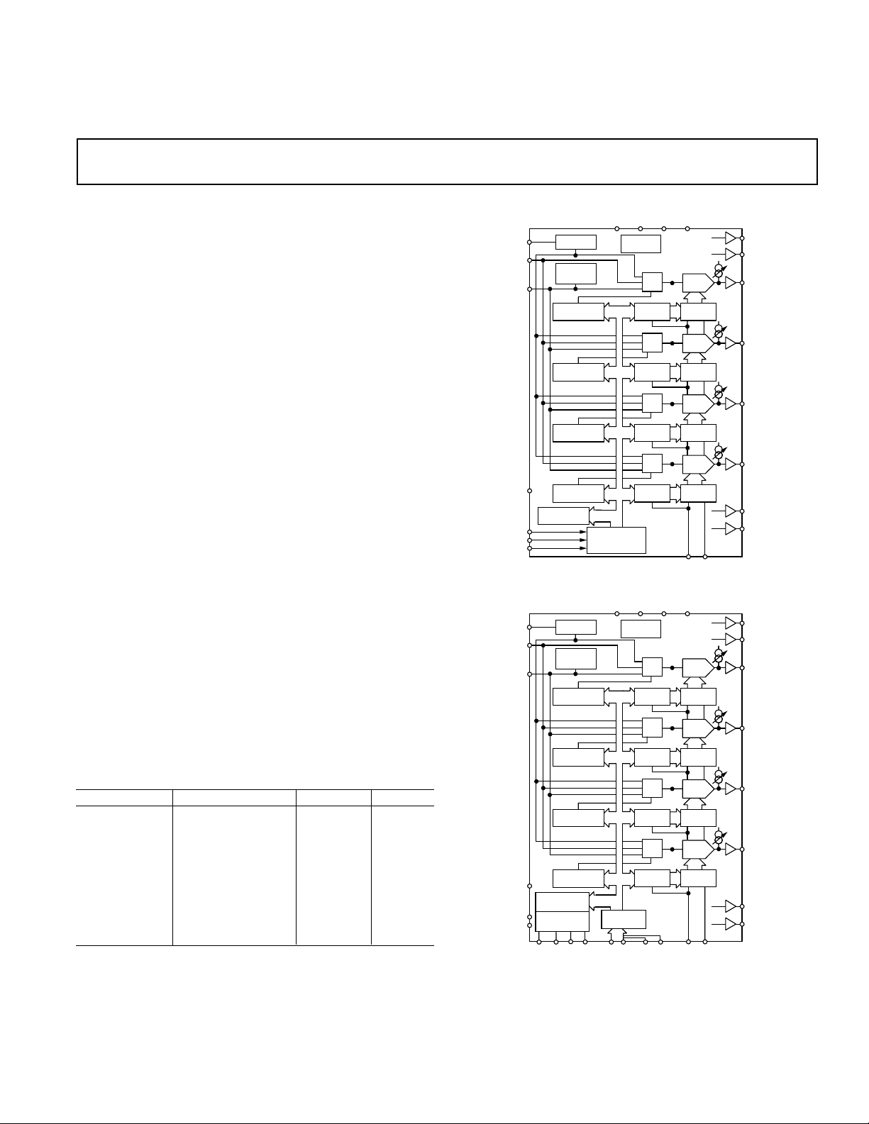
FUNCTIONAL BLOCK DIAGRAMS
AV
REFOUT
REFIN
COMP
PD**
FSIN
CLKIN
SDIN
REFOUT
REFIN
COMP
PD**
CS
WR
1.23V REF
AV
DD
DIVIDER
CHANNEL D
CONTROL REG
CHANNEL C
CONTROL REG
CHANNEL B
CONTROL REG
CHANNEL A
CONTROL REG
SYSTEM
CONTROL REG
**ONLY AD7804 SHOWN FOR CLARITY
**SHOWS ADDITIONAL CHANNELS ON THE AD7808
**PIN ON THE AD7808 ONLY
SYSTEM
CONTROL REG
CONTROL
LOGIC
MODE A0 A1 DB9 DB2 DB1 DB0
**ONLY AD7805 SHOWN FOR CLARITY
**SHOWS ADDITIONAL CHANNELS ON THE AD7809
**PIN ON THE AD7809 ONLY
CONTROL LOGIC
1.23V REF
AV
DD
DIVIDER
CHANNEL D
CONTROL REG
CHANNEL C
CONTROL REG
CHANNEL B
CONTROL REG
CHANNEL A
CONTROL REG
A2**
INPUT SHIFT
REGISTER &
AV
REGISTER
*Patent pending.
Index on Page 26.
One Technology Way, P.O. Box 9106, Norwood, MA 02062-9106, U.S.A.
Tel: 781/329-4700 World Wide Web Site: http://www.analog.com
Fax: 781/326-8703 © Analog Devices, Inc., 1998
DDDVDD
POWER ON
RESET
DDDVDD
POWER ON
RESET
INPUT
AGND DGND
MUX
DATA
REGISTER
MUX
DATA
REGISTER
MUX
DATA
REGISTER
MUX
DATA
REGISTER
AGND DGND
MUX
DATA
REGISTER
MUX
DATA
REGISTER
MUX
DATA
REGISTER
MUX
DATA
REGISTER
AD7804/
AD7808
V
BIAS
V
BIAS
V
BIAS
V
BIAS
AD7805/
AD7809
V
BIAS
V
BIAS
V
BIAS
V
BIAS
DAC D
DAC
REGISTER
DAC C
DAC
REGISTER
DAC B
DAC
REGISTER
DAC A
DAC
REGISTER
LDACCLR
DAC D
DAC
REGISTER
DAC C
DAC
REGISTER
DAC B
DAC
REGISTER
DAC A
DAC
REGISTER
LDACCLR
V
F*
OUT
V
E*
OUT
V
D
OUT
V
C
OUT
B
V
OUT
V
A
OUT
V
H*
OUT
V
G*
OUT
V
F*
OUT
V
E*
OUT
V
D
OUT
V
C
OUT
B
V
OUT
V
A
OUT
V
H*
OUT
V
G*
OUT
Page 2

AD7804/AD7805/AD7808/AD7809
AD7804/AD7805–SPECIFICATIONS
Reference = Internal Reference; CL = 100 pF; RL = 2 k⍀ to GND. Sub DAC at Midscale. All specifications T
Parameter B Grade
1
C Grade
(AVDD and DVDD = 3.3 V ⴞ 10% to 5 V ⴞ 10%; AGND = DGND = 0 V;
to T
MIN
1
Units Comments
unless otherwise noted.)
MAX
STATIC PERFORMANCE
MAIN DAC
Resolution 10 10 Bits
Relative Accuracy ±3 ±3 LSB max
Gain Error ±3 ±3 % FSR max
Bias Offset Error
Zero-Scale Error
Monotonicity 9 10 Bits and 200H for Twos Complement Coding
2
3
–80/+40 –80/+40 mV max DAC Code = 0.5 Full Scale
–V
BIAS
/ +40
16
–V
BIAS
/ +40
16
mV max DAC Code = 000H for Offset Binary
Minimum Load Resistance 2 2 kΩ min
SUB DAC
Resolution 8 8 Bits
Differential Nonlinearity ±0.125 ±0.125 LSB typ Refers to an LSB of the Main DAC
±0.5 ±0.5 LSB max
OUTPUT CHARACTERISTICS
Output Voltage Range
3
V
± 15/16 × V
BIAS
V
/16 to 31/16 × V
BIAS
BIAS
BIASVBIAS
V
± 15/16 × V
BIAS
/16 to 31/16 × V
BIAS
V Twos Complement Coding
V Offset Binary Coding
BIAS
Voltage Output Settling Time to 10 Bits 4 4 µs max Typically 1.5 µs
Slew Rate 2.5 2.5 V/µs typ
Digital-to-Analog Glitch Impulse 1 1 nV-s typ 1 LSB Change Around the Major Carry
Digital Feedthrough 0.5 0.5 nV-s typ
Digital Crosstalk 0.5 0.5 nV-s typ
Analog Crosstalk ±0.2 ±0.2 LSB typ
DC Output Impedance 2 2 Ω typ
Power Supply Rejection Ratio 0.002 0.002 %/% typ ∆VDD ± 10%
DAC REFERENCE INPUTS
REF IN Range 1.0 to VDD/2 1.0 to VDD/2 V min to V max
REF IN Input Leakage ±1 ±1 µA max Typically ±1 nA
DIGITAL INPUTS
Input High Voltage, VIH @ VDD = 5 V 2.4 2.4 V min
Input High Voltage, VIH @ VDD = 3.3 V 2.1 2.1 V min
Input Low Voltage, VIL @ VDD = 5 V 0.8 0.8 V max
Input Low Voltage, VIL @ VDD = 3.3 V 0.6 0.6 V max
Input Leakage Current ±10 µA max
Input Capacitance 10 10 pF max
Input Coding Twos Comp/Binary Twos Comp/Binary
REFERENCE OUTPUT
REF OUT Output Voltage 1.23 1.23 V nom
REF OUT Error ±8 ±8 % max
REF OUT Temperature Coefficient –100 –100 ppm/°C typ
REF OUT Output Impedance 5 5 kΩ nom
POWER REQUIREMENTS
VDD (AV
I
DD
and DVDD) 3/5.5 3/5.5 V min to V max
DD
(AI
Plus DIDD) Excluding Load Currents
DD
Normal Mode 12 12 mA max VIH = VDD, VIL = DGND
System Standby (SSTBY) Mode 250 250 µAV
= VDD, VIL = DGND
IH
Power-Down (PD) Mode
@ +25°C 0.8 0.8 µA max V
T
MIN–TMAX
1.5 1.5 µA max
= VDD, VIL = DGND
IH
Power Dissipation Excluding Power Dissipated in Load
Normal Mode 66 66 mW max
System Standby (SSTBY) Mode 1.38 1.38 mW max
Power-Down (PD) Mode
@ +25°C 4.4 4.4 µW max
T
MIN–TMAX
NOTES
1
Temperature range is – 40°C to +85°C.
2
Can be minimized using the Sub DAC.
3
V
is the center of the output voltage swing and can be VDD/2, Internal Reference or REFIN as determined by MX1 and MX0 in the channel control register.
BIAS
Specifications subject to change without notice.
8.25 8.25 µW max
REV. A–2–
Page 3

AD7804/AD7805/AD7808/AD7809
AD7808/AD7809–SPECIFICATIONS
Reference = Internal Reference; CL = 100 pF; RL = 2 k⍀ to GND. Sub DAC at Midscale. All specifications T
Parameter B Grade
1
(AVDD and DVDD = 3.3 V ⴞ 10% to 5 V ⴞ 10%; AGND = DGND = 0 V;
to T
MIN
Units Comments
unless otherwise noted.)
MAX
STATIC PERFORMANCE
MAIN DAC
Resolution 10 Bits
Relative Accuracy ±4 LSB max
Gain Error ±3 % FSR max
Bias Offset Error
2
±60 mV max DAC Code = 0.5 Full Scale
Zero-Scale Error ±35 mV max DAC Code = 000H for Offset Binary
Monotonicity 9 Bits and 200H for Twos Complement
Minimum Load Resistance 2 kΩ min Coding
SUB DAC
Resolution 8 Bits
Differential Nonlinearity ±0.125 LSB typ Refers to an LSB of the Main DAC
±0.5 LSB max
OUTPUT CHARACTERISTICS
Output Voltage Range
3
V
± 15/16 × V
BIAS
V
/16 to 31/16 × V
BIAS
BIAS
BIAS
V Twos Complement Coding
V Offset Binary Coding
Voltage Output Settling Time to 10 Bits 4 µs max Typically 1.5 µs
Slew Rate 2.5 V/µs typ
Digital-to-Analog Glitch Impulse 1 nV-s typ 1 LSB Change Around the Major Carry
Digital Feedthrough 0.5 nV-s typ
Digital Crosstalk 0.5 nV-s typ
Analog Crosstalk ±0.2 LSB typ
DC Output Impedance 2 Ω typ
Power Supply Rejection Ratio 0.002 %/% typ ∆V
DD
± 10%
DAC REFERENCE INPUTS
REF IN Range 1.0 to VDD/2 V min to V max
REF IN Input Leakage ±1 µA max Typically ±1 nA
DIGITAL INPUTS
Input High Voltage, VIH @ VDD = 5 V 2.4 V min
Input High Voltage, VIH @ VDD = 3.3 V 2.1 V min
Input Low Voltage, VIL @ VDD = 5 V 0.8 V max
Input Low Voltage, VIL @ VDD = 3.3 V 0.6 V max
Input Leakage Current ±10 µA max
Input Capacitance 8 pF max
Input Coding Twos Comp/Binary
REFERENCE OUTPUT
REF OUT Output Voltage 1.23 V nom
REF OUT Error ±8 % max
REF OUT Temperature Coefficient –100 ppm/°C typ
REF OUT Output Impedance 5 kΩ nom
POWER REQUIREMENTS
VDD (AV
I
DD
and DVDD) 3/5.5 V min to V max
DD
(AI
Plus DIDD) Excluding Load Currents
DD
Normal Mode 18 mA max VIH = VDD, VIL = DGND
System Standby (SSTBY) Mode 250 µA max V
= VDD, VIL = DGND
IH
Power-Down (PD) Mode
@ +25°C1µA max V
T
MIN–TMAX
3 µA max
= VDD, VIL = DGND
IH
Power Dissipation Excluding Power Dissipated in Load
Normal Mode 99 mW max
System Standby (SSTBY) Mode 1.38 mW max
Power-Down (PD) Mode
@ +25°C 5.5 µW max
T
MIN–TMAX
NOTES
1
Temperature range is – 40°C to +85°C.
2
Can be minimized using the Sub DAC.
3
V
is the center of the output voltage swing and can be VDD/2, Internal Reference or REFIN as determined by MX1 and MX0 in the channel control register.
BIAS
Specifications subject to change without notice.
16.5 µW max
REV. A
–3–
Page 4
AD7804/AD7805/AD7808/AD7809
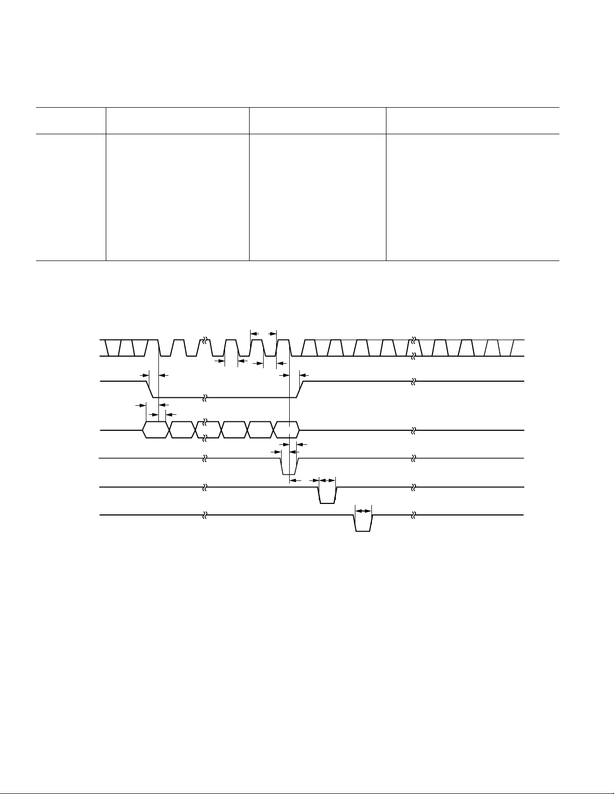
AD7804/AD7808 TIMING CHARACTERISTICS
Internal Reference. All specifications T
MIN
to T
unless otherwise noted.)
MAX
1
(V
= 3.3 V ⴞ 10% to 5 V ⴞ 10%; AGND = DGND = 0 V; Reference =
DD
Limit at T
MIN
, T
MAX
Parameter All Versions Units Description
t
1
t
2
t
3
t
4
t
5
t
6
t
6A
t
7
100 ns min CLKIN Cycle Time
40 ns min CLKIN High Time
40 ns min CLKIN Low Time
30 ns min FSIN Setup Time
30 ns min Data Setup Time
5 ns min Data Hold Time
6 ns min LDAC Hold Time
90 ns max FSIN Hold Time
20 ns min
t
8
t
9
NOTES
1
Sample tested during initial release and after any redesign or process change that may affect this parameter. All input signals are specified with tr = tf = 5 ns and
timed from a voltage of (VIL + VIH)/2.
Specifications subject to change without notice.
CLKIN(I)
FSIN(I)
SDIN(I) DB15
1
LDAC
2
LDAC
40 ns min LDAC, CLR Pulsewidth
100 ns min LDAC Setup Time
t
1
t
2
t
4
t
5
t
6
t
3
t
7
DB0
t
6A
t
5
t
9
t
8
t
CLR
1
TIMING REQUIREMENTS FOR SYNCHRONOUS LDAC UPDATE OR LDAC MAY BE TIED PERMANENTLY LOW IF REQUIRED.
2
TIMING REQUIREMENTS FOR ASYNCHRONOUS LDAC UPDATE.
8
Figure 1. Timing Diagram for AD7804 and AD7808
REV. A–4–
Page 5
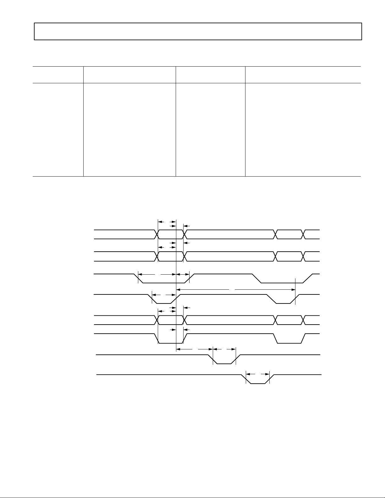
AD7805/AD7809 TIMING CHARACTERISTICS
= Internal Reference. All specifications T
MIN
to T
unless otherwise noted.)
MAX
AD7804/AD7805/AD7808/AD7809
1
(V
= 3.3 V ⴞ 10% to 5 V ⴞ 10%; AGND = DGND = 0 V; Reference
DD
Limit at T
MIN
, T
MAX
Parameter All Versions Unit Description
t
1
t
2
t
3
t
4
t
5
t
6
t
6A
t
7
t
8
t
9
t
10
t
11
t
12
NOTE
1
Sample tested during initial release and after any redesign or process change that may affect this parameter. All input signals are specified with tr = tf = 5 ns and
timed from a voltage of (VIL + VIH)/2.
Specifications subject to change without notice.
MODE
A0, A1, A2
25 ns min Mode Valid to Write Setup Time
4.5 ns min Mode Valid to Write Hold Time
25 ns min Address Valid to Write Setup Time
4.5 ns min Address Valid to Write Hold Time
25 ns min Data Setup Time
4.5 ns min Data Hold Time
6 ns min LDAC Valid to Write Hold Time
40 ns min Chip Select to Write Setup Time
0 ns min Chip Select to Write Hold Time
40 ns min Write Pulsewidth
100 ns min Time Between Successive Writes
40 ns min LDAC, CLR Pulsewidth
100 ns min Write to LDAC Setup Time
t
1
t
2
t
4
t
3
DATA
LDAC
LDAC
CLR
t
t
CS
WR
1
2
1
TIMING REQUIREMENTS FOR SYNCHRONOUS LDAC UPDATE OR LDAC MAY BE TIED PERMANENTLY LOW IF REQUIRED.
2
TIMING REQUIREMENTS FOR ASYNCHRONOUS LDAC UPDATE.
7
t
9
8
t
10
t
6
t
5
t
6A
t
12
t
11
t
11
Figure 2. Timing Diagram for AD7805/AD7809 Parallel Write
–5–REV. A
Page 6

AD7804/AD7805/AD7808/AD7809
WARNING!
ESD SENSITIVE DEVICE
ABSOLUTE MAXIMUM RATINGS
(T
= +25°C unless otherwise noted)
A
1
DVDD to DGND . . . . . . . . . . . . . . . . . . . . . . . . –0.3 V to +7 V
to AGND . . . . . . . . . . . . . . . . . . . . . . . . –0.3 V to +7 V
AV
DD
AGND to DGND . . . . . . . . . . . . . . . . . . . . . . . –0.3 V + 0.3 V
Digital Input Voltage to DGND . . . . . –0.3 V to DV
Analog Input Voltage to AGND . . . . . –0.3 V to AV
COMP to AGND . . . . . . . . . . . . . . . –0.3 V to AV
REF OUT to AGND . . . . . . . . . . . . . . . . . . –0.3 V to + AV
+ 0.3 V
DD
+ 0.3 V
DD
+ 0.3 V
DD
DD
REF IN to AGND . . . . . . . . . . . . . . . –0.3 V to AVDD + 0.3 V
to AGND2 . . . . . . . . . . . . . . . . –0.3 V to AVDD + 0.3 V
V
OUT
Input Current to Any Pin Except Supplies
3
. . . . . . . . ±10 mA
Operating Temperature Range
AD7804/AD7805 Commercial Plastic
(B, C Versions) . . . . . . . . . . . . . . . . . . . . –40°C to +85°C
AD7808/AD7809 Commercial Plastic
(B, C Versions) . . . . . . . . . . . . . . . . . . . . –40°C to +85°C
Storage Temperature Range . . . . . . . . . . . . –65°C to +150°C
Junction Temperature . . . . . . . . . . . . . . . . . . . . . . . . . +150°C
SOIC (R-16) Package, Power Dissipation . . . . . . . . . 450 mW
Thermal Impedance . . . . . . . . . . . . . . . . . . . . . . 75°C/W
θ
JA
Lead Temperature, Soldering
Vapor Phase (60 sec) . . . . . . . . . . . . . . . . . . . . . . +215°C
Infrared (15 sec) . . . . . . . . . . . . . . . . . . . . . . . . . . +220°C
PDIP (N-16) Package, Power Dissipation . . . . . . . . . 670 mW
Thermal Impedance . . . . . . . . . . . . . . . . . . . . . 116°C/W
θ
JA
Lead Temperature, Soldering (10 sec) . . . . . . . . . . . +260°C
SOIC (R-24) Package, Power Dissipation . . . . . . . . . 450 mW
Thermal Impedance . . . . . . . . . . . . . . . . . . . . . . 75°C/W
θ
JA
Lead Temperature, Soldering
Vapor Phase (60 sec) . . . . . . . . . . . . . . . . . . . . . . +215°C
Infrared (15 sec) . . . . . . . . . . . . . . . . . . . . . . . . . . +220°C
PDIP (N-24) Package, Power Dissipation . . . . . . . . . 670 mW
Thermal Impedance . . . . . . . . . . . . . . . . . . . . . 105°C/W
θ
JA
Lead Temperature, Soldering (10 sec) . . . . . . . . . . . +260°C
SOIC (R-28) Package, Power Dissipation . . . . . . . . . 875 mW
Thermal Impedance . . . . . . . . . . . . . . . . . . . . . . 70°C/W
θ
JA
Lead Temperature, Soldering
Vapor Phase (60 sec) . . . . . . . . . . . . . . . . . . . . . . +215°C
Infrared (15 sec) . . . . . . . . . . . . . . . . . . . . . . . . . . +220°C
PDIP (N-28) Package, Power Dissipation . . . . . . . . . 875 mW
Thermal Impedance . . . . . . . . . . . . . . . . . . . . . . 75°C/W
θ
JA
Lead Temperature, Soldering (10 sec) . . . . . . . . . . . +260°C
SSOP (RS-28) Package, Power Dissipation . . . . . . . . 875 mW
Thermal Impedance . . . . . . . . . . . . . . . . . . . . . 110°C/W
θ
JA
Lead Temperature, Soldering
Vapor Phase (60 sec) . . . . . . . . . . . . . . . . . . . . . . +215°C
Infrared (15 sec) . . . . . . . . . . . . . . . . . . . . . . . . . . +220°C
TQFP (ST-44B) Package, Power Dissipation . . . . . . 450 mW
Thermal Impedance . . . . . . . . . . . . . . . . . . . . . 116°C/W
θ
JA
Lead Temperature, Soldering
Vapor Phase (60 sec) . . . . . . . . . . . . . . . . . . . . . . +215°C
Infrared (15 sec) . . . . . . . . . . . . . . . . . . . . . . . . . . +220°C
NOTES
1
Stresses above those listed under Absolute Maximum Ratings may cause perma-
nent damage to the device. This is a stress rating only; functional operation of the
device at these or any other conditions above those listed in the operational
sections of this specification is not implied. Exposure to absolute maximum rating
conditions for extended periods may affect device reliability.
2
The outputs may be shorted to voltages in this range provided the power dissipation
of the package is not exceeded.
3
Transient currents of up to 100 mA will not cause SCR latch-up.
ORDERING GUIDE
Supply Temperature Relative Package
Model Voltage Range Accuracy Package Descriptions Options
AD7804BN 3.3 V to 5 V –40°C to +85°C ±3 LSB 16-Lead Plastic DIP N-16
AD7804BR 3.3 V to 5 V –40°C to +85°C ±3 LSB 16-Lead Small Outline IC R-16
AD7805BN 3.3 V to 5 V –40°C to +85°C ±3 LSB 28-Lead Plastic DIP N-28
AD7805BR 3.3 V to 5 V –40°C to +85°C ±3 LSB 28 Lead Small Outline IC R-28
AD7805BRS 3.3 V to 5 V –40°C to +85°C ±3 LSB 28-Lead Shrink Small Outline Package RS-28
AD7805CR 3.3 V to 5 V –40°C to +85°C ±3 LSB 28-Lead Small Outline IC R-28
AD7808BN 3.3 V to 5 V –40°C to +85°C ±4 LSB 24-Lead Plastic DIP N-24
AD7808BR 3.3 V to 5 V –40°C to +85°C ±4 LSB 24 Lead Small Outline IC R-24
AD7809BST 3.3 V to 5 V –40°C to +85°C ±4 LSB 44-Lead Thin Plastic Quad Flatpack (TQFP) ST-44B
CAUTION
ESD (electrostatic discharge) sensitive device. Electrostatic charges as high as 4000 V readily
accumulate on the human body and test equipment and can discharge without detection.
Although these devices feature proprietary ESD protection circuitry, permanent damage may
occur on devices subjected to high energy electrostatic discharges. Therefore, proper ESD
precautions are recommended to avoid performance degradation or loss of functionality.
REV. A–6–
Page 7
AD7804/AD7805/AD7808/AD7809
AD7804/AD7808 PIN FUNCTION DESCRIPTION
AD7804 AD7808
Pin No. Pin No. Mnemonic Description
1 1, 6 AGND Ground reference point for analog circuitry.
2, 3 2, 3 V
4 4 REFOUT Reference Output. This is a bandgap reference and is typically 1.23 V.
5 PD Active low input used to put the part into low power mode reducing current consumption
7, 8 V
59FSIN Level-triggered control input (active low). This is the frame synchronization signal for the
610LDAC LDAC Input. When this digital input is taken low, all DAC registers are simultaneously
7 11 SDIN Serial Data Input. These devices accept a 16-bit word. Data is clocked into the input shift
8 12 DGND Ground reference point for digital circuitry.
913DV
10 14 CLKIN Clock Input. Data is clocked into the input shift register on the falling edges of CLKIN.
11 15 CLR Asynchronous CLR Input. When this input is taken low, all Main DAC outputs are
16 NC No Connect. This pin should be left open circuit.
17, 18 V
12 20 REFIN This is an external reference input for the DACs. When this reference is selected for a
13 21 COMP Compensation Pin. This pin provides an output from the internal V
14, 15 22, 23 V
16 19, 24 AV
OUT
OUT
OUT
OUT
DD
DD
B, V
F, V
H, V
D, V
A Analog output voltage from the DACs.
OUT
to 1 µA.
E Analog output voltages from the DACs.
OUT
input data. When FSIN goes low, it enables the input shift register and data is transferred
on the falling edges of CLKIN.
updated with the contents of the data registers. If LDAC is tied permanently low, or is
low on the sixteenth falling clock edge with timing similar to that of SDIN, an automatic
update will take place.
register on the falling edge of CLKIN.
Digital Power Supply.
Duty Cycle should be between 40% and 60%.
cleared either to V
BIAS
or to V
BIAS
transfer function of the Main DAC will remain centered around the V
G Analog output voltages from the DACs.
OUT
DAC in the control register, the analog output from the selected DAC swings around this
point.
provided for ac bypass purposes only. This pin should be decoupled with 1 nF capacitors
to both AV
and AGND. This pin can be overdriven with an external reference, thus
DD
giving the facility for two external references on the part.
C Analog output voltage from the DACs.
OUT
Analog Power Supply. +3.3 V to +5 V.
/16 volts. All Sub DACs are also cleared and thus the
point.
BIAS
/2 divider and is
DD
AD7804 PIN CONFIGURATION
AGND
V
OUT
V
OUT
REFOUT
FSIN
LDAC
SDIN
DGND
1
B
2
3
A
4
5
6
7
8
AD7804
TOP VIEW
(Not to Scale)
16
15
14
13
12
11
10
9
AV
DD
V
OUT
V
OUT
COMP
REFIN
CLR
CLKIN
DV
DD
C
D
AD7808 PIN CONFIGURATION
AGND
V
OUT
V
OUT
REFOUT
AGND
V
OUT
V
OUT
FSIN
LDAC
SDIN
DGND
1
2
B
3
A
4
5
PD
AD7808
6
TOP VIEW
(Not to Scale)
7
F
8
E
9
10
11
12
NC = NO CONNECT
24
AV
DD
23
V
C
OUT
22
D
V
OUT
21
COMP
20
REFIN
19
AV
DD
18
V
G
OUT
17
V
H
OUT
16
NC
15
CLR
14
CLKIN
13
DV
DD
–7–REV. A
Page 8
AD7804/AD7805/AD7808/AD7809
44 43 42 41 40 39 38 37 36 35 34
1
2
3
4
5
6
7
8
9
10
11
12 13 14 15 16 17 18 19 20 21 22
33
32
31
30
29
28
27
26
25
24
23
PIN 1
IDENTIFIER
TOP VIEW
(Not to Scale)
NC = NO CONNECT
NC
REFIN
MODE
A0
A1
AV
DD
A2
DB0
V
OUT
G
DB1
DB2
NC
AGND
DB9
DB8
AGND
DB7
DB6
V
OUT
F
DB5
DB4
NC
PD
REFOUT
V
OUT
A
V
OUT
B
AGND
AGND
AV
DD
V
OUT
E
NC
LDAC
DB3
DV
DD
WR
CLR
NC
CS
V
OUT
H
DGND
AV
DD
V
OUT
C
V
OUT
D
COMP
AD7809
AD7805/AD7809 PIN FUNCTION DESCRIPTIONS
AD7805 AD7809
Pin No. Pin No. Mnemonic Description
1, 11, 13, NC No Connect. These pins should be left open circuit.
20, 33
1 2, 5, 39, 40 AGND Ground reference point for analog circuitry.
2, 3 41, 42 V
4 43 REFOUT Reference Output. This is a bandgap reference and is typically 1.23 V.
5–10, 3, 4, 6, 7, 9, DB9–DB2 Data Inputs. DB9 to DB2 are the 8 MSBs of the data word.
12, 13 10, 15, 23
19, 20 24, 26 DB1, DB0 DB1 and DB0 function as the 2 LSBs of the 10-bit word in 10-bit parallel mode but
8, 12 V
11 14 LDAC LDAC Input. When this digital input is taken low, all DAC registers are simultaneously
14 16 DGND Ground reference point for digital circuitry.
15 17 DV
16 18 WR Write Input WR is an active low logic input which is used in conjunction with CS and
17 21 CS Chip Select. Active low logic input.
18 19 CLR Asynchronous CLR Input. When this input is taken low, all Main DAC outputs are
22, 25 V
21, 22 27, 29, 30 A2, A1, A0 DAC Address Inputs. These digital inputs are used in conjunction with CS and WR to
23 31 MODE Logic Input. Logic high enables writing to the DAC data registers, a logic low enables
24 32 REFIN This is an external reference input for the DAC. When this reference is selected for the DAC
25 34 COMP Compensation Pin. This pin provides an output from the internal V
26, 27 35, 36 V
28 28, 37, 38 AV
44 PD Active low input used to put the part into low power mode reducing current consump-
OUT
OUT
OUT
OUT
DD
DD
B, V
F, V
H, V
D, V
A Analog output voltages from the DACs.
OUT
have other functions when BYTE loading structure is used.
E Analog output voltages from the DACs.
OUT
updated with the contents of the DAC data registers. If LDAC is permanently tied low, or is
low during the rising edge of WR similar to data inputs, an automatic update will take place.
Digital Power Supply.
the address pins to write data to the relevant registers.
cleared either to V
BIAS
or to V
BIAS
transfer function of the MAIN DAC will remain centered around the V
G Analog output voltages from the DACs.
OUT
determine which DAC channel control register or DAC data register is loaded from the
input register. These address bits are don’t cares when writing to the system control register.
writing to the control registers.
in the control register, the analog output from the selected DAC swings around this point.
provided for ac bypass purposes only. This pin should be decoupled with 1 nF capacitors
to both AV
and AGND. This pin can be overdriven with an external reference, thus
DD
giving the facility for two external references on the part.
C Analog output voltages from the DACs.
OUT
Analog Power Supply.
tion to 1 µA.
/16 volts. All Sub DACs are also cleared and thus the
point.
BIAS
/2 divider and is
DD
AD7805 PIN CONFIGURATION
1
AGND
2
B
V
OUT
3
V
A
OUT
DB9
DB8
DB7
DB6
DB5
DB4
LDAC
DB3
DB2
DGND
4
5
6
AD7805
7
TOP VIEW
(Not to Scale)
8
9
10
11
12
13
14
REFOUT
AD7809 PIN CONFIGURATION
28
AV
DD
27
V
C
OUT
V
D
26
OUT
25
COMP
24
REFIN
MODE
23
A0
22
A1
21
DB0
20
DB1
19
18
CLR
17
CS
16
WR
15
DV
DD
REV. A–8–
Page 9
AD7804/AD7805/AD7808/AD7809
TERMINOLOGY
Relative Accuracy
For the DACs, relative accuracy or endpoint nonlinearity is a
measure of the maximum deviation, in LSBs, from a straight
line passing through the endpoints of the DAC transfer function. Figures 32 and 33 show the linearity at 3 V and 5 V
respectively.
Differential Nonlinearity
Differential nonlinearity is the difference between the measured
change and the ideal 1 LSB change between any two adjacent
codes. A specified differential nonlinearity of ±1 LSB maxi-
mum ensures monotonicity.
Bias Offset Error
If the DACs are ideal, the output voltage of any DAC with
midscale code loaded will be equal to V
BIAS
where V
BIAS
is selected by MX1 and MX0 in the control register. The DAC bias
offset error is the difference between the actual output voltage
and V
, expressed in mV.
BIAS
Gain Error
The difference between the actual and ideal analog output
range, expressed as a percent of full-scale range. It is the deviation in slope of the DAC transfer characteristic from ideal.
Zero-Scale Error
The zero-scale error is the actual output minus the ideal output
from any DAC when zero code is loaded to the DAC. If offset
binary coding is used, the code loaded is 000Hex, and if twos
complement coding is used, a code of 200HEX is loaded to the
DAC to calculate the zero-scale error. Zero-scale error is expressed in mV.
Digital-to-Analog Glitch Impulse
Digital-to-analog glitch impulse is the impulse injected into the
analog output when the digital inputs change state with the
DAC selected and the LDAC used to update the DAC. It is
normally specified as the area of the glitch in nV-s and is measured when the digital input code is changed by 1 LSB at the
major carry transition. Regardless of whether offset binary or twos
complement coding is used, the major carry transition occurs at
the analog output voltage change of V
BIAS
to V
– 1 LSB
BIAS
or vice versa.
Digital Feedthrough
Digital feedthrough is a measure of the impulse injected into
the analog output of a DAC from the digital inputs of the same
DAC but is measured when the DAC is not updated. It is specified in nV secs and is measured with a full-scale code change on
the data bus, i.e., from all 0s to all 1s and vice versa.
Digital Crosstalk
Digital crosstalk is the glitch impulse transferred to the output
of one converter due to a digital code change to another DAC.
It is specified in nV-s.
Analog Crosstalk
Analog crosstalk is a change in output of any DAC in response
to a change in the output of one or more of the other DACs. It
is measured in LSBs.
Power Supply Rejection Ratio (PSRR)
This specification indicates how the output of the DAC is affected by changes in the power supply voltage. Power-supply
rejection ratio is quoted in terms of % change in output per %
change in V
for full-scale output of the DAC. VDD is varied
DD
±10%.
AD7804/AD7808 INTERFACE SECTION
The AD7804 and AD7808 are serial input devices. Three lines
control the serial interface, FSIN, CLKIN and SDIN. The timing
diagram is shown in Figure 1.
Two mode bits (MD1 and MD0) which are DB13 and DB14 of
the serial word written to the AD7804/AD7808 are used to determine whether writing is to the DAC data registers or the control
registers of the device. These parts contain a system control
register for controlling the operation of all DACs in the package
as well as a channel control register for controlling the operation of
each individual DAC. Table I shows how to access these registers.
Table I. Register Selection Table for the AD7804/AD7808
MD1 MD0 Function
0 0 Write enable to system control register.
0 1 Write enable to channel control register.
1 X Write enable to DAC data registers.
When the FSIN input goes low, data appearing on the SDIN
line is clocked into the input register on each falling edge of
CLKIN. Data to be transferred to the AD7804/AD7808 is
loaded MSB first. Figure 4 shows the loading sequence for the
AD7804/AD7808 system control register, Figure 5 shows the
sequence for the channel control register write, and Figures 6
and 7 show the sequence for loading data to the Main and Sub
DAC data registers. Figure 3 shows the internal registers associated with the AD7804/AD7808 serial interface DACs. Only one
DAC structure is shown for clarity.
FSIN
CLKIN
SDIN
DATA REGISTER
8
DAC REGISTER
8
8-BIT DAC
(SUB DAC)
SYSTEM
CONTROL
REGISTER
TO ALL
CHANNELS
SINGLE
CHANNEL
INTERNAL V
REFIN
V
OUT
REF
VDD/2
16-BIT
INPUT SHIFT REGISTER
DECODER
CHANNEL
CONTROL
REGISTER
MUX
V
BIAS
DATA REGISTER
DAC REGISTER
10
10
10-BIT DAC
(MAIN DAC)
Figure 3. AD7804/AD7808 Internal Registers
–9–REV. A
Page 10

AD7804/AD7805/AD7808/AD7809
MSB LSB
X MD0 = 0MD1 = 0XXXXX0 BIN/COMP PD SSTBY SCLR 0 X X
X = Don’t Care
Figure 4. AD7804/AD7808 System Control Register Loading Sequence
DB15 (MSB) DB0 (LSB)
X MD0 = 1 MD1 = 0 A2* A1 A0 MX1 MX0 X X X STBY CLR 0 X X
X = Don’t Care
*Applicable to the AD7808 Only, and Are Don’t Care Conditions when Operating the AD7804 .
Figure 5. AD7804/AD7808 Channel Control Register Loading Sequence
DB15 (MSB) DB0 (LSB)
MAIN/SUB MD0 = X MD1 = 1 A2* A1 A0 DB9 DB8 DB7 DB6 DB5 DB4 DB3 DB2 DB1 DB0
X = Don’t Care
*Applicable to the AD7808 Only, and Are Don’t Care Conditions when Operating the AD7804 .
Figure 6. AD7804/AD7808 Main DAC Data Register Loading Sequence (
DB15 (MSB) DB0 (LSB)
MAIN/SUB MD0 = X MD1 = 1 A2* A1 A0 DB7 DB6 DB5 DB4 DB3 DB2 DB1 DB0 X X
X = Don’t Care
*Applicable to the AD7808 Only, and Are Don’t Care Conditions when Operating the AD7804.
Figure 7. AD7804/AD7808 Sub DAC Data Register Loading Sequence (
MAIN
MAIN
/SUB = 0)
/SUB = 1)
When the system control register is selected by writing zeros to
the mode bits, MD1 and MD0 the address bits are ignored as
the system control register controls all DACs in the package.
When MD1 = 0 and MD0 = 1, writing is to the channel control
register. Only the DAC selected by the address bits will be affected by writing to this register. Each individual DAC has a
channel control register.
The DACs data registers are addressed by writing a one to
MD1 (DB13); the condition of MD0 (DB14) does not matter
when writing to the data registers. DB15 determines whether
writing is to the Main DAC data register or to the Sub DAC
data register. The Main DAC is 10 bits wide and the Sub DAC
is 8 bits wide. Thus when writing to the Sub DAC DB1 and
DB0 become don’t cares. The Sub DAC is used to offset the
complete transfer function of the Main DAC around its V
BIAS
point. The Sub DAC has 1/8 LSB resolution and will enable the
transfer function of the Main DAC to be offset by ± V
BIAS
/32.
When the LDAC line goes low, all DAC registers in the device
are simultaneously loaded with the contents of their respective
DAC data registers, and the outputs change accordingly.
Bringing the CLR line low resets the DAC data and DAC registers. This hardware clear affects both the Main and Sub DACs.
This operation sets the analog output of the Main DAC to V
BIAS
/
16 when offset binary coding is selected and the output is set to
when twos complement coding is used. V
V
BIAS
is the output
BIAS
of the internal multiplexer as shown in Figure 3. The output of
the Sub DAC is used to shift the transfer function of the Main
DAC around the V
point and the contribution from the Sub
BIAS
DAC is zero following an external hardware clear. Software
clears affect the Main DACs only.
AD7804/AD7808 SYSTEM CONTROL REGISTER (MD1 = 0,
MD0 = 0)
The bits in this register allow control over all DACs in the
package. The control bits include power down (PD), DAC input
coding select (BIN/COMP), system standby (SSTBY) and a
system clear (SCLR). The function of these bits is as follows:
Power Down (PD)
This bit in the control register is used to shut down the complete
device. With a 0 in this position, the reference and all DACs are
put into low power mode. Writing a 1 to this bit puts the part in
the normal operating mode. When in power-down mode, the
contents of all registers are retained and are valid when the
device is put back into normal operation.
Coding (BIN/COMP)
This bit in the system control register allows the user to select
one of two input coding schemes. The available schemes are
Twos complement coding and offset binary coding. All DACs
will be configured with the same input coding scheme. Writing
a zero to the control register selects twos complement coding,
while writing a 1 to this bit in the control register selects offset
binary coding.
With twos complement coding selected the output voltage from
the Main DAC is of the form :
V
OUT=VBIAS±VSWING
where
V
SWING
15
is
×V
BIAS
16
With Offset Binary coding selected the output voltage from the
Main DAC ranges from:
V
OUT
V
BIAS
=
16
to V
OUT
31
V
=
×
BIAS
16
REV. A–10–
Page 11

V
can be the internal bandgap reference, the internal VDD/2
BIAS
reference or the external REFIN as determined by MX1 and
MX0 in the channel control register. A second external reference can be used if required by overdriving the V
/2 reference
DD
which appears at the COMP pin.
System Standby (SSTBY)
This bit allows all the DACs in the package to be put into low
power mode simultaneously but the reference is not affected.
Writing a one to the SSTBY bit in the system control register
puts all DACs into standby mode. On writing a one to this bit
all linear circuitry is switched off and the DAC outputs are
connected through a high impedance to ground. The DACs come
out of standby mode when a 0 is written to the SSTBY bit.
System Clear Function (SCLR)
This function allows the user to clear the contents of all data
and DAC registers in software. Writing a one to the SCLR bit
in the control register clears the DAC’s outputs. A zero in this
bit position puts the DAC in normal operating mode. The output of the Main DACs are cleared to one of two voltages depending on the input coding used. If twos complement coding
is selected, then issuing a software clear will reset the output of
the Main DAC to midscale (V
selected, the Main DAC output will be reset to V
). If offset binary coding is
BIAS
/16 follow-
BIAS
ing the execution of a software clear. This system clear function
does not affect the Sub DAC; the Sub DAC data register retains
its value during a system software clear (SCLR).
AD7804/AD7805/AD7808/AD7809
Standby (STBY)
This bit allows the selected DAC in the package to be put into
low power mode. Writing a zero to the STBY bit in the channel
control register puts the selected DAC into standby mode. On
writing a zero to this bit all linear circuitry is switched off and
the DAC output is connected through a high impedance to
ground. The DAC is returned to normal operation by writing a
one to the STBY bit.
Software Clear Function (CLR)
This function allows the user to clear the contents of the selected DAC’s data in software. Writing a one to the CLR bit in
the control register clears the DAC’s output. A zero in the CLR
bit position puts the DAC in normal operating mode. This
software CLR operation clears only the Main DAC, the contents of the Sub DAC is unaffected by a CLR operation. The
output of the Main DAC can be cleared to one of two places
depending on the input coding used. An LDAC pulse is required to activate the channel clear function and must be applied after the bit in the channel control register is set or reset. If
twos complement coding is selected, then issuing a software
clear will reset the output of the Main DAC to midscale (V
If offset binary coding is selected, the Main DAC output will be
reset to V
Multiplexer Selection (MX1, MX0)
/16 following the execution of a software clear.
BIAS
These two bits are used to select the reference input for the
selected DAC. Table III shows the options available.
BIAS
).
AD7804/AD7808 CHANNEL CONTROL REGISTER (MD1 = 0,
MD0 = 1)
This register allows the user to have control over individual
DACs in the package. The control bits in this register include
the address bits for the selected DAC, standby (STBY), individual DAC clear (CLR) and multiplexer output selection
(MX1 and MX0). The function of these bits follows.
DAC Selection (A2, A1, A0)
Bits A2, A1 and A0 in the input registers are used to address a
specific DAC. Table IIa shows the selection table for the DACs
of the AD7804. Table IIb shows the selection table for the
DACs of the AD7808.
Table IIa. DAC Selection Table for the AD7804
A2 A1 A0 Function
X 0 0 DAC A Selected
X 0 1 DAC B Selected
X 1 0 DAC C Selected
X 1 1 DAC D Selected
Table IIb. DAC Selection Table for the AD7808
A2 A1 A0 Function
0 0 0 DAC A Selected
0 0 1 DAC B Selected
0 1 0 DAC C Selected
0 1 1 DAC D Selected
1 0 0 DAC E Selected
1 0 1 DAC F Selected
1 1 0 DAC G Selected
1 1 1 DAC H Selected
–11–REV. A
Table III. Multiplexer Output Selection
MX1 MX0 V
00V
0 1 INTERNAL V
BIAS
DD
/2
REF
1 0 REFIN
1 1 Undetermined
AD7804/AD7808 SUB DAC DATA REGISTER
Figure 7 shows the loading sequence for writing to the data
registers of the DACs. DB15 determines whether writing is to
the Main or Sub DAC’s data register. A one in this position
selects the addressed Sub DAC’s data register. The Sub DAC is
8 bits wide and thus DB1 and DB0 of the 16-bit input word are
don’t cares when writing to the Sub DAC. This Sub DAC allows the complete transfer function of each individual DAC to
be offset around the V
adding or subtracting to the output of the Main DAC. This Sub
DAC has a span of
point. This is achieved by either
BIAS
±V
/32 with 1/8-bit resolution. The
BIAS
coding scheme for the Sub DAC is the same as that for the
Main DAC. With offset binary coding the transfer function for
the Sub DAC is
V
BIAS
16
(NB – 128 )
×
256
where NB is the digital code written to the Sub DAC and varies
from 0 to 255.
With twos complement coding the transfer function for the Sub
DAC is
V
BIAS
16
NB
×
()
256
where NB is the digital code written to the Sub DAC and varies
from –128 to 127. V
reference, the internal V
can be either the internal bandgap
BIAS
/2 reference or the external REFIN as
DD
Page 12

AD7804/AD7805/AD7808/AD7809
WRITE TO SYSTEM
CONTROL REGISTER
WRITE TO CHANNEL
CONTROL REGISTER
SYSTEM
CONFIGURATION
CHANNEL
CONFIGURATION
DATA WRITE
N
N
N
N
Y
Y
Y
Y
ALL CHANNELS
CONFIGURED
DATA LOADING
COMPLETE
WRITE TO SELECTED
MAIN OR SUB DAC
DATA REGISTERS
CHANGE
CHANNEL
CONFIGURATION
CHANGE
SYSTEM
CONFIGURATION
END
POWER-UP
determined by MX1 and MX0 in the channel control register as
shown in Table III. The internal V
the COMP pin. This internal reference can be overdriven with
an external reference thus providing the facility for two external
references.
AD7804/AD7808 POWER-UP CONDITIONS
When power is applied to the device, the device will come up in
standby mode where all the linear circuitry excluding the reference are switched off. Figure 8 shows the relevant default values for the system control register. Since a write to the system
control register is required to remove the standby condition the
only bits for which default conditions are applicable are PD and
SSTBY. Figure 9 details the relevant default conditions for the
Channel Control Register.
PD SSTBY
11
Figure 8. Default Conditions for System Control Register
on Power-Up
STBY CLR MX1 MX0
1 1 0 0
/2 reference is provided at
DD
Figure 9. Default Conditions for Channel Control Register
on Power-Up
After power has been applied to the device the following procedure should be followed to communicate and set up the device.
First, a write to the system control register is required to clear
the SSTBY bit and change the input coding scheme if required.
For example, to remove standby and set up offset binary input
coding 0060Hex should be written to the input register, if twos
complement coding is required 0020Hex should be written to
the input register. MD1 and MD0 are decoded in the input
register and this allows the data to be written to the system
control register.
Step two requires writing to the channel control register, which
allows individual control over each DAC in the package and
allows the V
BIAS
for the DAC to be selected as well as individual
DAC standby and clear functions. For example, if channel A is
to be configured for normal operation with internal reference
selected then 4110Hex should be written to the input register.
In the input register, the MD1 and MD0 bits are decoded in
association with the address bits to give access to the required
channel control register. The third and final step is to write data
to the selected DAC. To write half scale to channel A Main
DAC, 2200Hex should be written to the input register, the
MSB in the sixteen bit stream selects the Main DAC and the
next three bits address the DAC and the final 10 bits contain
the data. To write half scale to channel A Sub DAC, then A200
should be written to the input register. The flowchart in Figure
10 shows in graphic form the steps required in communicating
with the AD7804/AD7808.
Figure 10. Flowchart for Controlling the DAC Following
Power-Up
AD7805/AD7809 INTERFACE SECTION
The AD7805 and AD7809 are parallel data input devices and
contain both control registers and data registers. The system
control register has global control over all DACs in the package
while the channel control register allows control over individual
DACs in the package. Two data registers are also available, one
for the 10-bit Main DAC and the second for the 8-bit Sub
DAC. In the parallel mode, CS and WR, in association with the
address pins, control the loading of data. Data is transferred
from the data register to the DAC register under the control of
the LDAC signal. Only data contained in the DAC register determines the analog output of any DAC. The timing diagram for
10-bit parallel loading is shown in Figure 2. The MODE pin on
the device determines whether writing is to the data registers or
to the control registers. When MODE is at a logic one, writing
is to the data registers. In the next write to the data registers a
bit in the channel control register determines whether the Main
DAC or the Sub DAC is addressed. This means that to address
either the Main or the Sub DAC the Main/Sub bit in the control
register has to be set appropriately before the data register write.
A logic zero on the mode pin enables writing to the control
register. Bit MD0 determines whether writing is to the system
control register or to the addressed channel control register.
Bringing the CLR line low resets the DAC registers to one of
two known conditions depending on the coding scheme selected. The hardware clear affects both the Main and Sub
DAC registers. With offset binary coding a clear sets the output
REV. A–12–
Page 13

AD7804/AD7805/AD7808/AD7809
of the Main DAC to the bottom of the transfer function, V
BIAS
/16.
With twos complement coding the output of the DAC is cleared
to midscale which is V
. A hardware clear always clears the
BIAS
output of the Sub DAC to midscale thus the output of the Sub
DAC makes zero contribution to the output of the channel.
SYSTEM
CONTROL
REGISTER
TO ALL
CHANNELS
SINGLE
CHANNEL
INTERNAL V
V
OUT
REF
VDD/2
REFIN
MODE ADDR
DECODER
CHANNEL
CONTROL
REGISTER
MUX
D9 D2 D1
INPUT REGISTER
DATA REGISTER
DAC REGISTER
V
BIAS
D0
10
10
10-BIT DAC
(MAIN DAC)
CONTROL
LOGIC
DATA REGISTER
DAC REGISTER
8-BIT DAC
(SUB DAC)
CS
WR
LDAC
8
8
Figure 11. AD7805/AD7809 Internal Registers
AD7805/AD7809 CONTROL REGISTERS
Access to the control registers of the AD7805/AD7809 is
achieved by taking the mode pin to a logic low. The control
register of these DACs are configured as in Figures 12 and 13.
There are two control registers associated with the part. System
control register which looks after the input coding, data format,
power down, system clear and system standby. The channel
control register contains bits that affect the operation of the
selected DAC. The external address bits are used to select the
DACs. These registers are eight bits wide and the last two bits
are control bits. The mode pin must be low to have access to the
control registers.
DB9 DB2 DB1 DB0
XX10/8 BIN/COMP PD SSTBY SCLR 0 X MD0 = 0
X = Don’t Care
Figure 12. AD7805/AD7809 System Control Register Configuration, (MODE = 0)
DB9 DB2 DB1 DB0
MX1 MX0 MAIN/SUB X X STBY CLR 0 X MD0 = 1
X = Don’t Care
Figure 13. AD7805/AD7809 Channel Control Register Configuration (MODE = 0)
The external mode pin must be taken high to allow data to be
written to the DAC data registers. Figure 14 shows the bit allocations when 10-bit parallel operation is selected in the system
control register.
DB9 DB0
DB9 DB8 DB7 DB6 DB5 DB4 DB3 DB2 DB1 DB0
DB7 DB6 DB5 DB4 DB3 DB2 DB1 DB0 X X
X = Don’t Care
Figure 14. AD7805/AD7809 Main DAC Data Register (Top)
and Sub DAC Data Register (Bottom) Configuration
(MODE = 1,
10
/8 = 0)
Figure 15 shows the bit allocations when 8-bit parallel operation
is selected in the system control register. DB9 to DB2 are retained as data bits. DB1 acts as a high byte or low byte enable.
When DB1 is low, the eight MSBs of the data word are loaded
to the input register. When DB1 is high, the low byte consisting
of the two LSBs are loaded to the input register. DB0 is used to
select either the Main or Sub DAC when in the byte mode.
DB9 DB2 DB1 DB0
DB9 DB8 DB7 DB6 DB5 DB4 DB3 DB2 0 MAIN/SUB
X X X X X XDB1DB0 1 MAIN/SUB
X = Don’t Care
Figure 15. AD7805/AD7809 Main DAC Data Register Configuration (MODE = 1,
10
/8 = 1,
MAIN
/SUB = 0)
Figure 16 shows the bit allocations for writing to the Sub DAC.
DB9 DB2 DB1 DB0
DB7 DB6 DB5 DB4 DB3 DB2 DB1 DB0 X MAIN/SUB
X = Don’t Care
Figure 16. AD7805/AD7809 Sub DAC Data Register Configuration (MODE = 1,
MAIN
/SUB = 1)
Each DAC has a separate channel control register. The following is a brief discussion on the bits in each of the control registers.
DAC Selection (A2, A1, A0)
The external address pins in conjunction with CS, WR and
MODE are used to address the various DAC data and control
registers. Table IVa shows how these DAC registers can be
addressed on the AD7805. Table IVb shows how these registers
are addressed on the AD7809. Refer to Figures 12 to 16 for information on the registers.
Table IVa. AD7805 DAC Data/Control Register
Selection Table
MODE A1 A0 Function Selected
0 0 0 DAC A Control Registers
0 0 1 DAC B Control Registers
0 1 0 DAC C Control Registers
0 1 1 DAC D Control Registers
1 0 0 DAC A Data Registers
1 0 1 DAC B Data Registers
1 1 0 DAC C Data Registers
1 1 1 DAC D Data Registers
–13–REV. A
Page 14

AD7804/AD7805/AD7808/AD7809
Table IVb. AD7809 DAC Data/Control Register
Selection Table
MODE A2 A1 A0 Function Selected
0 0 0 0 DAC A Control Register
0 0 0 1 DAC B Control Register
0 0 1 0 DAC C Control Register
0 0 1 1 DAC D Control Register
0 1 0 0 DAC E Control Register
0 1 0 1 DAC F Control Register
0 1 1 0 DAC G Control Register
0 1 1 1 DAC H Control Register
1 0 0 0 DAC A Data Register
1 0 0 1 DAC B Data Register
1 0 1 0 DAC C Data Register
1 0 1 1 DAC D Data Register
1 1 0 0 DAC E Data Register
1 1 0 1 DAC F Data Register
1 1 1 0 DAC G Data Register
1 1 1 1 DAC H Data Register
AD7805/AD7809 SYSTEM OR CHANNEL CONTROL
REGISTER SELECTION
MD0
0 This enables writing to the system control register.
The contents of this are shown in Figure 12. Mode
must be low to access this control register.
1 This enables writing to the channel control register.
The contents of this are shown in Figure 13. Mode
must also be low to access this control register.
AD7805/AD7809 SYSTEM CONTROL REGISTER
The bits in this register allow control over all DACs in the package. The control bits include data format (10/8), power down
(PD), DAC input coding select (BIN/COMP), system standby
(SSTBY) and a system clear (SCLR). The function of these bits
is as follows:
Data Format
10/8
0 10-bit parallel loading structure.
1 Byte loading structure. (8+2 loading).
Input Coding
BIN/COMP
0 Twos complement coding.
1 Offset Binary Coding.
Power Down
PD
0 Complete power-down of device.
1 Normal operation (default on power-up).
System Standby
SSTBY
0 Normal operation.
1 All DACs in the package put in standby mode (default
on power-up).
System Clear
SCLR
0 Normal operation.
1 All DACs in the package are cleared to a known state
depending on the coding scheme selected. The SCLR bit
clears the Main DACs only; the Sub DACs are unaffected by the system clear function. The main DAC is
cleared to different levels depending on the coding
scheme. With offset binary coding the Main DAC output
is cleared to the bottom of the transfer function V
BIAS
/16.
With twos complement coding the Main DAC output is
cleared to midscale V
. The channel output will be the
BIAS
sum of the Main DAC and Sub DAC contributions.
AD7805/AD7809 CHANNEL CONTROL REGISTER
This register allows the user to have control over individual
DACs in the package. The control bits in this register include
multiplexer output selection (MX1 and MX0), Main or Sub
DAC selection (MAIN/SUB), standby (STBY) and individual
DAC clear (CLR). The function of these bits is as follows.
Multiplexer Selection (MX1, MX0)
Table V shows the V
selection using MX1 and MX0 bits in
BIAS
the channel control register.
Table V. V
MX1 MX0 V
00V
Selection Table
BIAS
BIAS
/2 (Default on Power-Up)
DD
0 1 INTERNAL VREF
1 0 REFIN
1 1 Undetermined
Main DAC or Sub DAC Selection
MAIN/SUB
0 Writing a 0 to this bit means that the data in the next
data register write is transferred to the selected Main
DAC.
1 Writing a 1 to this bit means that the data in the next
data register write is transferred to the selected Sub DAC.
This applies to the 10-bit parallel load feature. In byte
load mode, (Figure 15) DB0 selects the Main or Sub
DAC data registers.
Standby
STBY
0 Places the selected DAC and its associated linear cir-
cuitry in Standby Mode.
1 Normal operation (default on power-up).
Clear
CLR
0 Normal operation.
1 Clears the output of the selected Main DAC to one
of two conditions depending on the input coding selected. With offset binary coding the Main DAC output is cleared to the bottom of the transfer function,
/16 and with twos complement coding the Main
V
BIAS
DAC output is cleared to midscale V
. The Sub
BIAS
DAC is unaffected by a clear operation. An LDAC
signal has to be applied to the DAC for a channel clear
to be implemented.
REV. A–14–
Page 15

WRITE TO SYSTEM
CONTROL REGISTER
START
END
N
Y
Y
N
WRITE TO CHANNEL
CONTROL REGISTER
WRITE TO
SUB DAC
WRITE TO
MAIN DAC
WRITE TO SUB DAC
DATA REGISTER
WRITING
COMPLETE
N
Y
RECONFIGURE
SYSTEM
Y
N
WRITE TO CHANNEL
CONTROL REGISTER
WRITE TO MAIN DAC
DATA REGISTER
WRITING
COMPLETE
Y
A2
A1
A0
EXT CLR
CLR
MAIN DAC
ALL OTHER CIRCUITRY OMITTED FOR CLARITY
LDAC
ADDR
DECODER
CHANNEL CLR
SYSTEM CLR
CLR
SUB DAC
POWER-UP CONDITIONS (POWER-ON RESET)
When power is applied to the AD7805/AD7809 the device
powers up in a known condition. The device powers up in system standby (SSTBY) mode where all DACs in the package are
in low power mode, the reference is active and the outputs of
the DACs are connected internally through a high impedance to
ground. Figure 17 show the default conditions for the system
control register. Since a write to the system control register is
required to remove the standby condition, relevant default conditions are only applicable for PD and SSTBY in the system
control register. The following are the bits in the channel control register for which default conditions are applicable, STBY,
CLR, MX1 and MX0. Figure 18 shows the default conditions
for the channel control register.
PD SSTBY
11
Figure 17. Default Conditions for the AD7805/AD7809
System Control Register on Power-Up
STBY CLR MX1 MX0
110 0
Figure 18. Default Conditions for the AD7805/AD7809
Channel Control Register on Power-Up
The flowchart in Figure 19 shows the steps necessary to control
the AD7805/AD7809 following power-on. This flowchart details the necessary steps when using the AD7805/AD7809 in its
10-bit parallel mode. The first step is to write to the system
control register to clear the SSTBY bit and to configure the part
for 10-bit parallel mode and select the required coding scheme.
The next step is to determine whether writing is to the Main or
Sub DAC. This is achieved by writing to the channel control
register. Other bits that need to be configured in the channel
control register are MX1 and MX0 which determine the source
of the V
for the selected DAC and the channel STBY and
BIAS
channel CLR bits need to be configured as desired. Once writing to the channel control register is complete, data can now be
written to the selected Main or Sub DAC.
Parallel data can also be written to the device in 8+2 format to
allow interface to 8-bit processors. Eight-bit mode is invoked by
writing a one to the 10/8 bit in the system control register.
When in the 8-bit mode the two unused data bits (DB1 and
DB0) are used as hardware control bits and have the same timing characteristics as the address inputs. DB1 is a don’t care bit
when writing to both the system and channel control registers;
DB0 acts as the mode select bit and must be low to enable writing to the system control register and when high enables access
to the channel control register.
When in the 8-bit data write mode, DB1 acts as a low byte and
high byte enable, when low data is written to the 8 MSBs of the
DAC and when high data is written to the two LSBs. DB0 acts
as a bit to select writing to the Main or Sub DAC. When DB0 is
low, writing is to the Main DAC, and when high, writing is to
the Sub DAC data register. In the 8+2 mode the channel control register does not have to be accessed to switch between
writing to the Main and Sub DACs as in the 10-bit parallel
AD7804/AD7805/AD7808/AD7809
Figure 19. Flowchart for Controlling the AD7805/AD7809
DACs in 10-Bit Parallel Mode Following Power-Up
mode as the selection can be made using the hardware bit DB0 and
this will reduce the software overheads when accessing the DACs.
CLEAR FUNCTIONS
There are three methods of clearing the output of the Main
DAC in these devices. The first is the external hardware clear.
An active low logic signal applied to this pin clears all the DACs
in the package. The voltage to which the output is cleared will
depend on the input coding selected. The Main DAC outputs
are cleared to midscale (V
to the bottom of the transfer function (V
format. The second way of clearing the main DACs is a software
clear by asserting the SCLR bit in the system control register of
the part. Writing a one to this bit clears all DACs in the package. The third method of clearing a DAC is to write a one to the
CLR bit in the channel control register. This differs from that of
the system control register in that only the selected DACs output is cleared. The channel clear requires an LDAC pulse to
activate it.
There is only one way of clearing the output of the Sub DAC
and that is to use the external hardware clear. The output of the
Sub DAC is cleared to midscale (0 V) regardless of the input
coding being used. Figure 20 shows a simplified diagram of the
implementation of the clear functions for a single DAC in the
package.
Figure 20.
CLR
Functions for Main and Sub DACs
–15–REV. A
) in twos complement format and
BIAS
/16) in offset binary
BIAS
Page 16

AD7804/AD7805/AD7808/AD7809
V
BIAS
DAC OUTPUT VOLTAGE
200 201
DAC INPUT CODE
3FF
000
001 1FE 1FF
V
BIAS
16
31
16
V
BIAS
POWER-DOWN AND STANDBY FUNCTIONS
There are two distinct low power modes on the device, powerdown mode and standby mode. When in power-down mode all
circuitry including the reference are put into low power mode
and power dissipation from the package is at its minimum.
SYSTEM PD
SYSTEM STBY
CHANNEL STBY
A2
A0
A1
ADDR
DECODER
ONLY ONE DAC SHOWN FOR CLARITY
STANDBY
INT
REFERENCE
STANDBY
MAIN & SUB
DAC
Figure 21. Implementation of Power-Down and Standby
Functions
The standby functions allow either the selected DAC or all DACs
in the package to be put into low power mode. The reference is
not switched off when any of the standby functions are invoked.
The PD bit in the system control register is used to shut down
the complete device. With a 0 in this position the reference and all
DACs are put into low power mode. Writing a 1 to this bit puts the
part in the normal operating mode. When in power-down mode
the contents of all registers are retained and are valid when the
device is taken out of power down. The SSTBY bit which resides
in the system control register can be used to put all DACs and
their associated linear circuitry into standby mode, the SSTBY
function does not power down the reference. The STBY bit in
the channel control register can be used to put a selected DAC
and its associated linear circuitry into standby mode. Figure 18
shows a simplified diagram of how the power-down and standby
functions are implemented for a single DAC in the package.
LDAC FUNCTION
LDAC input is a logic input that allows all DAC registers to be
simultaneously updated with the contents of the DAC data
registers. LDAC input has two operating modes, a synchronous
mode and an asynchronous mode. The LDAC input condition is
sampled on the sixteenth falling edge on the AD7804/AD7808 and
is sampled on the rising edge of write on the AD7805/AD7809. If
LDAC is low on the sixteenth falling clock edge or on the rising
edge of WR, an automatic or synchronous update will take place.
LDAC input can be tied permanently low or have timing similar
to that of the data inputs to operate in the synchronous mode.
If LDAC is high during the sample period, the AD7804/AD7805/
AD7808/AD7809 assumes an asynchronous update. When in
the asynchronous mode, an LDAC setup time has to be allowed
following the sixteenth falling clock edge or the rising edge of
WR before the LDAC can be activated.
ANALOG OUTPUTS
The AD7804 and AD7805 DACs contain four independent
voltage output Main DACs with 10-bit resolution. The AD7808
and AD7809 contain eight independent voltage output main
DACs with 10-bit resolution. Each Main DAC has an associated Sub DAC with 8-bit resolution which can be used to offset
the complete transfer function of the Main DAC around the
point. These DACs produce an output voltage in the form
V
BIAS
of V
BIAS
±V
SWING
where V
is 15/16 of V
SWING
BIAS
.
The digital input code to these DACs can be in twos complement or offset binary form. All DACs will be configured with
the same input coding scheme which is programmed through
the system control register. The default condition on power-up
is for offset binary coding.
TWOS COMPLEMENT CODING
Table VI shows the twos complement transfer function for the
Main DAC.
Table VI. Twos Complement Code Table for Main DAC
Digital Input Analog Output
MSB
...
LSB
0111111111 V
0111111110 V
0000000001 V
0000000000 V
1111111111 V
1000000001 V
1000000000 V
(1+1.875 × 511/1024)
BIAS
(1+1.875 × 510/1024)
BIAS
(1+1.875 × 1/1024)
BIAS
BIAS
(1–1.875 × 1/1024)
BIAS
(1–1.875 × 511/1024)
BIAS
(1–1.875 × 512/1024)
BIAS
Figure 22 shows the Main DAC transfer function for twos
complement coding. Any Main DAC output voltage can be
expressed as:
V
OUT
' = V
+ 1.875 × V
BIAS
× NA/1024
BIAS
where NA is the decimal equivalent of the twos complement
input code. NA ranges from –512 to +511.
Figure 22. Main DAC Output Voltage vs. DAC Input Codes
(HEX) for Twos Complement Coding
REV. A–16–
Page 17

AD7804/AD7805/AD7808/AD7809
0.01mF
AD7805/
AD7809
AV
DD
DV
DD
V
OUT
A
V
OUT
B
V
OUT
C
V
OUT
D
AGND
DGND
LDAC
CLR
COMP
MODE
D9
D0
CS
WR
DV
DD
REFIN
REFOUT
0.1mF
0.1mF
10mF
A1
A0
0.01mF
A2*
*USED ON THE
AD7809 ONLY
DIGITAL
INTERFACE
+3.3V/+5V
Table VII shows the twos complement transfer function for the
Sub DAC. Figure 23 shows the Sub DAC transfer function for
twos complement coding. Any Sub DAC output voltage can be
expressed as:
V
OUT
" = V
/16 × (NB/256)
BIAS
where NB is the decimal equivalent of the twos complement
input code. NB ranges from –128 to +127.
Table VII. Twos Complement Code Table for Sub DAC
Digital Input Analog Input
MSB . . . LSB
01111111 (V
01111111 (V
00000001 (V
/16) × (127/256)
BIAS
/16) × (126/256)
BIAS
/16) × (1/256)
BIAS
00000000 0
11111111 (–V
10000001 (–V
10000000 (–V
V
127
BIAS
3
256 16
/16) × (1/256)
BIAS
/16) × (127/256)
BIAS
/16) × (128/256)
BIAS
Configuring the AD7805/AD7809 for Twos Complement Coding
Figure 24 shows a typical configuration for the AD7805/AD7809.
The circuit can be used for either 3.3 V or 5 V operation and uses
the internal V
/2 as the reference for the part and 10-bit paral-
DD
lel interfacing is used. The following are the steps required to
operate the Main DACs in this part.
0
DAC OUTPUT VOLTAGE
V
128
BIAS
3
256 16
DAC INPUT CODE
80 81
FF0001
7E
Figure 23. Sub DAC Output Voltage vs. DAC Input Codes
(HEX) for Twos Complement Coding
The total output for a single channel when using twos complement coding is the sum of the voltage from the Main DAC and
the Sub DAC.
V
= V
OUT
where NA ranges from –512 to +511 and NB ranges from –128 to
' + V
OUT
+ 1.875 × V
= V
BIAS
= V
× (1 + 1.875 × NA/1024 + NB/4096)
BIAS
OUT
"
× (NA/1024) + V
BIAS
/16 × (NB/256)
BIAS
+127. Figure 28 shows a pictorial view of the transfer function for
any DAC.
Figure 24. Typical Configuration for AD7805/AD7809
System Control Register Write:
MODE = 0, address inputs (A2, A1, A0) are don’t cares.
Write 020 Hex Configure part for 10-bit parallel, twos
complement coding, normal operation
7F
Channel Control Register Write:
MODE = 0, address inputs (A2, A1, A0) select desired channel.
Write 011 Hex Internal V
/2 selected as V
DD
BIAS
for
DAC, and any DAC data writes that
follow are to the Main DAC.
DAC Data Register Write:
MODE = 1, address inputs (A2, A1, A0) select desired channel.
Write XXX Hex With MODE = 1 all data writes are to
the selected DAC. XXX is the required
data. 200 Hex will give zero scale and 1FF
Hex will give full scale from the DAC.
–17–REV. A
Page 18

AD7804/AD7805/AD7808/AD7809
V
BIAS
DAC OUTPUT VOLTAGE
000 001
DAC INPUT CODE
1FF
200
201 3FE 3FF
V
BIAS
16
31
16
V
BIAS
Table VI and Figure 22 show the analog outputs available for
the above configuration. The following is the procedure required if the complete transfer function needs to be offset
around the V
point. Table VII and Figure 23 show the ana-
BIAS
log output variations available from the Sub DAC.
System Control Register Write:
MODE = 0, address inputs (A2, A1, A0) are don’t cares.
Write 020 Hex Configure part for 10-bit parallel, twos
complement coding, normal operation
Channel Control Register Write:
MODE = 0, address inputs (A2, A1, A0) select desired channel.
Write 091 Hex Internal V
/2 selected as V
DD
BIAS
for
DAC, and any DAC data writes that
follow are to the Sub DAC.
DAC Data Register Write:
MODE = 1, address inputs (A2, A1, A0) select desired channel.
Write XX Hex With MODE = 1 all data writes are to
the selected DACs Sub DAC. XX is the
required data. 7F Hex will give zero scale
and 80 Hex will give full scale from the
Sub DAC.
Channel Control Register Write:
MODE = 0, address inputs (A2, A1, A0) select desired channel.
Write 011 Hex Internal V
/2 selected as V
DD
BIAS
for
DAC, and any DAC data writes that
follow are to the Main DAC.
DAC Data Register Write:
MODE = 1, address inputs (A2, A1, A0) select desired channel.
Write XXX Hex With MODE = 1 all data writes are to
the selected Main DAC. XXX is the
required data. 1FF Hex will give zero
scale and 200 Hex will give full scale
from the DAC.
OFFSET BINARY CODING
Table VIII shows the offset binary transfer function for the Main
DAC.
Table VIII. Offset Binary Code Table for Main DAC
Digital Inputs Analog Output
MSB . . . LSB
1111111111 V
1111111110 V
1000000001 V
1000000000 V
0111111111 V
0000000001 V
0000000000 V
NOTE: The span range is (30/16) × V
+1.875 × V
BIAS
+1.875 × V
BIAS
+1.875 × V
BIAS
BIAS
+1.875 × V
BIAS
+1.875 × V
BIAS
/16
BIAS
BIAS
BIAS
BIAS
BIAS
BIAS
BIAS
= 1.875 × V
(1023–512)/1024
(1022–512)/1024
/1024
(511–512)/1024
(1–512)/1024
BIAS
Figure 25. Main DAC Output Voltage vs. DAC Input Codes
(HEX) for Offset Binary Coding
Figure 25 shows the Main DAC transfer function when offset
binary coding is used. With offset binary coding selected the
output voltage can be calculated as follows:
V
OUT
' = V
+ 1.875 × V
BIAS
× ((NA-512)/1024)
BIAS
where NA is the decimal equivalent of the offset binary input
code. NA ranges from 0 to 1023.
Table IX shows the offset binary transfer function for the Sub
DAC. Figure 26 shows the Sub DAC transfer function for
offset binary coding. Any Sub DAC output voltage can be
expressed as:
V
OUT
" = V
/16 × [(NB-128)/256]
BIAS
where NB is the decimal equivalent of the offset binary input
code. NB ranges from 0 to 255.
REV. A–18–
Page 19

Table IX. Offset Binary Code Table for Sub DAC
AD589
0.01mF
AD7804/
AD7808
AV
DD
DV
DD
V
OUT
A
V
OUT
B
V
OUT
C
V
OUT
D
AGND
DGND
LDAC
CLR
COMP
SDIN
FSIN
DV
DD
REFIN
REFOUT
0.1mF
0.1mF
10mF
0.01mF
SERIAL
INTERFACE
+3.3V/+5V
6.8kV
CLKIN
Digital Input Analog Output
MSB . . . LSB
11111111 V
11111110 V
10000001 V
/16 × 127/256
BIAS
/16 × 126/256
BIAS
/16 × 1/256
BIAS
10000000 0
01111111 –V
00000001 –V
00000000 –V
V
127
BIAS
3
128 32
/16 × 1/256
BIAS
/16 × 127/256
BIAS
/32
BIAS
AD7804/AD7805/AD7808/AD7809
0
DAC OUTPUT VOLTAGE
V
BIAS
32
DAC INPUT CODE
00 01
7F 80 81
FF
FE
Figure 26. Sub DAC Output Voltage vs. DAC Input Codes
(HEX) for Offset Binary Coding
Configuring the AD7804/AD7808 for Offset Binary Coding
Figure 27 shows a typical configuration for the AD7804/AD7808.
This circuit can be used for both 3.3 V or 5 V operation and
uses an external AD589 as the reference for the part and serial
interfacing with offset binary coding is used. The MX1 and
MX0 bits in the system control register have to be set to enable
selection of the AD589 as the reference. The following are the
steps required to operate the DACs in this part. Figures 4 to 7
show the contents of the registers on the AD7804/AD7808.
Figure 27. Typical Configuration for AD7804/AD7808
Using an AD589 1.23 V Reference for the AD7804/AD7808
System Control Register Serial Write:
Write 0060 Hex Mode bits select system control register
and configure system for offset binary
coding and normal operation.
Channel Control Register Serial Write:
Write 4210 Hex Mode bits select channel control register,
channel A is configured for operation with
external reference.
Main DAC Data Register Serial Write:
Write 23FF Hex This 16-bit write selects writing to channel
A and writes full scale to the Main DAC.
Sub DAC Data Register Serial Write:
Write A3FF Hex This 16-bit write selects writing to channel
A Sub DAC and writes full scale to the
Sub DAC.
Table VIII and Figure 25 show the analog outputs available for
the above configuration when writing to the Main DAC only
while Table IX and Figure 26 show the contributions from the
Sub DAC to the overall transfer function. The total output for a
single channel when using offset binary coding is the sum of that
from the Main DAC and the Sub DAC.
V
= V
OUT
= V
' + V
OUT
+ 1.875 × V
BIAS
OUT
"
× ((NA-512)/1024) + V
BIAS
BIAS
/16
= × [(NB-128)/256]
= V
× (1 + 1.875 × ((NA-512)/1024) + (NB-128)/
BIAS
4096)
where NA ranges from 0 to +1023 and NB ranges from 0 to
+255. Figure 28 shows a pictorial view of the transfer function
for any DAC channel.
–19–REV. A
Page 20

AD7804/AD7805/AD7808/AD7809
2
V
32
BIAS
MAIN DAC RANGE
32
V
32
BIAS
62
V
32
BIAS
1
V
BIAS
32
SUB DAC
RANGE
3
V
BIAS
32
CHANNEL RANGE MIN CODE LOADED TO SUB DAC
CHANNEL RANGE CENTER CODE LOADED TO SUB DAC
31
V
32
BIAS
CHANNEL RANGE MAX CODE LOADED TO SUB DAC
Figure 28. Pictorial View of Transfer Function for Any DAC Channel
Grounding and Layout Techniques
To obtain optimum performance from the AD7804/AD7805/
AD7808/AD7809 care should be taken with the layout. Causes
for concern would be feedthrough from the interface bus onto
the analog circuitry particularly the reference pins and ground
loops. The board should be designed such that the analog and
digital sections are separated as much as possible. Ground planing and shielding should be used as much as possible. Digital
and analog ground planes should only be joined in one place to
avoid ground loops. The ideal place to join the ground planes is
at the analog and digital ground pins of the DAC. Alternatively
a star ground should be established on the board to which all
other grounds are returned. Good decoupling is important in
achieving optimum performance. All supplies, analog or digital,
should be decoupled with 10 µF tantalum and 0.1 µF ceramic
capacitors to their respective grounds, and should be as close as
possible to the pins of the device. The main aim of the bypassing element is to maximize the charge stored in the bypass loop
while simultaneously minimizing the inductance of this loop.
Inductance in the loop acts as an impedance to high frequency
transients and results in power supply spiking. By keeping the
decoupling as close as possible to the device, the loop area is kept
to a minimum thus reducing the possibility of power supply spikes.
On the AD7805 the REFOUT pin of the device is located next
to the DB9 of the data bus, to reduce the risk of digital feedthrough and noise being coupled from the digital section onto
the reference, the REFOUT pin and any trace connected to it
33
V
BIAS
32
61
V
32
BIAS
63
V
32
BIAS
should be shielded with analog ground. To reduce the noise on
this reference it should be decoupled with a 0.01 µF capacitor to
analog ground, keeping the capacitor as close as possible to the
device. The comp pin which is the output from the internal
/2 reference is located next to V
V
DD
D on the DAC and is
OUT
sensitive to noise pickup and feedthrough from the DAC output
and thus should be shielded with analog ground to keep this
reference point as quiet as possible. The comp pin should be
decoupled both to AV
and AGND with 1–10 nF ceramic
DD
capacitors. The external REFIN pin should also be shielded
with analog ground from the digital pins located next to it.
The same precautions should be taken with the reference pins
on the AD7804/AD7808 to reduce the risk of noise pickup and
feedthrough.
Reference Settling Time
With the REFOUT on the AD7804/AD7805/AD7808/AD7809
decoupled with a 0.01 µF capacitor to AGND it takes the
REFOUT approximately 2 ms to fully settle after taking the
device out of power down. When this capacitor is reduced to
1 nF the settling time reduces to 150 µs. The size of the capaci-
tor required on the REFOUT depends to a large extent on the
layout, if the REFOUT is well shielded with AGND the size of
the capacitor can be reduced thus reducing the settling time for
the reference. The internal V
comp pin when decoupled with a 1 nF capacitor to both AV
/2 reference provided at the
DD
DD
and AGND has very fast settling time, typically less than 500 ns.
REV. A–20–
Page 21

0.150000
2.0
1.0
0.0
–1.0
–2.0
0 100 200 300 400 500 600 700 800 900 1023
DAC CODE
INTEGRAL LINEARITY – LSBs
1.5
0.5
–0.5
–1.5
AVDD = DVDD = 5V
V
BIAS
= V
DD
/2
T
A
= +258C
SUB DAC LOADED WITH
1/2 SCALE
2.0
1.0
0.0
–1.0
–2.0
0 100 200 300 400 500 600 700 800 900 1023
DAC CODE
INTEGRAL LINEARITY – LSBs
1.5
0.5
–0.5
–1.5
AVDD = DVDD = 3V
V
BIAS
= V
DD
/2
T
A
= +258C
SUB DAC LOADED WITH
1/2 SCALE
1.225
1.216
0 200
DAC OUTPUT
40 80 120 160
1.224
ns
1.223
1.222
1.221
1.220
1.219
1.218
1.217
18020 60 100 140
VDD = 3V
RL = 2kV||100pF
CODE CHANGE
011111 1111 TO
100000 0000
TA = +258C
0.125000
0.100000
– V
0.075000
OUT
V
0.050000
0.025000
0.000000
Typical Performance Characteristics–AD7804/AD7805/AD7808/AD7809
MAIN DAC = ZERO SCALE
SUB DAC = MID SCALE
V
= VDD/2
BIAS
TA = +258C
VDD = 5.5V
VDD = 3V
SINK CURRENT
CURRENT – mA
–0.5 0.5–0.4
SOURCE CURRENT
–0.3 –0.2 –0.1 0.0 0.1 0.2 0.3 0.4
Figure 29. Sink and Source Current with Zero Scale
Loaded to DAC. V
5.200000
5.180000
5.160000
– V
OUT
V
5.140000
5.120000
5.100000
VDD = 5.5V
MAIN DAC = FULL SCALE
SUB DAC = MID SCALE
V
BIAS
TA = +258C
–6.0 6.0
= 5 V and VDD = 3 V
DD
= VDD/2
RL =
RL = 2kV
SINK CURRENTSOURCE CURRENT
–4.0 –2.0 0.0 2.0 4.0
CURRENT – mA
Figure 30. Sink and Source Current at Full Scale with
V
= 5 V
DD
2.850000
2.830000
2.810000
– V
OUT
V
2.790000
VDD = 3V
MAIN DAC = FULL SCALE
SUB DAC = MID SCALE
V
= VDD/2
BIAS
TA = +258C
RL =
RL = 2kV
Figure 32. Integral Linearity with 5 V Operation
Figure 33. Integral Linearity with 3 V Operation
2.770000
2.750000
–6.0 6.0
–4.0 –2.0 0.0 2.0 4.0
Figure 31. Sink and Source Current at Full Scale with
V
= 3 V
DD
REV. A
SINK CURRENTSOURCE CURRENT
CURRENT – mA
Figure 34. Digital-to-Analog Glitch Impulse
–21–
Page 22

AD7804/AD7805/AD7808/AD7809
LDAC
68HC11/68L11*
SDIN
SCK
*ADDITIONAL PINS OMITTED FOR CLARITY
FSIN
CLKIN
MOSI
AD7804*/
AD7808
PC7
PC6
PC5
CLR
LDAC
80C51/80L51*
SDIN
TXD
*ADDITIONAL PINS OMITTED FOR CLARITY
FSIN
SCLK
RXD
AD7804*/
AD7808
P3.4
P3.5
P3.3
CLR
MICROPROCESSOR INTERFACING
AD7804/AD7808–ADSP-2101/ADSP-2103 Interface
Figure 35 shows a serial interface between the AD7804/AD7808
and the ADSP-2101/ADSP-2103. The ADSP-2101/ADSP2103 should be set up to operate in the SPORT Transmit Alternate Framing Mode. The ADSP-2101/ADSP-2103 SPORT is
programmed through the SPORT control register and should be
configured as follows: Internal Clock Operation, Active Low
Framing, 16-bit Word Length. Transmission is initiated by
writing a word to the TX register after the SPORT has been
enabled. The data is clocked out on each rising edge of the serial
clock and clocked into the AD7804/AD7808 on the falling edge
of the SCLK.
ADSP-2101/
ADSP-2103*
FO
TFS
DT
SCLK
*ADDITIONAL PINS OMITTED FOR CLARITY
+5V
Figure 35. ADSP-2101/ADSP-2103 Interface
AD7804/AD7808–68HC11/68L11 Interface
Figure 36 shows a serial interface between the AD7804/AD7808
and the 68HC11/68L11 microcontroller. SCK of the 68HC11/
68L11 drives the CLKIN of the AD7804/AD7808, while the
MOSI output drives the serial data line of the DAC. The FSIN
signal is derived from a port line (PC7). The setup conditions
for correct operation of this interface are as follows: the
68HC11/68L11 should be configured so that its CPOL bit is a 0
and its CPHA bit is a 1. When data is being transmitted to the
DAC the FSIN line is taken low (PC7). When the 68HC11/
68L11 is configured as above, data appearing on the MOSI
output is valid on the falling edge of SCK. Serial data from the
68HC11/68L11 is transmitted in 8-bit bytes with only eight
falling clock edges occurring in the transmit cycle. Data is transmitted MSB first. In order to load data to the AD7804/AD7808,
PC7 is left low after the first eight bits are transferred and a
second serial write operation is performed to the DAC and then
PC7 is taken high at the end of this procedure. In the diagram
shown LDAC and CLR are also controlled from the bit programmable lines of the 68HC11/68L11. The user can bring
LDAC low after every two bytes have been transmitted to update that particular DAC which has been programmed or alternatively it is possible to wait until all the input registers have
been loaded before updating takes place.
AD7804*/
AD7808
CLR
LDAC
FSIN
SDIN
CLKIN
Figure 36. AD7804/AD7808–68HC11/68L11 Interface
AD7804/AD7808–80C51/80L51 Interface
Figure 37 shows a serial interface between the AD7804/AD7808
and the 80C51/80L51 microcontroller. The setup for the interface is as follows, TXD of the 80C51/80L51 drives CLKIN of
the AD7804/AD7808 while RXD drives the serial data line of
the part. The FSIN signal is again derived from a bit programmable pin on the port in this case port line P3.3 is used. When
data is to be transmitted to the part, P3.3 is taken low. Data on
RXD is valid on the falling edge of TXD. The 80C51/80L51
transmits data in eight bit bytes thus only eight falling clock
edges occur in the transmit cycle. To load data to the DAC,
P3.3 is left low after the first eight bits are transmitted and a
second write cycle is initiated to transmit the second byte of
data, P3.3 is taken high following the completion of this cycle.
The 80C51/80L51 outputs the serial data in a format which has
the LSB first. The AD7804/AD7808 requires its data with the
MSB as the first bit received. The 80C51/80L51 transmit routine should take this into account. In the diagram shown LDAC
and CLR are also controlled from the bit programmable lines of
the 80C51/80L51 port. The user can bring LDAC low after
every two bytes have been transmitted to update that particular
DAC which has been programmed or alternatively it is possible
to wait until all the input registers have been loaded before
updating takes place.
Figure 37. AD7804/AD7808–80C51/80L51 Interface
REV. A–22–
Page 23

AD7804/AD7805/AD7808/AD7809
AD7805/AD7809–ADSP-2101 Interface
Figure 38 shows a parallel interface between the AD7805/AD7809
and the ADSP-2101/ADSP-2103 digital signal processor.
Fast interface timing allows the AD7805/AD7809 interface
directly to the DSP. In this interface an external timer is used to
update the DACs.
TIMER
DMA14
DMA0
ADSP-2101*/
ADSP-2103*
DMD15
DMD0
DMS
WR
**ADDITIONAL PINS OMITTED FOR CLARITY
**A2 CONTAINED ON THE AD7809 ONLY
ADDRESS BUS
ADDR
DECODE
EN
DATA BUS
A0 A1
LDAC
CS
AD7805*/
AD7809
WR
DB9
DB0
A2**
MODE
Figure 38. AD7805/AD7809–ADSP-2101/ADSP-2103
Interface
Data is loaded to the AD7805/AD7809 input register using the
following instruction:
DM(DAC) = MR0,
MR0 = ADSP-2101 MR0 Register.
DAC = Decoded DAC Address.
AD7805/AD7809–TMS32020 Interface
Figure 39 shows a parallel interface between the AD7805/AD7809
and the TMS32020 processor.
Again fast interface timing allows the AD7805/AD7809 interface directly to the processor. Data is loaded to the AD7805/
AD7809 input latch using the following instruction:
OUT DAC, D.
DAC = Decoded DAC Address.
D = Data Memory Address.
Certain applications may require that the updating of the DAC
latch be controlled by the microprocessor rather than the external timer. One option as shown in the TMS32020 interface is to
decode the LDAC from the address bus so that a write operation to the DAC latch (at a separate address to the input latch)
updates the output.
AD7805/AD7809–8051/8088 Interface
Figure 40 shows a parallel interface between the AD7805/
AD7809 and the 8051/8088 processors.
A15
A8
PSEN OR DEN EN
WR
8051/8088
ALE
AD7
AD0
**ADDITIONAL PINS OMITTED FOR CLARITY
**A2 CONTAINED ON THE AD7809 ONLY
OCTAL
LATCH
ADDRESS BUS
ADDR
DECODE
ADDRESS/DATA BUS
A0 A1
CS
LDAC
WR
AD7805*/
AD7809
DB9
DB0
A2**
MODE
Figure 40. AD7805/AD7809–8051/8088 Interface
TMS32020
A15
A0
IS
STRB
R/W
D15
D0
**ADDITIONAL PINS OMITTED FOR CLARITY
**A2 CONTAINED ON THE AD7809 ONLY
ADDRESS BUS
ADDR
DECODE
EN
DATA BUS
A0 A1
CS
AD7805*/
AD7809
LDAC
WR
DB9
DB0
A2**
Figure 39. AD7805/AD7809–TMS32020 Interface
–23–REV. A
Page 24

AD7804/AD7805/AD7808/AD7809
ENABLE
74HC139
AD7808
FSIN
SDIN
CLKIN
AD7808
FSIN
SDIN
CLKIN
AD7808
FSIN
SDIN
CLKIN
LDAC
LDAC
LDAC
SDIN
CLKIN
DGND
CODED
ADDRESS
1G
1A
1B
1Y0
1Y1
1Y2
1Y3
V
CC
V
DD
AD7808
FSIN
SDIN
CLKIN
LDAC
+5V
0.01mF
AD7805
AV
DD
DV
DD
V
OUT
A
V
OUT
B
V
OUT
C
V
OUT
D
AGNDDGND
LDAC
CLR
COMP
MODE
D9
D0
CS
WR
DV
DD
0.1mF
10mF
0.01mF
PASS/
FAIL
1kV
FAIL
1kV
PASS
1/2
CMP04
1/6
74HC05
V
IN
APPLICATIONS
Opto-Isolated Interface for Process Control Applications
The AD7804/AD7808 has a versatile serial three-wire serial
interface making it ideal for generating accurate voltages in
process control and industrial applications. Due to noise, safety
requirements, or distance, it may be necessary to isolate the
AD7804/AD7808 from the controller. This can easily be
achieved by using opto-isolators which will provide isolation in
excess of 3 kV. The serial loading structure of the AD7804/
AD7808 makes it ideally suited for use in opto-isolated applications. Figure 41 shows an opto-isolated interface to the
AD7804/AD7808 where SDIN, CLKIN and FSIN are driven
from optocouplers. LDAC is hardwired low to reduce the number
of interface lines and this ensures that each DAC is updated following the sixteenth serial clock of a write cycle.
+5V
POWER
CLKIN
DATA
REGULATOR
V
DD
10kV
V
DD
10kV
V
DD
10kV
VDD1
CLKIN
FSINFSIN
SDIN
CLR
LDAC
AV
DV
DD
AD7804/
AD7808
10mF
DD
REFOUT
AGNDDGND
REFIN
V
OUT
V
OUT
V
OUT
V
OUT
0.1mF
1 TO 10nF
A
B
C
D
Figure 42. Decoding Multiple AD7808s Using the
FSIN
Pin
AD7805 As a Digitally Programmable Window Detector
A digitally programmable upper/lower limit detector using two
DACs in the AD7805 is shown in Figure 43. The upper and
lower limits for the test are loaded to DACs A and B that in
turn set the limits on the CMP04. If a signal at the V
input is
IN
not within the programmed window an LED will indicate the
fail condition. Only one limit detector is shown below but can
easily be adapted for a dual channel system by using the extra
DACs on the AD7805 and the two unused comparators on the
CMP04.
Figure 41. AD7804/AD7808 Opto-Isolated Interface
Decoding Multiple AD7808s
The FSIN pin on the AD7808s can be used in applications to
decode a number of DACs. In this application all DACs in the
system receive the same serial clock and serial data, but only the
FSIN to one of the DACs will be active at any one time allowing
access to eight channels in this thirty-two channel system. The
74HC139 is used as a 2- to 4-line decoder to address any of the
DACs in the system. To prevent timing errors from occurring
the enable input should be brought to its inactive state while the
coded address inputs are changing state. Figure 42 shows a
system decoding multiple AD7808s in a multichannel system.
Figure 43. Digitally Programmable Window Detector
REV. A–24–
Page 25

AD7804/AD7805/AD7808/AD7809
Low Cost, Two-Channel Mixer Using AD7805, SSM2164 and
OP275
The SSM2164 is a quad voltage controlled amplifier (VCA)
with 120 dB of gain control range. Each VCA in the package is
a current in, current out device with a –33 mV/dB voltage control input port. Figure 44 shows a basic application circuit
which can be used to implement a low cost stereo, two channel
mixer. A 30 kΩ resistor converts the input voltage to an input
current for the VCA. The 500 Ω resistor and 560 pF capacitor
on the input are added to ensure stable operation of the
SSM2164. The I
pin of the SSM2164 should be maintained
OUT
at virtual ground and thus the OP275 is operated in its inverting
mode. Its wide bandwidth, high slew rate and low power make it
ideal for a current to voltage converter. A 30 kΩ feedback resis-
tor is chosen to match the input resistor and thus give unity gain
for a zero volt control voltage input. The 100 pF capacitors
reduce high frequency noise and can be increased to reduce the
low pass cutoff frequency for further noise reduction. The
AD7805 in the circuit is used to control the attenuation of the
VCA, this application circuit only gives attenuation. The voltage
output from the AD7805 provides a low impedance drive to the
SSM2164 so attenuation can be controlled accurately. With a
5 V V
and a V
DD
of VDD/2 the AD7805 has an LSB size of
BIAS
approximately 4.5 mV. Therefore, the attenuation can be controlled with a resolution of 0.136 dB/bit and thus 750 codes are
required to provide the full 100 dB of attenuation.
Dual External Reference Input Capability
It is possible to operate the AD7804/AD7805/AD7808/AD7809
with two externally applied references. Figure 45 shows the
connections for the AD7804. Reference one, the AD589, is
connected to the REFIN pin of the part; the second reference,
the AD780, is used to overdrive the internal VDD/2 reference
which is provided at the COMP pin of the device. With the
circuit shown in Figure 45 it is possible to configure two of the
channels for operation with the AD780 2.5 V reference and the
other two with the AD589 1.23 V reference. The channel control register allows the user to select the reference for the individual channels.
+5V
V
IN
AD780
GND
INTERFACE
SERIAL
DV
10mF
0.01mF
DD
0.1mF
AV
V
DD
O
COMP
AD7804
FSIN
SDIN
CLKIN
CLR
LDAC
DV
DD
REFIN
REFOUT
V
V
V
V
AGNDDGND
OUT
OUT
OUT
OUT
0.1mF
6.8kV
AD589
A
B
C
D
0.01mF
0.01mF
DV
Figure 45. Two Externally Applied References
+5V
10mF
0.1mF
30kV
500V
DD
560pF
COMP
AV
DV
DD
AD7805
V
A
D9
D0
MODE
CS
WR
CLR
DD
LDAC
OUT
V
B
OUT
C
V
OUT
V
D
OUT
AGNDDGND
500V
560pF
30kV
V
2
V
IN
VIN3VIN4
IN
1
30kV
30kV
500V
560pF
500V
560pF
+15V
IN
1
VC1
IN
2
VC2
IN
3
VC3
IN
4
VC4
SSM2164
+V
–V
–15V
30kV
30kV
+15V
–15V
+15V
–15V
100pF
1/2
OP275
100pF
1/2
OP275
V
A
OUT
V
B
OUT
Figure 44. Low Cost, Two-Channel Mixer
–25–REV. A
Page 26

AD7804/AD7805/AD7808/AD7809
PAGE INDEX
(AD7804/AD7808 SERIAL INTERFACE PART)
Topic Page No.
Functional Block Diagram . . . . . . . . . . . . . . . . . . . . . . . . . . . 1
Features . . . . . . . . . . . . . . . . . . . . . . . . . . . . . . . . . . . . . . . . . 1
Specifications . . . . . . . . . . . . . . . . . . . . . . . . . . . . . . . . . . . 2, 3
Timing Information
Timing Specifications . . . . . . . . . . . . . . . . . . . . . . . . . . . . . 4
Timing Diagram . . . . . . . . . . . . . . . . . . . . . . . . . . . . . . . . 4
Absolute Maximum Ratings . . . . . . . . . . . . . . . . . . . . . . . . . 6
Ordering Guide . . . . . . . . . . . . . . . . . . . . . . . . . . . . . . . . . . . 6
Pin Function Description . . . . . . . . . . . . . . . . . . . . . . . . . . . 7
Pinout . . . . . . . . . . . . . . . . . . . . . . . . . . . . . . . . . . . . . . . . . . 7
Terminology
Relative Accuracy . . . . . . . . . . . . . . . . . . . . . . . . . . . . . . . . 9
Differential Nonlinearity . . . . . . . . . . . . . . . . . . . . . . . . . . 9
Bias Offset Error . . . . . . . . . . . . . . . . . . . . . . . . . . . . . . . . 9
Gain Error . . . . . . . . . . . . . . . . . . . . . . . . . . . . . . . . . . . . . 9
Zero-Scale Error . . . . . . . . . . . . . . . . . . . . . . . . . . . . . . . . 9
Digital-to-Analog Glitch Impulse . . . . . . . . . . . . . . . . . . . . 9
Digital Feedthrough . . . . . . . . . . . . . . . . . . . . . . . . . . . . . . 9
Digital Crosstalk . . . . . . . . . . . . . . . . . . . . . . . . . . . . . . . . 9
Analog Crosstalk . . . . . . . . . . . . . . . . . . . . . . . . . . . . . . . . 9
Power Supply Rejection Ratio . . . . . . . . . . . . . . . . . . . . . . 9
Interface Section . . . . . . . . . . . . . . . . . . . . . . . . . . . . . . . . . . 9
System Control Register . . . . . . . . . . . . . . . . . . . . . . . . . . 10
Channel Control Register . . . . . . . . . . . . . . . . . . . . . . . . . 11
SUB DAC Register . . . . . . . . . . . . . . . . . . . . . . . . . . . . . 11
Power-Up Conditions . . . . . . . . . . . . . . . . . . . . . . . . . . . . . 12
Clear Functions . . . . . . . . . . . . . . . . . . . . . . . . . . . . . . . . . . 15
Power-Down and Standby Functions . . . . . . . . . . . . . . . . . 16
LDAC Function . . . . . . . . . . . . . . . . . . . . . . . . . . . . . . . . . 16
Analog Outputs . . . . . . . . . . . . . . . . . . . . . . . . . . . . . . . . . . 16
Transfer Functions
Pictorial View . . . . . . . . . . . . . . . . . . . . . . . . . . . . . . . . . . 20
Twos Complement (Main DAC) . . . . . . . . . . . . . . . . . . . 16
Twos Complement (Sub DAC) . . . . . . . . . . . . . . . . . . . . 17
Complete Channel Transfer Function . . . . . . . . . . . . . . . 17
Offset Binary (Main DAC) . . . . . . . . . . . . . . . . . . . . . . . . 18
Offset Binary (Sub DAC) . . . . . . . . . . . . . . . . . . . . . . . . . 19
Grounding and Layout Techniques . . . . . . . . . . . . . . . . . . . 20
Reference Settling Time . . . . . . . . . . . . . . . . . . . . . . . . . . . 20
Typical Performance Characteristics . . . . . . . . . . . . . . . . . . 21
Microprocessor Interfacing
ADSP-2101/ADSP-2103 . . . . . . . . . . . . . . . . . . . . . . . . . 22
68HC11/68L11 . . . . . . . . . . . . . . . . . . . . . . . . . . . . . . . . 22
80C51/80L51 . . . . . . . . . . . . . . . . . . . . . . . . . . . . . . . . . . 22
Applications
Opto-Isolated Interface . . . . . . . . . . . . . . . . . . . . . . . . . . 24
Decoding Multiple ICs . . . . . . . . . . . . . . . . . . . . . . . . . . 24
Outline Dimensions . . . . . . . . . . . . . . . . . . . . . . . . . . . . 27, 28
PAGE INDEX
(AD7805/AD7809 PARALLEL INTERFACE PART)
Topic Page No.
Functional Block Diagram . . . . . . . . . . . . . . . . . . . . . . . . . . 1
Features . . . . . . . . . . . . . . . . . . . . . . . . . . . . . . . . . . . . . . . . 1
Specifications . . . . . . . . . . . . . . . . . . . . . . . . . . . . . . . . . . 2, 3
Timing Information
Timing Specifications . . . . . . . . . . . . . . . . . . . . . . . . . . . . 5
Timing Diagram . . . . . . . . . . . . . . . . . . . . . . . . . . . . . . . 5
Absolute Maximum Ratings . . . . . . . . . . . . . . . . . . . . . . . . 6
Ordering Guide . . . . . . . . . . . . . . . . . . . . . . . . . . . . . . . . . . 6
Pin Function Description . . . . . . . . . . . . . . . . . . . . . . . . . . 8
Pinout . . . . . . . . . . . . . . . . . . . . . . . . . . . . . . . . . . . . . . . . . 8
Terminology
Relative Accuracy . . . . . . . . . . . . . . . . . . . . . . . . . . . . . . . 9
Differential Nonlinearity . . . . . . . . . . . . . . . . . . . . . . . . . 9
Bias Offset Error . . . . . . . . . . . . . . . . . . . . . . . . . . . . . . . 9
Gain Error . . . . . . . . . . . . . . . . . . . . . . . . . . . . . . . . . . . . 9
Zero-Scale Error . . . . . . . . . . . . . . . . . . . . . . . . . . . . . . . 9
Digital-to-Analog Glitch Impulse . . . . . . . . . . . . . . . . . . . 9
Digital Feedthrough . . . . . . . . . . . . . . . . . . . . . . . . . . . . . 9
Digital Crosstalk . . . . . . . . . . . . . . . . . . . . . . . . . . . . . . . 9
Analog Crosstalk . . . . . . . . . . . . . . . . . . . . . . . . . . . . . . . 9
Power Supply Rejection Ratio . . . . . . . . . . . . . . . . . . . . . 9
Interface Section . . . . . . . . . . . . . . . . . . . . . . . . . . . . . . . . 12
System Control Registers . . . . . . . . . . . . . . . . . . . . . . . . 14
Channel Control Register . . . . . . . . . . . . . . . . . . . . . . . . 14
Power-Up Conditions . . . . . . . . . . . . . . . . . . . . . . . . . . . . 15
Clear Functions . . . . . . . . . . . . . . . . . . . . . . . . . . . . . . . . . 15
Power-Down and Standby Functions . . . . . . . . . . . . . . . . 16
LDAC Function . . . . . . . . . . . . . . . . . . . . . . . . . . . . . . . . 16
Analog Outputs . . . . . . . . . . . . . . . . . . . . . . . . . . . . . . . . . 16
Transfer Functions
Pictorial View . . . . . . . . . . . . . . . . . . . . . . . . . . . . . . . . . 20
Twos Complement (Main DAC) . . . . . . . . . . . . . . . . . . 16
Twos Complement (Sub DAC) . . . . . . . . . . . . . . . . . . . 17
Complete Channel Transfer Function . . . . . . . . . . . . . . 17
Offset Binary (Main DAC) . . . . . . . . . . . . . . . . . . . . . . . 18
Offset Binary (Sub DAC) . . . . . . . . . . . . . . . . . . . . . . . . 19
Grounding and Layout Techniques . . . . . . . . . . . . . . . . . . 20
Reference Settling Time . . . . . . . . . . . . . . . . . . . . . . . . . . 20
Typical Performance Characteristics . . . . . . . . . . . . . . . . . 21
Microprocessor Interfacing
ADSP-2101/ADSP-2103 . . . . . . . . . . . . . . . . . . . . . . . . 23
TMS32020 . . . . . . . . . . . . . . . . . . . . . . . . . . . . . . . . . . 23
8051/8088 . . . . . . . . . . . . . . . . . . . . . . . . . . . . . . . . . . . 23
Applications
Programmable Window Detector . . . . . . . . . . . . . . . . . . 24
Low Cost Two-Channel Mixer . . . . . . . . . . . . . . . . . . . 25
Dual External Reference Input Capability . . . . . . . . . . . 25
Outline Dimensions . . . . . . . . . . . . . . . . . . . . . . . . . . . 27, 28
REV. A–26–
Page 27

AD7804/AD7805/AD7808/AD7809
16
18
9
0.840 (21.33)
0.745 (18.93)
0.280 (7.11)
0.240 (6.10)
PIN 1
SEATING
PLANE
0.022 (0.558)
0.014 (0.356)
0.060 (1.52)
0.015 (0.38)
0.210 (5.33)
MAX
0.130
(3.30)
MIN
0.070 (1.77)
0.045 (1.15)
0.100
(2.54)
BSC
0.160 (4.06)
0.115 (2.93)
0.325 (8.25)
0.300 (7.62)
0.015 (0.381)
0.008 (0.204)
0.195 (4.95)
0.115 (2.93)
16 9
81
0.4133 (10.50)
0.3977 (10.00)
0.4193 (10.65)
0.3937 (10.00)
0.2992 (7.60)
0.2914 (7.40)
PIN 1
SEATING
PLANE
0.0118 (0.30)
0.0040 (0.10)
0.0192 (0.49)
0.0138 (0.35)
0.1043 (2.65)
0.0926 (2.35)
0.0500
(1.27)
BSC
0.0125 (0.32)
0.0091 (0.23)
0.0500 (1.27)
0.0157 (0.40)
8°
0°
0.0291 (0.74)
0.0098 (0.25)
x 45°
OUTLINE DIMENSIONS
Dimensions shown in inches and (mm).
Plastic DIP (N-28)
PIN 1
1
0.250
(6.35)
MAX
0.200 (5.05)
0.125 (3.18)
0.022 (0.558)
0.014 (0.356)
28 15
PIN 1
1
1.565 (39.70)
1.380 (35.10)
0.100
(2.54)
BSC
0.625 (15.87)
0.600 (15.24)
0.015 (0.381)
0.008 (0.204)
0.195 (4.95)
0.125 (3.18)
SOIC (R-28)
0.2992 (7.60)
0.2914 (7.40)
14
0.070 (1.77)
MAX
0.4193 (10.65)
0.3937 (10.00)
1528
0.580 (14.73)
0.485 (12.32)
14
0.060 (1.52)
0.015 (0.38)
0.150
(3.81)
MIN
SEATING
PLANE
Plastic DIP (N-16)
SOIC (R-16)
0.7125 (18.10)
0.6969 (17.70)
0.0118 (0.30)
0.0040 (0.10)
PIN 1
0.0500 (1.27)
BSC
28
1
0.407 (10.34)
0.397 (10.08)
0.008 (0.203)
0.002 (0.050)
0.0256 (0.65)
BSC
1. LEAD NO. 1 IDENTIFIED BY A DOT.
2. LEADS WILL BE EITHER TIN PLATED OR SOLDER DIPPED
IN ACCORDANCE WITH MIL-M-38510 REQUIREMENTS
0.0192 (0.49)
0.0138 (0.35)
SSOP (RS-28)
0.015 (0.38)
0.010 (0.25)
0.1043 (2.65)
0.0926 (2.35)
0.0125 (0.32)
0.0091 (0.23)
15
0.212 (5.38)
0.205 (5.207)
14
0.07 (1.78)
0.066 (1.67)
0.009 (0.229)
0.005 (0.127)
0.311 (7.9)
0.301 (7.64)
8°
0°
8°
0°
0.0291 (0.74)
0.0098 (0.25)
0.0500 (1.27)
0.0157 (0.40)
0.03 (0.762)
0.022 (0.558)
x 45°
–27–REV. A
Page 28

AD7804/AD7805/AD7808/AD7809
TOP VIEW
(PINS DOWN)
1
33
34
44
11
12
23
22
0.018 (0.45)
0.012 (0.30)
0.031 (0.80)
BSC
0.394
(10.0)
SQ
0.472 (12.00) SQ
0.04134 (1.05)
0.0374 (0.95)
0.006 (0.15)
0.002 (0.05)
SEATING
PLANE
0.047 (1.20)
MAX
0.030 (0.75)
0.018 (0.45)
Dimensions shown in inches and (mm).
OUTLINE DIMENSIONS
PIN 1
0.210
(5.33)
MAX
0.160 (4.06)
0.115 (2.92)
24
1
0.022 (0.558)
0.014 (0.356)
24
1
PIN 1
Plastic DIP (N-24)
1.275 (32.30)
1.125 (28.60) 0.015
0.100 (2.54)
BSC
SOIC (R-24)
0.614 (15.6)
0.598 (15.2)
13
12
0.104 (2.65)
0.093 (2.35)
0.070 (1.77)
0.045 (1.15)
0.299 (7.6)
0.291 (7.4)
13
0.280 (7.11)
0.240 (6.10)
12
(0.38)
MIN
0.419 (10.65)
0.394 (10.00)
0.130
(3.30)
MIN
SEATING
PLANE
0.325 (8.25)
0.300 (7.62)
0.03 (0.75)
0.01 (0.25)
0.195 (4.95)
0.115 (2.93)
0.015 (0.381)
0.008 (0.203)
TQFP (ST-44B)
C2107a–1–12/98
0.012 (0.3)
0.004 (0.1)
0.0500 (1.27)
BSC
0.019 (0.49)
0.014 (0.35)
SEATING
PLANE
0.013 (0.32)
0.009 (0.25)
88
08
0.0500 (1.27)
0.0157 (0.40)
PRINTED IN U.S.A.
REV. A–28–
 Loading...