

Page 1
+2.7 V to +5.5 V, Parallel Input,
a
FEATURES
Single 8-Bit DAC
20-Pin SOIC/TSSOP Package
+2.7 V to +5.5 V Operation
Internal and External Reference Capability
DAC Power-Down Function
Parallel Interface
On-Chip Output Buffer Rail-to-Rail Operation
Low Power Operation 1.75 mA max @ 3.3 V
Power-Down to 1 mA max @ 258C
APPLICATIONS
Portable Battery Powered Instruments
Digital Gain and Offset Adjustment
Programmable Voltage and Current Sources
Programmable Attenuators
GENERAL DESCRIPTION
The AD7801 is a single, 8-bit, voltage out DAC that operates
from a single +2.7 V to +5.5 V supply. Its on-chip precision output
buffer allows the DAC output to swing rail to rail. The AD7801
has a parallel microprocessor and DSP compatible interface with
high speed registers and double buffered interface logic. Data is
loaded to the input register on the rising edge of CS or WR.
Reference selection for the AD7801 can be either an internal
reference derived from the V
at the REFIN pin. The output of the DAC can be cleared by
using the asynchronous CLR input.
The low power consumption of this part makes it ideally suited
to portable battery operated equipment. The power consumption is less than 5 mW at 3.3 V, reducing to less than 3 µW in
power-down mode.
The AD7801 is available in a 20-lead SOIC and a 20-lead
TSSOP package.
or an external reference applied
DD
Voltage Output 8-Bit DAC
AD7801
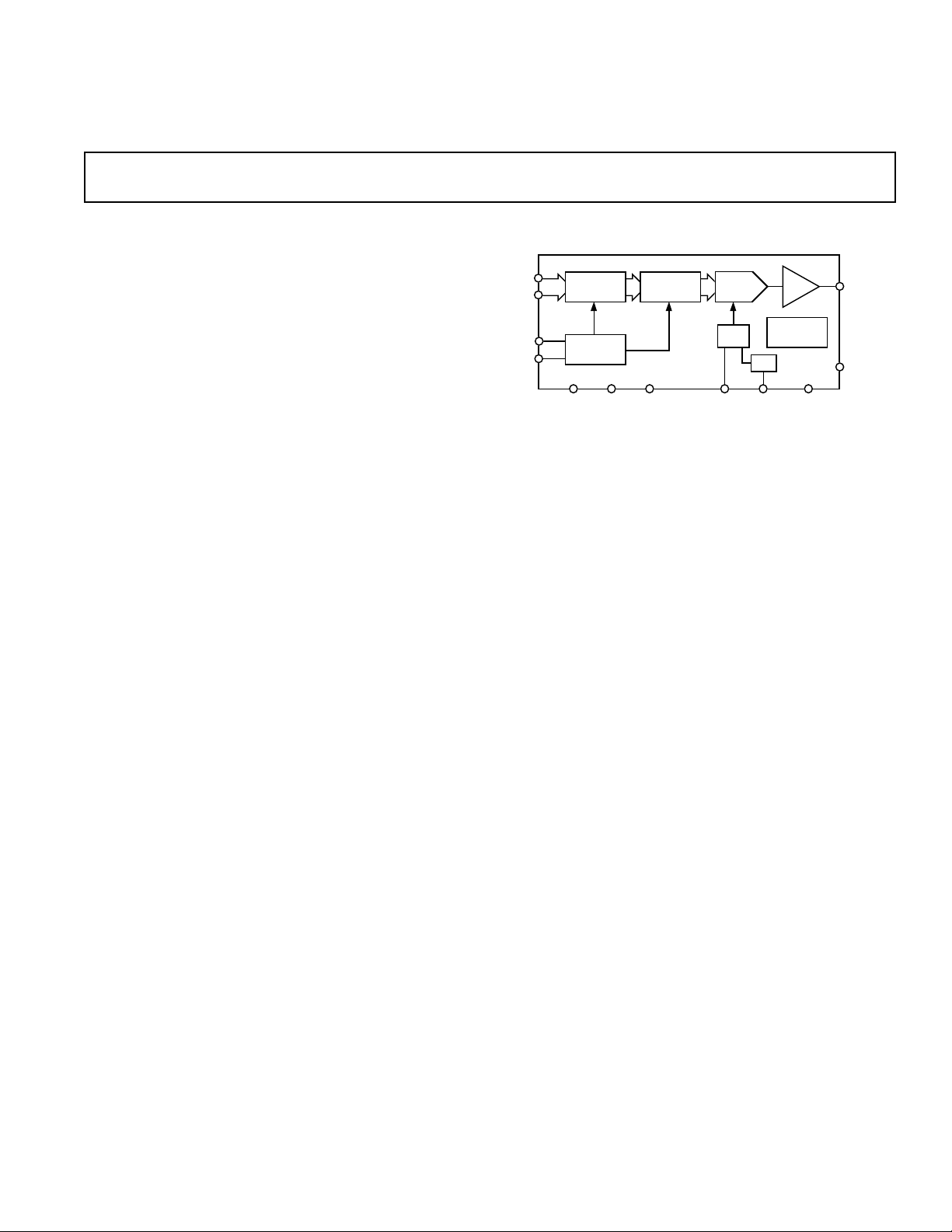
FUNCTIONAL BLOCK DIAGRAM
D7
D0
WR
CS
PRODUCT HIGHLIGHTS
1. Low Power, Single Supply operation. This part operates
from a single +2.7 V to +5.5 V supply and consumes typically
5 mW at 3 V, making it ideal for battery powered applications.
2. The on-chip output buffer amplifier allows the output of the
DAC to swing rail to rail with a settling time of typically 1.2 µs.
3. Internal or external reference capability.
4. High speed parallel interface.
5. Power-down capability. When powered down the DAC
consumes less than 1 µA at 25°C.
6. Packaged in 20-lead SOIC and TSSOP packages.
INPUT
REGISTER
CONTROL
LOGIC
PD CLR LDAC
REGISTER
AD7801
DAC
I DAC
MUX
REFIN V
POWER-ON
RESET
÷
2
DD
I/V
DGND
V
OUT
AGND
REV. 0
Information furnished by Analog Devices is believed to be accurate and
reliable. However, no responsibility is assumed by Analog Devices for its
use, nor for any infringements of patents or other rights of third parties
which may result from its use. No license is granted by implication or
otherwise under any patent or patent rights of Analog Devices.
One Technology Way, P.O. Box 9106, Norwood, MA 02062-9106, U.S.A.
Tel: 617/329-4700 World Wide Web Site: http://www.analog.com
Fax: 617/326-8703 © Analog Devices, Inc., 1997
Page 2
(V
= +2.7 V to +5.5 V, Internal Reference; CL = 100 pF, RL = 10 kV to VDD and GND.
DD
AD7801–SPECIFICA TIONS
All specifications T
Parameter B Versions
1
to T
MIN
unless otherwise noted.)
MAX
Units Conditions/Comments
STATIC PERFORMANCE
Resolution 8 Bits
Relative Accuracy
2
±1 LSB max
Differential Nonlinearity ±1 LSB max Guaranteed Monotonic
Zero-Code Error @ +25°C 3 LSB typ All Zeros Loaded to DAC Register
Full-Scale Error –0.75 LSB typ All Ones Loaded to DAC Register
Zero-Code Error Drift 100 µV/°C typ
Gain Error
3
±1 % FSR typ
DAC REFERENCE INPUT
REFIN Input Range 1 to V
/2 V min/V max
DD
REFIN Input Impedance 10 MΩ typ
OUTPUT CHARACTERISTICS
Output Voltage Range 0 to V
DD
V min/V max
Output Voltage Settling Time 2 µs max Typically 1.2 µs
Slew Rate 7.5 V/µs typ
Digital-to-Analog Glitch Impulse 1 nV-s typ 1 LSB Change Around Major Carry
Digital Feedthrough 0.2 nV-s typ
DC Output Impedance 40 Ω typ
Short Circuit Current 14 mA typ
Power Supply Rejection Ratio
4
0.0003 %/% max ∆VDD = ±10%
LOGIC INPUTS
Input Current ±10 µA max
, Input Low Voltage 0.8 V max VDD = +5 V
V
INL
, Input Low Voltage 0.6 V max VDD = +3 V
V
INL
, Input High Voltage 2.4 V min VDD = +5 V
V
INH
, Input High Voltage 2.1 V min VDD = +3 V
V
INH
Pin Capacitance 7 pF max
POWER REQUIREMENTS
V
DD
(Normal Mode) DAC Active and Excluding Load Current
I
DD
= 3.3 V VIH = VDD and VIL = GND
V
DD
2.7/5.5 V min/V max
@ 25°C 1.55 mA max See Figure 6
T
V
DD
to T
MIN
= 5.5 V
MAX
1.75 mA max
@ 25°C 2.35 mA max
to T
T
MIN
(Power-Down)
I
DD
MAX
@ 25°C1µA max V
T
to T
MIN
NOTES
1
Temperature ranges are as follows: B Version: –40°C to +105 °C
2
Relative Accuracy is calculated using a reduced code range of 15 to 245.
3
Gain Error is specified between Codes 15 and 245. The actual error at Code 15 is typically 3 LSB.
4
Guaranteed by characterization at product release, not production tested.
Specifications subject to change without notice.
MAX
2.5 mA max
= VDD and VIL = GND
IH
2 µA max See Figure 18
CS
WR
D7-D0
LDAC
CLR
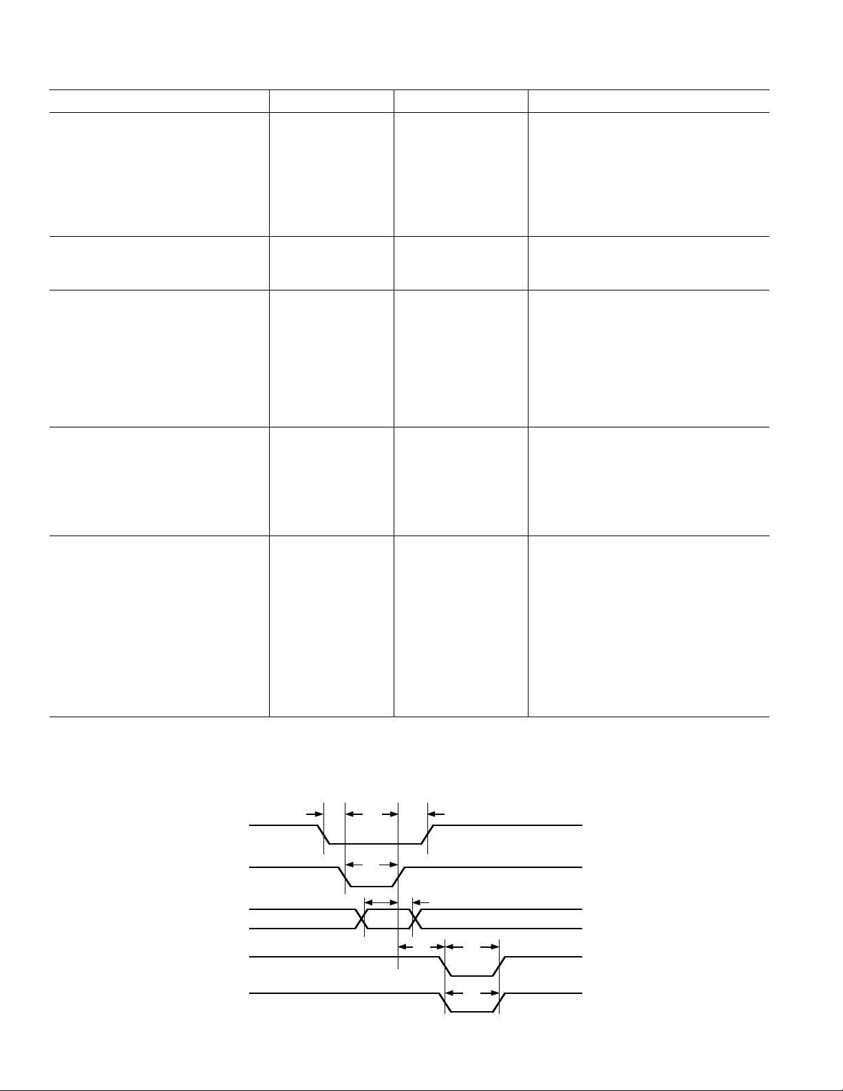
t
1
t
t
2
3
t
t
4
5
t
6
t
7
t
8
Figure 1. Timing Diagram for Parallel Data Write
–2–
REV. 0
Page 3
AD7801
WARNING!
ESD SENSITIVE DEVICE
(VDD = +2.7 V to +5.5 V; GND = 0 V; Internal VDD/2 Reference. All specifications T
TIMING CHARACTERISTICS
Limit at T
1, 2
unless otherwise noted.)
, T
MIN
MAX
Parameter (B Version) Units Conditions/Comments
t
1
t
2
t
3
t
4
t
5
t
6
t
7
t
8
NOTES
1
Sample tested at +25°C to ensure compliance. All input signals are specified with tr = tf = 5 ns (10% to 90% of VDD) and timed from a voltage level of
(VIL + VIH)/2. tr and tf should not exceed 1 µs on any digital input.
2
See Figure 1.
ABSOLUTE MAXIMUM RATINGS*
(TA = +25°C unless otherwise noted)
VDD to GND . . . . . . . . . . . . . . . . . . . . . . . . . . –0.3 V to +7 V
Reference Input Voltage to AGND . . . .–0.3 V to V
Digital Input Voltage to DGND . . . . . .–0.3 V to V
AGND to DGND . . . . . . . . . . . . . . . . . . . . .–0.3 V to +0.3 V
V
to AGND . . . . . . . . . . . . . . . . . . –0.3 V to VDD + 0.3 V
OUT
Operating Temperature Range
0 ns min Chip Select to Write Setup Time
0 ns min Chip Select to Write Hold Time
20 ns min Write Pulse Width
15 ns min Data Setup Time
4.5 ns min Data Hold Time
20 ns min Write to LDAC Setup Time
20 ns min LDAC Pulse Width
20 ns min CLR Pulse Width
ORDERING GUIDE
Temperature Package
+ 0.3 V
DD
+ 0.3 V
DD
Model Range Option*
AD7801BR –40°C to +105°C R-20
AD7801BRU –40°C to +105°C RU-20
*R = Small Outline; RU = Thin Shrink Small Outline.
Commercial (B Version) . . . . . . . . . . . . . –40°C to +105°C
Storage Temperature Range . . . . . . . . . . . . –65°C to +150°C
Junction Temperature . . . . . . . . . . . . . . . . . . . . . . . . .+150°C
SSOP Package, Power Dissipation . . . . . . . . . . . . . . . 700 mW
θ
Thermal Impedance . . . . . . . . . . . . . . . . . . . . 143°C/W
JA
Lead Temperature, Soldering
Vapor Phase (60 sec) . . . . . . . . . . . . . . . . . . . . . . .+215°C
Infrared (15 sec) . . . . . . . . . . . . . . . . . . . . . . . . . .+220°C
SOIC Package, Power Dissipation . . . . . . . . . . . . . . . 870 mW
θ
Thermal Impedance . . . . . . . . . . . . . . . . . . . . . 74°C/W
JA
Lead Temperature, Soldering
Vapor Phase (60 sec) . . . . . . . . . . . . . . . . . . . . . . .+215°C
Infrared (15 sec) . . . . . . . . . . . . . . . . . . . . . . . . . .+220°C
MIN
to T
MAX
*Stresses above those listed under Absolute Maximum Ratings may cause perma-
nent damage to the device. This is a stress rating only; functional operation of the
device at these or any other conditions above those listed in the operational
sections of this specification is not implied. Exposure to absolute maximum rating
conditions for extended periods may affect device reliability.
CAUTION
ESD (electrostatic discharge) sensitive device. Electrostatic charges as high as 4000 V readily
accumulate on the human body and test equipment and can discharge without detection.
Although the AD7801 features proprietary ESD protection circuitry, permanent damage may
occur on devices subjected to high energy electrostatic discharges. Therefore, proper ESD
precautions are recommended to avoid performance degradation or loss of functionality.
REV. 0
–3–
Page 4
AD7801
PIN CONFIGURATION
(MSB) DB7
(LSB) DB0
1
2
DB6
3
DB5
4
DB4
5
AD7801
TOP VIEW
DB2
6
(Not to Scale)
DB1
7
8
9
CS
10
WR DGND
NC = NO CONNECT
20
DGND
19
V
OUT
18
NC
17
AGND
16
REFINDB3
15
V
DD
14
CLR
13
LDAC
12
PD
11
PIN FUNCTION DESCRIPTIONS
Pin
No. Mnemonic Function
1–8 D7–D0 Parallel Data Inputs. 8-bit data is loaded to the input register of the AD7801 under the control of CS and WR.
9 CS Chip Select. Active low logic input.
10 WR Write Input. WR is an active low logic input used in conjunction with CS to write data to the input register.
11 DGND Digital Ground
12 PD Active low input used to put the part into low power mode reducing current consumption to less than 1 µA.
13 LDAC Load DAC Logic Input. When this logic input is taken low the DAC output is updated with the contents of
its DAC register. If LDAC is permanently tied low the DAC is updated on the rising edge of WR.
14 CLR Asynchronous Clear Input (Active Low). When this input is taken low the DAC register is loaded with all
zeroes and the DAC output is cleared to zero volts.
15 V
DD
Power Supply Input. This part can be operated from +2.7 V to +5.5 V and should be decoupled to GND.
16 REFIN External Reference Input. This can be used as the reference for the DAC. The range on this reference input is
1 V to V
/2. If REFIN is tied directly to VDD the internal VDD/2 reference is selected.
DD
17 AGND Analog Ground reference point and return point for all analog current on the part.
18 NC No Connect Pin.
19 V
OUT
Analog Output Voltage from the DAC. The output amplifier can swing rail to rail on its output.
20 DGND Digital Ground reference point and return point for all digital current on the part.
–4–
REV. 0
Page 5
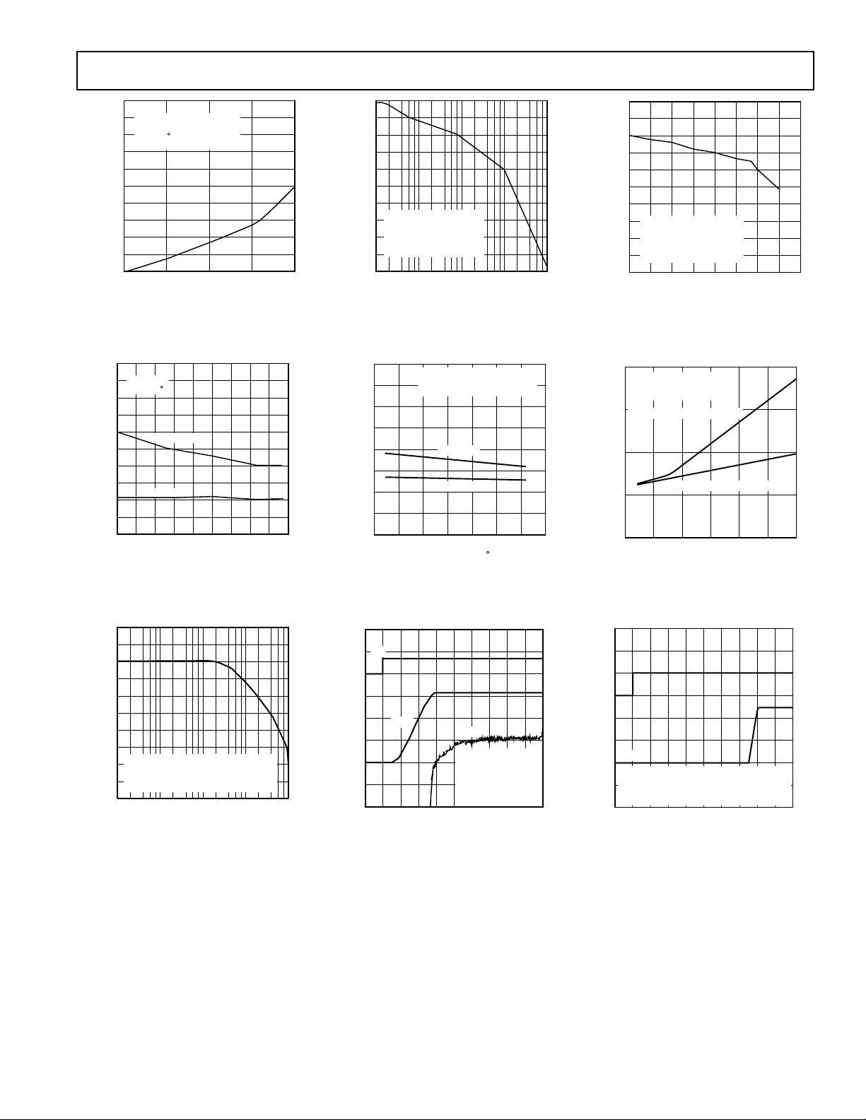
Typical Performance Characteristics–
5
800
VDD = 5V AND 3V
720
INTERNAL REFERENCE
640
T
= +25 C
A
DAC LOADED WITH 00HEX
560
480
400
– mV
OUT
320
V
240
160
80
0
08
24 6
SINK CURRENT – mA
4.92
4.84
4.76
4.68
4.6
Volts
–
4.52
OUT
V
= 5V
DD
V
4.44
INTERNAL REFERENCE
DAC REGISTER LOADED
4.36
WITH FFHEX
T
= +25°C
A
4.28
4.2
02 846
SOURCE CURRENT – mA
AD7801
3.5
3.25
3.0
2.75
2.5
2.25
– Volts
2.0
OUT
V
VDD = 3V
1.75
INTERNAL REFERENCE
DAC REGISTER LOADED
1.5
WITH FFHex
1.25
T
= +25°C
A
1.0
01 8234567
SOURCE CURRENT – mA
Figure 2. Output Sink Current Capability with V
0.5
0.45
0.4
0.35
0.3
0.25
0.2
ERROR – LSBs
0.15
0.1
0.05
0
1.0 1.2 2.8
= 3 V and VDD = 5 V
DD
VDD = 5V
= +25 C
T
A
INL ERROR
DNL ERROR
1.4 1.6 1.8 2.2 2.4 2.62.0
REFERENCE VOLTAGE – Volts
Figure 5. Relative Accuracy vs.
External Reference
10
5
0
–5
–10
–15
–20
–25
ATTENUATION – dB
VDD = 5V
–30
EXTERNAL SINEWAVE REFERENCE
DAC REGISTER LOADED WITH FFHEX
–35
T
= +25°C
A
–40
1 10 10k100 1k
FREQUENCY – Hz
Figure 8. Large Scale Signal
Frequency Response
Figure 3. Output Source Current
Capability with V
4.0
3.5
3.0
2.5
2.0
– mA
DD
I
1.5
1.0
0.5
0
–50 –25
INTERNAL REFERENCE
LOGIC INPUTS = V
DAC ACTIVE
TEMPERATURE – C
= 5 V
DD
OR GND
DD
VDD = 5.5V
VDD = 3.3V
0 255075 125
100
Figure 6. Typical Supply Current
vs. Temperature
WR
T
1
←
←
2
V
OUT
3
←
CH1 5V, CH2 1V, CH3 20mV
TIME BASE = 200 ns/Div
V
OUT
VDD = 3V
INTERNAL VOLTAGE
REFERENCE
FULL SCALE CODE
CHANGE 00H-FFH
T
= +25°C
A
←
Figure 9. Full-Scale Settling Time
Figure 4. Output Source Current
Capability with V
4.0
DAC ACTIVE
INTERNAL REFERENCE
T
= +25°C
A
3.0
LOGIC INPUTS = VIH OR V
2.0
– mA
DD
I
1.0
0
2.5 3.0 5.53.5 4.0 4.5 5.0
LOGIC INPUTS = V
= 3 V
DD
VDD – Volts
IL
OR GND
DD
Figure 7. Typical Supply Current
vs. Supply Voltage
PD
2
←
V
OUT
←
1
AD7801 POWER-UP TIME
= 5V
V
DD
INTERNAL REFERENCE
DAC IN POWER-DOWN INITIALLY
CH1 = 2V/div, CH2 = 5V/Div,
TIME BASE = 2 µs/Div
Figure 10. Exiting Power-Down (Full
Power-Down)
REV. 0
–5–
Page 6

AD7801
1
2
–Typical Performance Characteristics
T
T
V
CH1
5.00V CH2 5.00V CH1
Figure 11. Power-On—Reset
OUT
V
DD
M20.0ms
10
9
8
7
VDD = 2.7 TO 5.5V
6
DAC LOADED WITH ALL ZEROES
INTERNAL REFERENCE
5
4
3
2
ZERO CODE ERROR – LSB
1
0
–50 0 25 50 75 100 125
–25
TEMPERATURE – C
Figure 12. Zero Code Error vs.
Temperature
WR
1
←
V
OUT
2
←
CH1 5.00V, CH2 50.0mV, M 250ns
VDD = 5V
INTERNAL VOLTAGE
REFERENCE
10 LSB STEP CHANGE
T
= +258C
A
Figure 13. Small-Scale Settling Time
0.5
VDD = 5V
0.4
INTERNAL REFERENCE
5kΩ 100pF LOAD
0.3
LIMITED CODE RANGE (15–245)
T
= +25°C
A
0.2
0.1
0
–0.1
INL ERROR – LSB
–0.2
–0.3
–0.4
–0.5
0 25632 64 96 128 160 192 224
INPUT CODE (15 to 245)
Figure 14. Integral Linearity Plot
1.0
V
= 5V
DD
0.8
0.6
0.4
0.2
INT REFERENCE ERROR – %
0
–60 –40 –20 0 20 40 60 80 100 120 140
Figure 17. Typical Internal Reference
Error vs. Temperature
0.5
0.4
0.3
0.2
V
= 5V
DD
INTERNAL REFERENCE
0.1
0
–0.1
INL ERROR – LSB
–0.2
–0.3
–0.4
–0.5
–60 –40 –20 0 20 40 60 80 100 120 140
TEMPERATURE – C
Figure 15. Typical INL vs. Temperature
TEMPERATURE –
C
Figure 18. Power-Down Current vs.
Temperature
Figure 16. Typical DNL vs. Temperature
1000
900
800
700
600
500
400
300
200
POWER DOWN CURRENT – nA
100
0
–50 –25
VDD = 5V
LOGIC INPUTS = VDD OR GND
0255075100
TEMPERATURE – C
0.5
0.4
0.3
0.2
V
0.1
–0.1
DNL ERROR – LSB
–0.2
–0.3
–0.4
–0.5
= 5V
DD
INTERNAL REFERENCE
0
–60 –40 –20 0 20 40 60 80 100 120 140
TEMPERATURE –
150
C
–6–
REV. 0
Page 7

TERMINOLOGY
Integral Nonlinearity
For the DAC, Relative Accuracy or End-Point nonlinearity is a
measure of the maximum deviation, in LSBs, from a straight
line passing through the endpoints of the DAC transfer
function. A graphical representation of the transfer curve is
shown in Figure 14.
Differential Nonlinearity
Differential Nonlinearity is the difference between the measured change and the ideal 1 LSB change between any two
adjacent codes. A specified differential nonlinearity of ± 1 LSB
maximum ensures monotonicity.
Zero-Code Error
Zero-Code Error is the measured output voltage from V
OUT
of
the DAC when zero code (all zeros) is loaded to the DAC
latch. It is due to a combination of the offset errors in the DAC
and output amplifier. Zero-code error is expressed in LSBs.
Gain Error
This is a measure of the span error of the DAC. It is the
deviation in slope of the DAC transfer characteristic from ideal
expressed as a percent of the full-scale value. It includes fullscale errors but not offset errors.
Digital-to-Analog Glitch Impulse
Digital-to-Analog Glitch Impulse is the impulse injected into
the analog output when the digital inputs change state with
the DAC selected and the LDAC used to update the DAC. It
is normally specified as the area of the glitch in nV-secs and
measured when the digital input code is changed by 1 LSB at
the major carry transition.
Digital Feedthrough
Digital Feedthrough is a measure of the impulse injected into
the analog output of a DAC from the digital inputs of the same
DAC, but is measured when the DAC is not updated. It is
specified in nV-secs and measured with a full-scale code change
on the data bus, i.e., from all 0s to all 1s and vice versa.
Power Supply Rejection Ratio (PSRR)
This specification indicates how the output of the DAC is affected
by changes in the power supply voltage. Power supply rejection
ratio is quoted in terms of % change in output per % change in
V
for full-scale output of the DAC. VDD is varied ±10%.
DD
GENERAL DESCRIPTION
D/A Section
The AD7801 is an 8-bit voltage output digital-to-analog converter. The architecture consists of a reference amplifier and a
current source DAC followed by a current-to-voltage converter
capable of generating rail-to-rail voltages on the output of the
DAC. Figure 19 shows a block diagram of the basic DAC
architecture.
AD7801
PMOS
INT
REF
AD7801
11.7kΩ
CURRENT
DAC
11.7kΩ
and ground. The
DD
/2 V. The output voltage
DD
N
×
REF
256
VTH
COMPARATOR
MUX
SELECTED REFERENCE
OUTPUT
I/V
V
OUT
REFERENCE
AMPLIFIER
REFIN
V
DD
30kΩ
30kΩ
Figure 19. DAC Architecture
The DAC output is internally buffered and has rail-to-rail
output characteristics. The output amplifier is capable of driving
a load of 100 pF and 10 kΩ to both V
reference selection for the DAC can be either internally generated from V
or externally applied through the REFIN pin. A
DD
comparator on the REFIN pin detects whether the required
reference is the internally generated reference or the externally
applied voltage to the REFIN pin. If REFIN is connected to
V
, the reference selected is the internally generated VDD/2
DD
reference. When an externally applied voltage is more than one
volt below V
, the comparator selection switches to the externally
DD
applied voltage on the REFIN pin. The range on the external
reference input is from 1.0 V to V
from the DAC is given by:
VO=2V
where V
V
DD
is the voltage applied to the external REFIN pin or
REF
/2 when the internal reference is selected. N is the decimal
equivalent of the code loaded to the DAC register and ranges
from 0 to 255.
V
DD
INT REF
EXT REF
REF
IN
Figure 20. Reference Selection Circuitry
REV. 0
–7–
Page 8

AD7801
Reference
The AD7801 has the ability to use either an external reference
applied through the REFIN pin or an internal reference generated
from V
where either the internal V
. Figure 20 shows the reference input arrangement
DD
/2 or the externally applied reference
DD
can be selected.
The internal reference is selected by tying the REFIN pin to
V
. If an external reference is to be used, this can be directly
DD
applied to the REFIN pin and if this is 1 V below V
DD
, the
internal circuitry will select this externally applied reference as
the reference source for the DAC.
Digital Interface
The AD7801 contains a fast parallel interface allowing this
DAC to interface to industry standard microprocessors,
microcontrollers and DSP machines. There are two modes in
which this parallel interface can be configured to update the
DAC output. The synchronous update mode allows synchronous updating of the DAC output; the automatic update mode
allows the DAC to be updated individually following a write
cycle. Figure 21 shows the internal logic associated with the
digital interface. The PON STRB signal is internally generated
from the power-on reset circuitry and is low during the poweron reset phase of the power up procedure.
CLR
CLR
PON STRB
MLE
SLE
LDAC
CS
WR
CLEAR
SET SLE
LDAC
ENABLE
DAC CONTROL
LOGIC
Figure 21. Logic Interface
The AD7801 has a double buffered interface, which allows for
synchronous updating of the DAC output. Figure 22 shows a
block diagram of the register arrangement within the AD7801.
Automatic Update Mode
In this mode of operation the LDAC signal is permanently tied
low. The state of the LDAC is sampled on the rising edge of
WR. LDAC being low allows the DAC register to be automatically updated on the rising edge of WR. The output update
occurs on the rising edge of WR. Figure 23 shows the timing
associated with the automatic update mode of operation and
also the status of the various registers during this frame.
CS
WR
D7-D0
LDAC = 0
I/P REG (MLE)
DAC REG (SLE)
V
OUT
HOLD HOLD
TRACK TRACK
TRACK
HOLD
Figure 23. Timing and Register Arrangement for Automatic Update Mode
Synchronous Update Mode
In this mode of operation the LDAC signal is used to update the
DAC output to synchronize with other updates in the system.
The state of the LDAC is sampled on the rising edge of WR. If
LDAC is high, the automatic update mode is disabled and the
DAC latch is updated at any time after the write by taking
LDAC low. The output update occurs on the falling edge of
LDAC. LDAC must be taken back high again before the next
data transfer takes place. Figure 24 shows the timing associated
with the synchronous update mode of operation and also the
status of the various registers during this frame.
CS
DB7-DB0
CS
WR
LDAC
CLR
INPUT
REGISTER
4
8
4
MLE SLE
CONTROL LOGIC
15 15 30
4 TO 15
DECODER
4 TO 15
DECODER
DAC
REGISTER
15 15 30
DAC
REGISTER
Figure 22. Register Arrangement
UPPER
DRIVERS
NIBBLE
DRIVERS
LOWER
NIBBLE
WR
D7-D0
LDAC
I/P REG (MLE)
DAC REG (SLE)
V
OUT
HOLD HOLD
TRACK
HOLD HOLDTRACK
Figure 24. Timing and Register Arrangement for Synchronous Update Mode
–8–
REV. 0
Page 9

AD7801
POWER-ON RESET
The AD7801 has a power-on reset circuit designed to allow
output stability during power up. This circuit holds the DAC in
a reset state until a write takes place to the DAC. In the reset
state all zeros are latched into the input register of the DAC and
the DAC register is in transparent mode thus the output of the
DAC is held at ground potential until a write takes place to the
DAC. The power-on reset circuitry generates a PON STRB
signal which is a gating signal used within the logic to identify
a power-on condition.
POWER-DOWN FEATURES
The AD7801 has a power-down feature implemented by
exercising the external PD pin. An active low signal puts the
complete DAC into power-down mode. When in power-down,
the current consumption of the device is reduced to less than
1 µA max at +25°C or 2 µA max over temperature, making the
device suitable for use in portable battery powered equipment.
The internal reference resistors, the reference bias servo loop,
the output amplifier and associated linear circuitry are all shut
down when the power-down is activated. The output terminal
sees a load of ≈ 23 kΩ to GND when in power-down mode as
shown in Figure 25. The contents of the data register are
unaffected when in power-down mode. The device typically
comes out of power-down in 13 µs (see Figure 10).
11.7kΩ
V
DD
I
DAC
V
=2×V
O
UT
REF
N
256
where:
N is the decimal equivalent of the binary input
code. N ranges from 0 to 255.
V
is the voltage applied to the external REFIN pin
REF
when the external reference is selected and is V
if the internal reference is used.
Table I. Output Voltage for Selected Input Codes
Digital Analog Output
MSB . . . LSB
255
2×
×V
×V
×V
×V
V
REF
V
REF
V
REF
V
REF
V
1111 1111
1111 1110
1000 0001
1000 0000 V
0111 1111
0000 0001
2×
2×
2×
2×
REF
256
254
256
129
256
V
127
256
V
256
REF
0000 0000 0 V
DD
/2
11.7kΩ
V
REF
Figure 25. Output Stage During Power-Down
Analog Outputs
The AD7801 contains a voltage output DAC with 8-bit resolution
and rail-to-rail operation. The output buffer provides a gain of
two at the output. Figures 2, 3 and 4 show the source and sink
capabilities of the output amplifier. The slew rate of the output
amplifier is typically 7.5 V/µs and has a full-scale settling to
eight bits with a 100 pF capacitive load in typically 1.2 µs.
The input coding to the DAC is straight binary. Table I shows
the binary transfer function for the AD7801. Figure 26 shows
the DAC transfer function for binary coding. Any DAC output
voltage can be expressed as:
2V
REF
V
REF
DAC OUTPUT VOLTAGE
0
DAC INPUT CODE 00 01 7F 80 81 FE FF
Figure 26. DAC Transfer Function
REV. 0
–9–
Page 10

AD7801
Figure 27 shows a typical setup for the AD7801 when using its
internal reference. The internal reference is selected by tying the
REFIN pin to V
reference detect circuit that will select the internal V
. Internally in the reference section there is a
DD
/2 based
DD
on the voltage connected to the REFIN pin. If REFIN is within
a threshold voltage of a PMOS device (approximately 1 V) of
V
the internal reference is selected. When the REFIN voltage
DD
is more than 1 V below V
, the externally applied voltage at
DD
this pin is used as the reference for the DAC. The internal
reference on the AD7801 is V
/2, the output current to
DD
voltage converter within the AD7801 provides a gain of two.
Thus the output range of the DAC is from 0 V to V
, based on
DD
Table I.
VDD = 3V TO 5V
10mF0.1mF
AGND DGND
V
D7-D0
DD
AD7801
CS WR LDAC
INPUTS
V
OUT
V
OUT
REF IN
CLR
PD
V
DD
DATA BUS CONTROL
Figure 27. Typical Configuration Selecting the Internal
Reference
Figure 28 shows a typical setup for the AD7801 when using an
external reference. The reference range for the AD7801 is from
1 V to VDD/2 V. Higher values of reference can be incorporated
but will saturate the output at both the top and bottom end of
the transfer function. There is a gain of two from input to output
on the AD7801. Suitable references for 5 V operation are the
AD780 and REF192. For 3 V operation a suitable external
reference would be the AD589 a 1.23 V bandgap reference.
VDD = 3V TO 5V
10mF0.1mF
V
IN
EXT REF
AD780/REF192 WITH V
AD589 WITH V
GND
OR
V
DD
OUT
DD
= 3V
= 5V
0.1mF
V
DD
V
AGND DGND
D7-D0
DD
AD7801
CS
INPUTS
WR
REF IN
CLR
PD
DATA BUS CONTROL
V
LDAC
OUT
V
OUT
Figure 28. Typical Configuration Using An External
Reference
MICROPROCESSOR INTERFACING
AD7801–ADSP-2101/ADSP-2103 Interface
Figure 29 shows an interface between the AD7801 and the ADSP2101/ADSP-2103. The fast interface timing associated with the
AD7801 allows easy interface to the ADSP-2101/ADSP-2103.
LDAC is permanently tied low in this circuit so the DAC
output is updated on the rising edge of the WR signal.
Data is loaded to the AD7801 input register using the following
ADSP-21xx instruction.
DM(DAC) = MR0
MR0 = ADSP-21xx MR0 Register.
DAC = Decoded DAC Address.
DMA14
DMA0
DMS
ADSP-2101*/
ADSP-2103*
WR
DMD15
DMD0
*
ADDRESS BUS
ADDR
EN
DECODE
DATA BUS
ADDITIONAL CIRCUITRY OMITTED FOR CLARITY.
AD7801*
CS
LDAC
WR
DB7
DB0
Figure 29. AD7801–ADSP-2101/ADSP-2103 Interface
AD7801–TMS320C20 Interface
Figure 30 shows an interface between the AD7801 and the
TMS320C20. Data is loaded to the AD7801 using the following
instruction:
OUT DAC, D
DAC = Decoded DAC Address.
D = Data Memory Address.
A15
A0
IS
TMS320C20
STRB
R/W
D15
D0
*
ADDRESS BUS
ADDR
EN
DECODE
DATA BUS
ADDITIONAL CIRCUITRY OMITTED FOR CLARITY.
AD7801*
CS
LDAC
WR
DB7
DB0
–10–
Figure 30. AD7801–TMS320C20 Interface
REV. 0
Page 11

AD7801
In the circuit shown the LDAC is hardwired low thus the DAC
output is updated on the rising edge of WR. Some applications
may require synchronous updating of the DAC in the AD7801.
In this case the LDAC signal can be driven from an external
timer or can be controlled by the microprocessor. One option
for synchronous updating is to decode the LDAC from the address bus so a write operation at this address will synchronously
update the DAC output. A simple OR gate with one input
driven from the decoded address and the second input from the
WR signal will implement this function.
AD7801–8051/8088 Interface
Figure 31 shows a serial interface between the AD7801 and the
8051/8088 processors.
PSEN OR DEN
8051/8088*
A15
A8
WR
ALE
AD7
AD0
OCTAL
LATCH
*
ADDRESS BUS
ADDR
EN
DECODE
DATA BUS
ADDITIONAL CIRCUITRY OMITTED FOR CLARITY.
AD7801*
CS
WR
LDAC
DB7
DB0
V
IN
EXT REF
GND
AD780/REF192
WITH V
DD
OR
AD589 WITH V
V
= 5V
DD
OUT
= 3V
0.1mF
V
DD
10mF0.1mF
REF IN
CLR
PD
D7-D0
DATA
BUS
VDD = 3V TO 5V
AGND DGND
V
DD
AD7801
CS
WR LDAC
CONTROL
INPUTS
R3
10kΩ
V
OUT
R1
10kΩ
R2
20kΩ
R4
20kΩ
AD820/
OP295
+5V
±5V
–5V
Figure 32. Bipolar Operation Using the AD7801
Decoding Multiple AD7801s in a System
The CS pin on the AD7801 can be used in applications to
decode a number of DACs. In this application, all DACs in the
system receive the same input data, but only the CS to one of
the DACs will be active at any one time allowing access to one
channel in the system. The 74HC139 is used as a two-to-four
line decoder to address any of the DACs in the system. To
prevent timing errors from occurring, the Enable input on the
74HC139 should be brought to its inactive state while the
Coded Address inputs are changing state. Figure 33 shows a
diagram of a typical setup for decoding multiple AD7801
devices in a system. The built-in power-on reset circuit on the
AD7801 ensures that the outputs of all DACs in the system
power up with zero volts on their outputs.
Figure 31. AD7801–8051/8088 Interface
APPLICATIONS
Bipolar Operation Using the AD7801
The AD7801 has been designed for unipolar operation but
bipolar operation is possible using the circuit in Figure 32. The
circuit shown is configured for an output voltage range of –5 V
to +5 V. Rail-to-rail operation at the amplifier output is achievable
by using an AD820 or OP295 as the output amplifier.
The output voltage for any input code can be calculated as
follows:
VO= R21+
R4
/ R1+R2
()
R3
2V
REF
×
256
D
−V
REF
R4
R3
Where D is the decimal equivalent of the code loaded to the
DAC and V
With V
REF
V
= 5 V.
DD
is the reference voltage input.
REF
= 2.5 V, R1 = R3 = 10 kΩ and R2 = R4 = 20 kΩ and
10D
VO=
256
–5
DATA BUS
WR
ENABLE
CODED
ADDRESS
V
DD
V
CC
1G
1A
1B
74HC139
DGND
1Y0
1Y1
1Y2
1Y3
AD7801
CS
WR
D0
D7
AD7801
CS
WR
D0
D7
AD7801
CS
WR
D0
D7
AD7801
CS
WR
D0
D7
Figure 33. Decoding Multiple AD7801s
LDAC
LDAC
LDAC
LDAC
V
OUT
V
OUT
V
OUT
V
OUT
REV. 0
–11–
Page 12

AD7801
AD7801
V
OUT
REF IN
VDD = 5V
V
DD
AGND DGND
10µF0.1µF
0.1µF
EXT REF
V
OUT
V
IN
GND
AD780/ REF192
WITH V
DD
= 5V
OR
AD589 WITH V
DD
= 3V
+5V
AD820/
OP295
R1
390Ω
AD7801
V
OUT
REF IN
V
DD
AGND DGND
R2
51.2kΩ
V
O
R3
51.2kΩ
R4
390Ω
0.1µF
AD7801 as a Digitally Programmable Indicator
A digitally programmable upper limit detector using the DAC is
shown in Figure 34. The upper limit for the test is loaded to the
DAC, which in turn sets the limit for the CMP04. If a signal at
the V
input is not below the programmed value, an LED will
IN
indicate the Fail condition.
+5V
0.1
F
10 F
VDDREFIN
V
IN
1kΩ
FAIL
1kΩ
PASS
AD7801
V
OUT
DV
D7
D0
1/4
DD
DGND AGND
CMP-04
PASS/
1/6
74HC05
Figure 34. Digitally Programmable Indicator
Programmable Current Source
Figure 35 shows the AD7801 used as the control element of a
programmable current source. In this circuit the full-scale
current is set to 1 mA. The output voltage from the DAC is
applied across the current setting resistor of 4.7 kΩ in series with
the full-scale setting resistor of 470 Ω. Suitable transistors to
place in the feedback loop of the amplifier include the BC107
and the 2N3904, which enable the current source to operate
from a minimum V
of 6 V. The operating range is
SOURCE
determined by the operating characteristics of the transistor.
Suitable amplifiers include the AD820 and the OP295, both of
which have rail-to-rail operation on their outputs. The current
for any digital input code can be calculated as follows:
VDD = 5V
V
V
IN
EXT REF
AD780/ REF192
WITH V
GND
V
= 5V
DD
OUT
0.1µF
10µF0.1µF
REF IN
V
DD
AD7801
AGND DGND
V
OUT
AD820/
OP295
+5V
LOAD
SOURCE
4.7kΩ
2N3904/
BC107
470Ω
Figure 35. Programmable Current Source
Coarse and Fine Adjustment using two AD7801s
The two DACs can be paired together to form a coarse and fine
adjustment function for a setpoint as shown in Figure 36. In this
circuit, the first DAC is used to provide the coarse adjustment
and the second DAC is used to provide the fine adjustment.
Varying the ratio of R1 and R2 will vary the relative effect of the
coarse and fine tune elements in the circuit. For the resistor
values shown, the second DAC has a resolution of 148 µV
giving a fine tune range of 38 mV (approximately 2 LSB) for
operation with a V
of 5 V and a reference of 2.5 V. The
DD
amplifier shown allows a rail-to-rail output voltage to be
achieved on the output. A typical application for the circuit
would be in a setpoint controller.
I =
D
2V
()
REF
256 (5 kΩ)
()
–12–
Figure 36. Coarse and Fine Adjustment
REV. 0
Page 13

AD7801
Power Supply Bypassing and Grounding
In any circuit where accuracy is important, careful consideration
of the power supply and ground return layout helps to ensure
the rated performance. The printed circuit board on which the
AD7801 is mounted should be designed so that the analog and
digital sections are separated and confined to certain areas of the
board. If the AD7801 is in a system where multiple devices
require an AGND to DGND connection, the connection should
be made at one point only, a star ground point which should be
established as closely as possible to the AD7801. The AD7801
should have ample supply bypassing of 10 µF in parallel with
0.1 µF located as close to the package as possible, ideally right
up against the device. The 10 µF capacitors are the tantalum
bead type. The 0.1 µF capacitors should have low Effective
Series Resistance (ESR) and Effective Series Inductance (ESI),
such as the common ceramic types, which provide a low
impedance path to ground at high frequencies to handle
transient currents due to internal logic switching.
The power supply lines of the AD7801 should use as large a
trace as possible to provide low impedance paths and reduce the
effects of glitches on the supply line. Fast switching signals like
clocks should be shielded with digital ground to avoid radiating
noise to other parts of the board and should never be run near
reference inputs. Avoid crossover of digital and analog signals.
Traces on opposite sides of the board should run at right angles
to each other. This reduces the effect of feedthrough through
the board. A microstrip technique is by far the best, but not
always possible with a double-sided board. In this technique, the
component side of the board is dedicated to the ground plane
while signal traces are placed on the solder side.
REV. 0
–13–
Page 14

AD7801
OUTLINE DIMENSIONS
Dimensions shown in inches and (mm).
20-Lead Wide Body SOIC
(R-20)
0.5118 (13.00)
0.4961 (12.60)
20 11
0.2992 (7.60)
0.2914 (7.40)
101
0.4193 (10.65)
0.3937 (10.00)
0.0118 (0.30)
0.0040 (0.10)
0.177 (4.50)
0.006 (0.15)
0.002 (0.05)
SEATING
PLANE
PIN 1
0.0500
0.0192 (0.49)
(1.27)
0.0138 (0.35)
BSC
0.260 (6.60)
0.252 (6.40)
20 11
0.169 (4.30)
1
PIN 1
0.0256 (0.65)
BSC
0.1043 (2.65)
0.0926 (2.35)
SEATING
0.0125 (0.32)
PLANE
0.0091 (0.23)
20-Lead TSSOP
(RU-20)
0.256 (6.50)
0.246 (6.25)
10
0.0433
(1.10)
0.0118 (0.30)
0.0075 (0.19)
MAX
0.0079 (0.20)
0.0035 (0.090)
0.0291 (0.74)
0.0098 (0.25)
8°
0°
8°
0°
x 45°
0.0500 (1.27)
0.0157 (0.40)
0.028 (0.70)
0.020 (0.50)
–14–
REV. 0
Page 15

–15–
Page 16

C2995–12–4/97
–16–
PRINTED IN U.S.A.
 Loading...