

Page 1
24-Bit, 312 kSPS, 109 dB Σ-Δ ADC
V
A–V
V
VIN–
www.BDTIC.com/ADI
with On-Chip Buffers and Serial Interface
FEATURES
High performance 24-bit ∑-∆ ADC
115 dB dynamic range at 78 kHz output data rate
109 dB dynamic range at 312 kHz output data rate
312 kHz maximum fully filtered output word rate
Pin-selectable oversampling rate (64×, 128×, and 256×)
Low power mode
Flexible SPI
Fully differential modulator input
On-chip differential amplifier for signal buffering
On-chip reference buffer
Full band low-pass finite impulse response (FIR) filter
Overrange alert pin
Digital gain correction registers
Power-down mode
Synchronization of multiple devices via
Daisy chaining
APPLICATIONS
Data acquisition systems
Vibration analysis
Instrumentation
GENERAL DESCRIPTION
The AD7764 is a high performance, 24-bit Σ- analog-to-digital
converter (ADC). It combines wide input bandwidth, high
speed, and performance of 109 dB dynamic range at a 312 kHz
output data rate. With excellent dc specifications, the converter
is ideal for high speed data acquisition of ac signals where dc
data is also required.
Using the AD7764 eases the front-end antialias filtering
equirements, simplifying the design process significantly. The
r
AD7764 offers pin-selectable decimation rates of 64×, 128×,
and 256×. Other features include an integrated buffer to drive
the reference as well as a fully differential amplifier to buffer
and level shift the input to the modulator.
An overrange alert pin indicates when an input signal has
exce
eded the acceptable range. The addition of internal gain
and internal overrange registers make the AD7764 a compact,
highly integrated data acquisition device requiring minimal
peripheral components.
The AD7764 also offers a low power mode, significantly
educing power dissipation without reducing the output data
r
rate or available input bandwidth.
SYNC
pin
AD7764
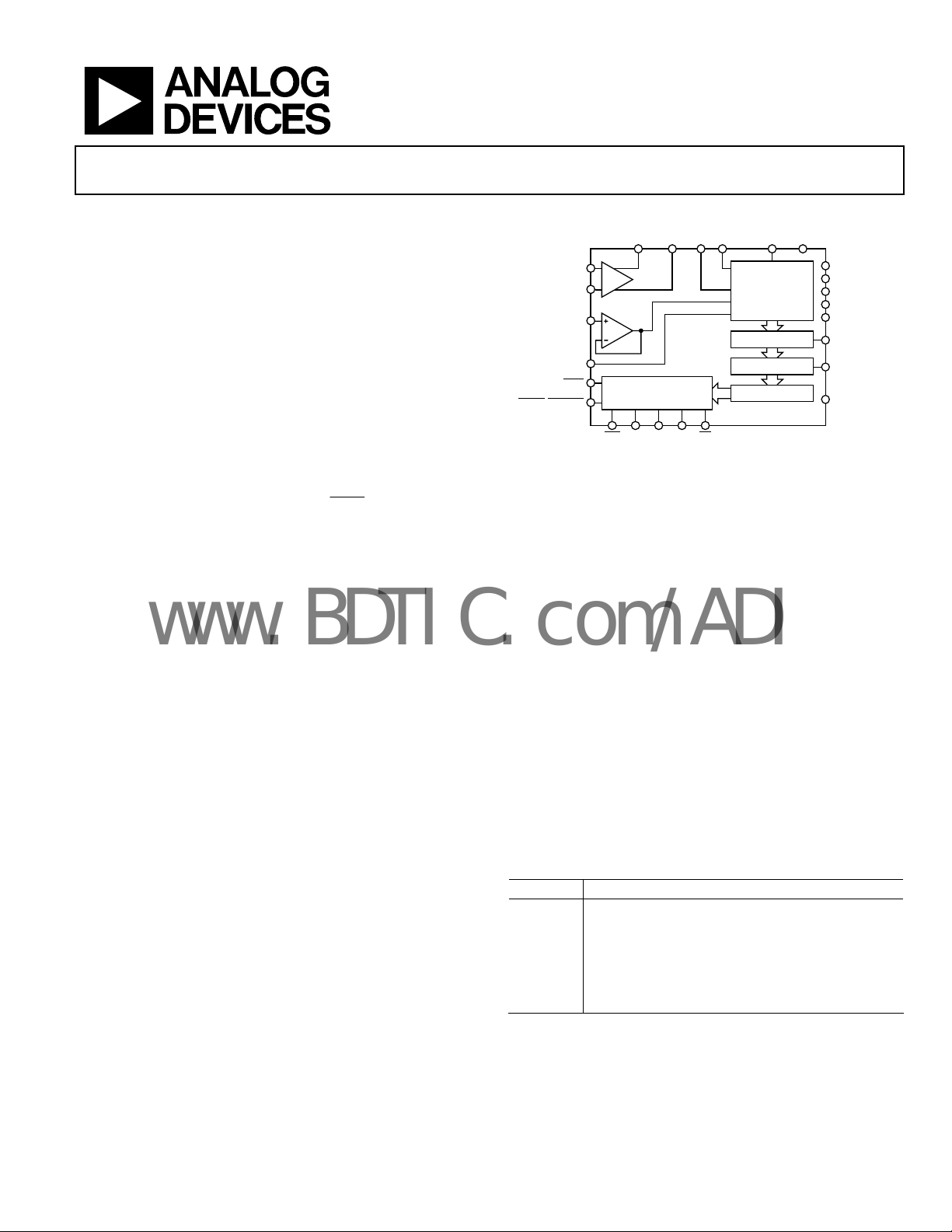
FUNCTIONAL BLOCK DIAGRAM
OUT
VINA+
DIFF
V
A–
IN
V
+
REF
BUF
REFGND
SYNC
RESET/PWRDWN
The differential input is sampled at up to 40 MSPS by an analog
modulator. The modulator output is processed by a series of
low-pass filters. The external clock frequency applied to the
AD7764 determines the sample rate, filter corner frequencies,
and output word rate.
The AD7764 device boasts a full band on-board FIR filter. The
ull stop-band attenuation of the filter is achieved at the Nyquist
f
frequency. This feature offers increased protection from signals
that lie above the Nyquist frequency being aliased back into the
input signal bandwidth.
The reference voltage supplied to the AD7764 determines the
i
nput range. With a 4 V reference, the analog input range is
±3.2768 V differential biased around a common mode of
2.048 V. This common-mode biasing can be achieved using
the on-chip differential amplifier, further reducing the external
signal conditioning requirements.
The AD7764 is available in a 28-lead TSSOP package and is
s
pecified over the industrial temperature range from −40°C
to +85°C.
Tabl e 1. Re l ate d D ev ice s
Part No. Description
AD7760 2.5 MSPS, 100 dB, parallel output on-chip buffers
AD7762 625 kSPS, 109 dB, parallel output on-chip buffers
AD7763 625 kSPS, 109 dB, serial output, on-chip buffers
AD7765 156 kSPS, 112 dB, serial output, on-chip buffers
AD7766 125 kSPS, 108 dB, serial output, 20 mW max power
AD7767 125 kSPS, 108 dB, serial output, 20 mW max Power
INTERFACE LOG IC AND
OFFSET AND GAIN
CORRECTION REGISTERS
FSO SCO SDI SDO FSI
OUT
A+
IN
Figure 1.
+
RECONSTRUCTION
FIR FILTER ENGINE
MULTIBIT
Σ-Δ
MODULATOR
DECIMATION
AD7764
GNDMCLK
AVDD1
AVDD2
AVDD3
AVDD4
DV
DD
OVERRANGE
DEC_RATE
R
BIAS
06518-001
Rev. 0
Information furnished by Analog Devices is believed to be accurate and reliable. However, no
responsibility is assumed by Anal og Devices for its use, nor for any infringements of patents or ot her
rights of third parties that may result from its use. Specifications subject to change without notice. No
license is granted by implication or otherwise under any patent or patent rights of Analog Devices.
Trademarks and registered trademarks are the property of their respective owners.
One Technology Way, P.O. Box 9106, Norwood, MA 02062-9106, U.S.A.
Tel: 781.329.4700 www.analog.com
Fax: 781.461.3113 ©2007 Analog Devices, Inc. All rights reserved.
Page 2

AD7764
www.BDTIC.com/ADI
TABLE OF CONTENTS
Features.............................................................................................. 1
Applications....................................................................................... 1
General Description......................................................................... 1
Functional Block Diagram ..............................................................1
Revision History ...............................................................................2
Specifications..................................................................................... 3
Timing Specifications ..................................................................6
Timing Diagrams.......................................................................... 7
Absolute Maximum Ratings............................................................ 8
ESD Caution.................................................................................. 8
Pin Configuration and Function Descriptions............................. 9
Typical Performance Characteristics ........................................... 11
Terminology .................................................................................... 15
Theory of Operation ......................................................................16
Σ- Modulation and Digital Filtering...................................... 16
AD7764 Input Structure................................................................ 17
On-Chip Differential Amplifier ...............................................18
Modulator Input Structure........................................................ 19
AD7764 Interface............................................................................ 20
Reading Data............................................................................... 20
Reading Status and Other Registers......................................... 20
Writing to the AD7764 ..............................................................20
AD7764 Functionality.................................................................... 21
Synchronization.......................................................................... 21
Overrange Alerts ........................................................................21
Power Modes............................................................................... 21
Decimation Rate Pin.................................................................. 22
Daisy Chaining ............................................................................... 23
Reading Data in Daisy-Chain Mode ....................................... 23
Writing Data in Daisy-Chain Mode ........................................ 24
Clocking the AD7764 .................................................................... 25
MCLK Jitter Requirements ....................................................... 25
Decoupling and Layout Information........................................... 26
Supply Decoupling..................................................................... 26
Reference Voltage Filtering....................................................... 26
Differential Amplifier Components ........................................26
Layout Considerations............................................................... 26
Using the AD7764...................................................................... 27
Bias Resistor Selection............................................................... 27
AD7764 Registers........................................................................... 28
Control Register ......................................................................... 28
Status Register............................................................................. 28
Gain Register—Address 0x0004............................................... 29
Overrange Register—Address 0x0005..................................... 29
Outline Dimensions....................................................................... 30
Ordering Guide .......................................................................... 30
REVISION HISTORY
6/07—Revision 0: Initial Version
Rev. 0 | Page 2 of 32
Page 3
AD7764
www.BDTIC.com/ADI
SPECIFICATIONS
AVDD1 = DVDD = V
using the on-chip amplifier with components, as shown in Tabl e 11 , unless otherwise noted.
Table 2.
Parameter Test Conditions/Comments Specification Unit
DYNAMIC PERFORMANCE
Decimate 256×
Normal Power Mode MCLK = 40 MHz, ODR = 78.125 kHz, f
Dynamic Range
110 dB min
Differential amplifier inputs shorted 113.4 dB typ
Signal-to-Noise Ratio (SNR)
106 dB min
Spurious-Free Dynamic Range (SFDR) Nonharmonic 130 dBFS typ
Total Harmonic Distortion (THD)
Input amplitude = −6 dB −103 dB typ
Input amplitude = −60 dB −71 dB typ
Low Power Mode MCLK = 40 MHz, ODR = 78.125 kHz, fIN = 1 kHz sine wave
Dynamic Range Modulator inputs shorted 113 dB typ
110 dB min
Differential amplifier inputs shorted 112 dB typ
Signal-to-Noise Ratio (SNR)
106 dB min
Total Harmonic Distortion (THD) Input amplitude = −0.5 dB −105 dB typ
Input amplitude = −6 dB −111 dB typ
Input amplitude = −6 dB −100 dB max
Input amplitude = −60 dB −76 dB typ
Decimate 128×
Normal Power Mode MCLK = 40 MHz, ODR = 156.25 kHz, fIN = 1 kHz sine wave
Dynamic Range
108 dB min
Differential amplifier inputs shorted 110.4 dB typ
Spurious-Free Dynamic Range (SFDR) Nonharmonic 130 dBFS typ
Intermodulation Distortion (IMD)
Low Power Mode MCLK = 40 MHz, ODR = 156.25 kHz, fiN = 1 kHz sine wave
Dynamic Range
Total Harmonic Distortion (THD) Input amplitude = −0.5 dB −105 dB typ
Input amplitude = −6 dB −111 dB typ
Input amplitude = −6 dB −100 dB max
Intermodulation Distortion (IMD) Input amplitude = −6 dB, fIN A = 50.3 kHz, fIN B = 47.3 kHz
Second-order terms −134 dB typ
Third-order terms −110 dB typ
= 2.5 V, AVDD2 = AVDD3 = AVDD4 = 5 V, V
DRIVE
2
2
2
Modulator inputs shorted 115 dB typ
Input amplitude = −0.5 dB 109 dB typ
Input amplitude = −0.5 dB −105 dB typ
Input amplitude = −0.5 dB 109 dB typ
Modulator inputs shorted 112 dB typ
Input amplitude = −0.5 dB −105 dB typ Total Harmonic Distortion (THD)
Input amplitude = −6 dB −103 dB typ
Input amplitude = −6 dB, fIN A = 50.3 kHz, fIN B = 47.3 kHz
Second-order terms −117 dB typ
Third-order terms −108 dB typ
Differential amplifier inputs shorted 109 dB typ
Input amplitude = −0.5 dB
+ = 4.096 V, MCLK amplitude = 5 V, TA = 25°C, normal power mode,
REF
= 1 kHz sine wave
IN
1
107 dB typ Signal-to-Noise Ratio (SNR)2
105 dB min
110 dB typ Modulator inputs shorted
109 dB min
107 dB typ Signal-to-Noise Ratio (SNR)
105 dB min
Rev. 0 | Page 3 of 32
Page 4

AD7764
www.BDTIC.com/ADI
Parameter Test Conditions/Comments Specification Unit
Decimate 64×
Normal Power Mode MCLK = 40 MHz, ODR = 312.5 kHz, fIN = 1 kHz sine wave
Dynamic Range
Spurious-Free Dynamic Range (SFDR) Nonharmonic 130 dBFS typ
Intermodulation Distortion (IMD)
Low Power Mode
Dynamic Range
Signal-to-Noise Ratio (SNR)
102 dB min
Spurious-Free Dynamic Range (SFDR) Nonharmonic 110 dBFS typ
Total Harmonic Distortion (THD)
DC ACCURACY
Resolution Guaranteed monotonic to 24 bits 24 Bits
Integral Nonlinearity
Zero Error
Gain Error
Zero Error Drift
2
Modulator inputs shorted 109 dB typ
105 dB min
Differential amplifier inputs shorted 107.3 dB typ
104 dB typ Signal-to-Noise Ratio (SNR)2
102.7 dB min
Input amplitude = −0.5 dB −105 dB typ Total Harmonic Distortion (THD)
Input amplitude = −6 dB −103 dB typ
Input amplitude = −6 dB, fIN A = 100.3 kHz, fIN B = 97.3 kHz
Second-order terms −118 dB
Third-order terms −108 dB
106 dB typ Modulator inputs shorted
105 dB min
Differential amplifier inputs shorted 105.3
Input amplitude = −0.5 dB 103 dB typ
Input amplitude = −0.5 dB −105 dB typ
Input amplitude = −6 dB
Normal power mode 0.0036 % typ
Low power mode 0.0014 % typ
Normal power mode 0.006 % typ
0.03 % max
Including on-chip amplifier 0.04 % typ
Low power mode 0.002 % typ
0.024 % max
0.018 % typ
Including on-chip amplifier 0.04 % typ
0.00006 %FS/°C t
−111 dB typ
−100 dB max
yp
Gain Error Drift
DIGITAL FILTER CHARACTERISTICS
Pass-Band Ripple 0.1 dB typ
Pass Band
−3 dB Bandwidth
Stop Band
Group Delay
ANALOG INPUT
Differential Input Voltage
Input Capacitance At on-chip differential amplifier inputs 5 pF typ
At modulator inputs 29 pF typ
3
3
3
Decimate 64× MCLK = 40 MHz 89 µs typ
Decimate 128× MCLK = 40 MHz 177 µs typ
Decimate 256× MCLK = 40 MHz 358 µs typ
0.00005 %FS/°C t
−1 dB frequency ODR × 0.4016 kHz
ODR × 0.4096 kHz
Beginning of stop band ODR × 0.5 kHz
Decimate 64× and decimate 128× modes −120 dB typ Stop-Band Attenuation
Decimate 256× −115 dB typ
Modulator input pins: VIN(+) − VIN(−), V
Rev. 0 | Page 4 of 32
+ = 4.096 V ±3.2768 V p-p
REF
yp
Page 5

AD7764
www.BDTIC.com/ADI
Parameter Test Conditions/Comments Specification Unit
REFERENCE INPUT/OUTPUT
V
Input Voltage AVDD3 = 5 V ± 5% 4.096 V
REF
V
Input DC Leakage Current ±1 µA max
REF
V
Input Capacitance 5 pF typ
REF
DIGITAL INPUT/OUTPUT
MCLK Input Amplitude 2.25 to 5.25 V
Input Capacitance 7.3 pF typ
Input Leakage Current ±1 A/pin max
V
0.8 × DVDD V min
INH
V
0.2 × DVDD V max
INL
4
V
OH
VOL 0.1 V max
ON-CHIP DIFFERENTIAL AMPLIFIER
Input Impedance >1 MΩ
Bandwidth for 0.1 dB Flatness 125 kHz
Common-Mode Input Voltage Voltage range at input pins: VINA+ and VINA− −0.5 to +2.2 V
Common-Mode Output Voltage On-chip differential amplifier pins: V
POWER REQUIREMENTS
AVDD1 (Modulator Supply) ±5% 2.5 V
AVDD2 (General Supply) ±5% 5 V
AVDD3 (Differential Amplifier Supply) ±5% 5 V min/max
AVDD4 (Ref Buffer Supply) ±5% 5 V min/max
DVDD ±5% 2.5 V
Normal Power Mode
AIDD1 (Modulator) 19 mA typ
AIDD2 (General)
5
AIDD3 (Differential Amplifier) AVDD3 = 5 V 10 mA typ
AIDD4 (Reference Buffer) AVDD4 = 5 V 9 mA typ
5
DI
DD
Low Power Mode
AIDD1 (Modulator) 10 mA typ
AIDD2 (General)
5
AIDD3 (Differential Amplifier) AVDD3 = 5 V 5.5 mA typ
AIDD4 (Reference Buffer) AVDD4 = 5 V 5 mA typ
5
DI
DD
POWER DISSIPATION
Normal Power Mode 300 mW typ
Low Power Mode MCLK = 40 MHz, decimate 64× 160 mW typ
215 mW max
Power-Down Mode6
1
See Terminology section.
2
SNR specifications in decibels are referred to a full-scale input, FS. Tested with an input signal at 0.5 dB below full scale, unless otherwise specified.
3
Output Data Rate (ODR) = [(MCLK/2)]/Decimation Rate. That is, the maximum ODR for AD7764 = [(40 MHz)/2)/64] = 312.5 kHz.
4
Tested with a 400 µA load current.
5
Tested at MCLK = 40 MHz. This current scales linearly with MCLK frequency applied.
6
Tested at 125°C.
2.2 V min
OUT
+ and V
− 2.048 V
OUT
MCLK = 40 MHz 13 mA typ
MCLK = 40 MHz 37 mA typ
MCLK = 40 MHz 7 mA typ
MCLK = 40 MHz 20 mA typ
MCLK = 40 MHz, decimate 64×
371 mW max
PWRDWN
held logic low
1 mW t
yp
Rev. 0 | Page 5 of 32
Page 6
AD7764
www.BDTIC.com/ADI
TIMING SPECIFICATIONS
AVDD1 = DVDD = 2.5 V, AVDD2 = AVDD3 = AVDD4 = 5 V, V
Tabl e 3.
Parameter Limit at T
f
500 kHz min Applied master clock frequency
MCLK
, T
Unit Description
MIN
MAX
40 MHz max
f
250 kHz min Internal modulator clock derived from MCLK
ICLK
20 MHz max
t1 1 × t
t2 1 × t
typ SCO high period
ICLK
typ SCO low period
ICLK
t3 1 ns typ SCO rising edge to FSO falling edge
t4 2 ns typ
t5 8 ns max MSB data access time, SDO active to SDO valid
t6 40 ns min Data hold time (SDO valid to SCO rising edge)
t7 9.5 ns max Data access time (SCO rising edge to SDO valid)
t8 2 ns typ
t9 32 × t
max
SCO
t10 12 ns min
t11 1 × t
1
t
32 × t
12
min
SCO
max
SCO
t13 12 ns min SDI setup time for the first data bit
t14 12 ns min SDI setup time
t15 0 ns max SDI hold time
1
This is the maximum time
FSI
can be held low when writing to an individual device (a device that is not daisy-chained).
+ = 4.096 V, TA = 25°C, C
REF
Data access time, FSO
SCO rising edge to FSO
low period
FSO
Setup time from FSI
low period
FSI
low period
FSI
= 25 pF.
LOAD
falling edge to data active
rising edge
falling edge to SCO falling edge
Rev. 0 | Page 6 of 32
Page 7
AD7764
www.BDTIC.com/ADI
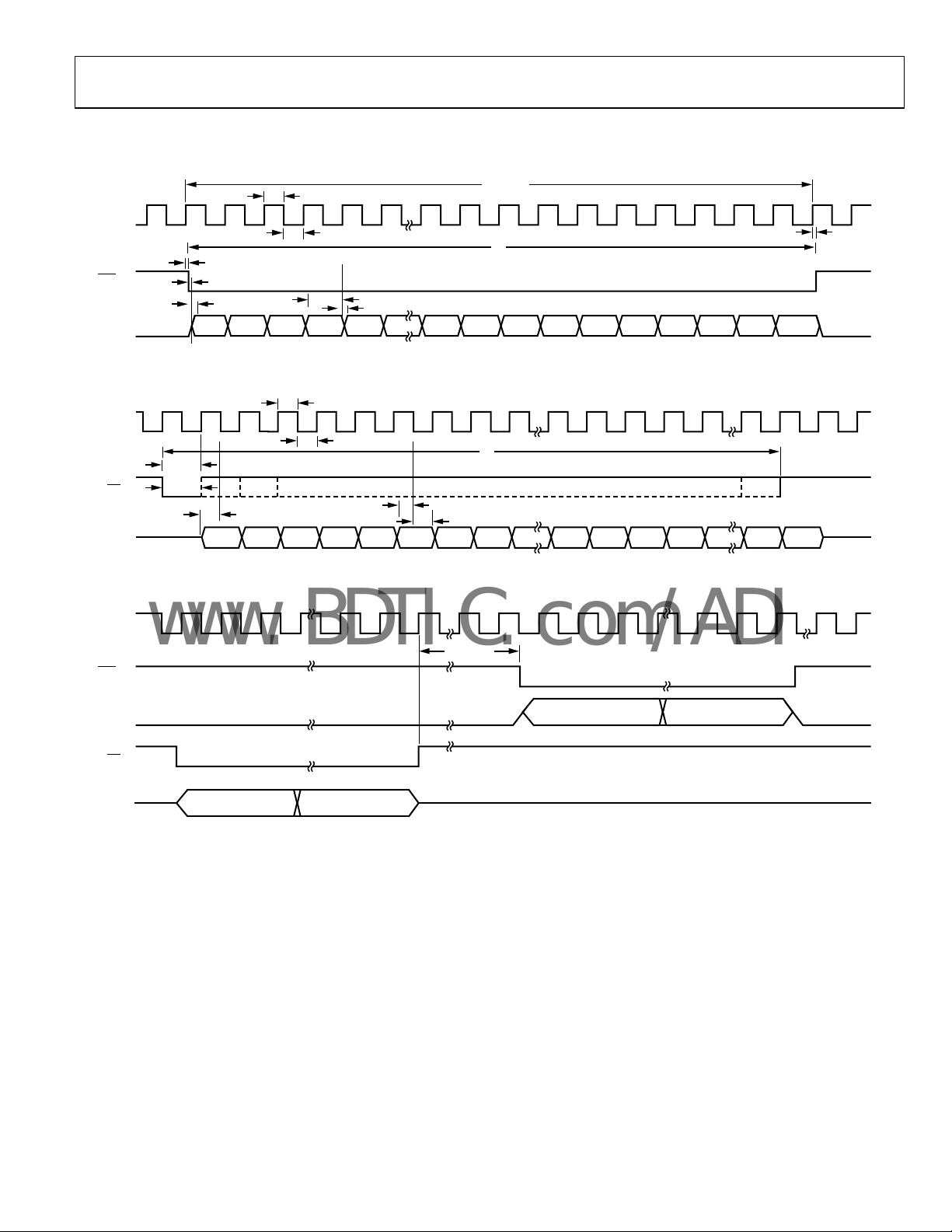
TIMING DIAGRAMS
32 ×
t
SCO
t
t
9
t
12
8
6518-002
06518-003
SCO (O)
FSO (O)
SDO (O)
SCO (O)
FSI (I)
SDI (I)
t
1
t
2
t
3
t
4
t
5
D22D23 D21 D20 D19 D1 D0 ST4 ST 3 ST2 ST 1 ST0 0 0 0
t
6
t
7
Figure 2. Serial Read Timing Diagram
t
1
t
2
t
10
t
11
t
13
RA15 RA14 RA13 RA12 RA11 RA10 RA9 RA8 RA1 RA0 D15 D14 D1 D0
t
14
t
15
Figure 3. AD7764 Register Write
SCO (O)
FSO (O)
SDO (O)
FSI (I)
SDI (I)
CONTROL REG ISTER
ADDR (0x0001)
CONTROL REGISTER
INSTRUCTION
Figure 4. AD7764 Status Register Read Cycle
≥8 ×
t
SCO
STATUS REGISTER
CONTENTS [31:16]
NEXT DATA READ FO LLOW ING THE W RITE TO CONTROL REGISTER
DON’T CARE
BITS [15:0]
06518-004
Rev. 0 | Page 7 of 32
Page 8
AD7764
www.BDTIC.com/ADI
ABSOLUTE MAXIMUM RATINGS
TA = 25°C, unless otherwise noted.
Table 4.
Parameter Rating
AV
1 to GND −0.3 V to +2.8 V
DD
AVDD2, AVDD3, AVDD4 to GND −0.3 V to +6 V
DV
to GND −0.3 V to +2.8 V
DD
VINA+ , VINA− to GND
VIN+ , VIN− to GND
1
−0.3 V to +6 V
1
−0.3 V to +6 V
Digital Input Voltage to GND2 −0.3 V to +2.8 V
V
+ to GND
REF
3
−0.3 V to +6 V
AGND to DGND −0.3 V to +0.3 V
Input Current to Any Pin Except Supplies
Operating Temperature Range
4
±10 mA
Commercial −40°C to +85°C
Storage Temperature Range −65°C to +150°C
Junction Temperature 150°C
TSSOP Package
θ
Thermal Impedance 143°C/W
JA
θ
Thermal Impedance 45°C/W
JC
Lead Temperature, Soldering
Vapor Phase (60 sec) 215°C
Infrared (15 sec) 220°C
ESD 1 kV
1
Absolute maximum voltage for VIN−, VIN+, VINA−, and VINA+ is 6.0 V or
AVDD3 + 0.3 V, whichever is lower.
2
Absolute maximum voltage on digital inputs is 3.0 V or DV
whichever is lower.
3
Absolute maximum voltage on V
whichever is lower.
4
Transient currents of up to 100 mA do not cause SCR latch-up.
+ input is 6.0 V or AVDD4 + 0.3 V,
REF
+ 0.3 V,
DD
Stresses above those listed under Absolute Maximum Ratings
y cause permanent damage to the device. This is a stress
ma
rating only; functional operation of the device at these or any
other conditions above those listed in the operational sections
of this specification is not implied. Exposure to absolute
maximum rating conditions for extended periods may affect
device reliability.
ESD CAUTION
Rev. 0 | Page 8 of 32
Page 9
AD7764
www.BDTIC.com/ADI
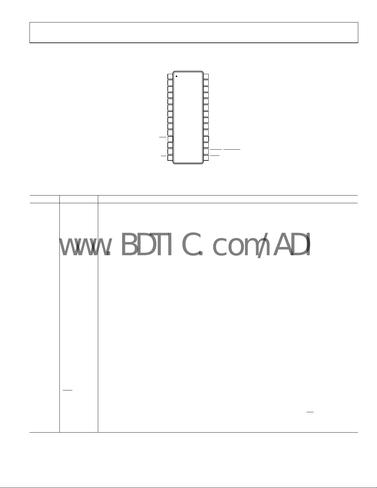
PIN CONFIGURATION AND FUNCTION DESCRIPTIONS
V
IN
V
OUT
V
IN
V
OUT
V
V
AV
DD
AGND3
OVERRANGE
SCO
FSO
SDO
SDI
FSI
A–
A+
A+
A–
–
IN
+
IN
2
1
2
3
4
5
6
AD7764
TOP VIEW
7
(Not to Scale)
8
9
10
11
12
13
14
28
3
AV
DD
27
V
+
REF
26
REFGND
25
AV
4
DD
24
1
AV
DD
23
AGND1
22
R
BIAS
21
AV
2
DD
20
AGND2
19
MCLK
18
DEC_RATE
17
DV
DD
16
RESET/PWRDWN
15
SYNC
06518-005
Figure 5. 28-Lead TSSOP Pin Configuration
Table 5. Pin Function Descriptions
Pin No. Mnemonic Description
24 AVDD1 2.5 V Power Supply for Modulator. This pin should be decoupled to AGND1 (Pin 23) with a 100 nF capacitor.
7 and 21 AVDD2
5 V Power Supply. Pin 7 should be decoupled to AGND3 (P
in 8) with a 100 nF capacitor. Pin 21 should be
decoupled to AGND1 (Pin 23) with a 100 nF capacitor.
28 AVDD3
3.3 V to 5 V Power Supply for Differential Amplifier. This pin shou
ld be decoupled to the ground plane with
a 100 nF capacitor.
25 AVDD4
3.3 V to 5 V Power Supply for Reference Buffer. This pin should be dec
oupled to AGND1 (Pin 23) with a 100 nF
capacitor.
17 DVDD
2.5 V Power Supply for Digital Circuitry and FIR Filter. This pin sh
ould be decoupled to the ground plane with
a 100 nF capacitor.
22 R
BIAS
Bias Current Setting Pin. A resistor must be inserted bet
ween this pin and AGND. For more details, see the
Bias Resistor Selection section.
23 AGND1 Power Supply Ground for Analog Circuitry.
20 AGND2 Power Supply Ground for Analog Circuitry.
8 AGND3 Power Supply Ground for Analog Circuitry.
26 REFGND Reference Ground. Ground connection for the reference voltage.
27 V
+ Reference Input.
REF
1 VINA− Negative Input to Differential Amplifier.
2 V
A+ Positive Output from Differential Amplifier.
OUT
3 VINA+ Positive Input to Differential Amplifier.
4 V
A− Negative Output from Differential Amplifier.
OUT
5 VIN− Negative Input to the Modulator.
6 VIN+ Positive Input to the Modulator.
9 OVERRANGE
Overrange Pin. This pin outputs a logic high to indicate tha
t the user has applied an analog input that is
approaching the limit of the analog input to the modulator.
10 SCO
Serial Clock Out. This clock signal is derived from the int
ernal ICLK signal. The frequency of this clock is equal
to ICLK. See the Clocking the AD7764 section for further details.
11
FSO
12 SDO
Frame Sync Out. This signal frames the ser
Serial Data Out. Data and status are output on this pin during each ser
ial data output and is 32 SCO periods wide.
ial transfer. Each bit is clocked out on an
SCO rising edge and is valid on the falling edge. See the AD7764 Interface section for further details.
13 SDI
Serial Data In. The first data bit (MSB) must be v
alid on the next SCO falling edge after the FSI
event is latched.
32 bits are required for each write; the first 16-bit word contains the device and register address, and the
second word contains the data. See the AD7764 Interface section for further details.
Rev. 0 | Page 9 of 32
Page 10

AD7764
www.BDTIC.com/ADI
Pin No. Mnemonic Description
14
15
16
19 MCLK
18 DEC_RATE
FSI
SYNC
RESET
/
PWRDWN
Frame Sync Input. The status of this pin is checked on the falling edge of SCO. If this pin is low, then the first
data bit is latched in on the next SCO falling edge. See the AD7764 Interface section for further details.
Synchronization Input. A falling edge on this pin resets the internal filter. This can be used to synchronize
multiple devices in a system. See the Synchronization section for further details.
Reset/Power-down Pin. When a logic low is sensed on this pin, the part is powered down and all internal
circuitry is reset.
Master Clock Input. A low jitter digital clock must be applied t
frequency of this clock. See the Clocking the AD7764 section for more details.
Decimation Rate. This pin selects one of the three decimation rate modes. When 2.5 V is applied to this pin,
a decima
decimation rate of 256× is selected by setting the pin to ground.
tion rate 64× is selected. A decimation rate of 128× is selected by leaving the pin floating. A
o this pin. The output data rate depends on the
Rev. 0 | Page 10 of 32
Page 11

AD7764
www.BDTIC.com/ADI
TYPICAL PERFORMANCE CHARACTERISTICS
AVDD1 = DVDD = V
measured to 16-bit accuracy. The input signal is reduced to avoid modulator overload and digital clipping. Fast Fourier transforms (FFTs)
of −0.5 dB tones are generated from 262,144 samples in normal power mode. All other FFTs are generated from 8192 samples.
0
= 2.5 V, AVDD2 = AVDD3 = AVDD4 = 5 V, V
DRIVE
+ = 4.096 V, MCLK amplitude = 5 V, TA = 25°C. Linearity plots are
REF
0
–25
–50
–75
–100
AMPLITUDE (dB)
–125
–150
–175
0 50k 100k 156. 249k
FREQUENCY (Hz)
Figure 6. Normal Power Mode, FFT,1 kHz, −0.5 dB Input Tone,
4× Decimation Rate
6
0
–25
–50
–75
–100
AMPLITUDE (dB)
–125
–25
–50
–75
–100
AMPLITUDE (dB)
–125
–150
–175
0 150k125k100k75k50k25k
06518-006
FREQUENCY (Hz)
06518-212
Figure 9. Low Power Mode, FFT,1 kHz, −0.5 dB Input Tone,
4× Decimation Rate
6
0
–25
–50
–75
–100
AMPLITUDE (dB)
–125
–150
–175
0 20k 40k 60k 78.124k
FREQUENCY (Hz)
Figure 7. Normal Power Mode, FFT,1 kHz, −0.5 dB Input Tone,
8× Decimation Rate
12
0
–25
–50
–75
–100
AMPLITUDE (dB)
–125
–150
–175
0 10k 20k 30k 39.062k
FREQUENCY (Hz)
Figure 8. Normal Power Mode, FFT,1 kHz, −0.5 dB Input Tone,
6× Decimation Rate
25
06518-007
06518-008
Rev. 0 | Page 11 of 32
–150
–175
0 10k 20k 30k 40k 50k 60k 70k
FREQUENCY (Hz)
Figure 10. Low Power Mode, FFT,1 kHz, −0.5 dB Input Tone,
8× Decimation Rate
12
0
–25
–50
–75
–100
AMPLITUDE (dB)
–125
–150
–175
0 5k 10k 15k 20k 25k 30k 35k
FREQUENCY (Hz)
Figure 11. Low Power Mode, FFT,1 kHz, −0.5 dB Input Tone,
6× Decimation Rate
25
06518-211
06518-210
Page 12

AD7764
www.BDTIC.com/ADI
0
0
–25
–50
–75
–100
AMPLITUDE (dB)
–125
–150
–175
0 100k 150k50k
FREQUENCY (Hz)
Figure 12. Normal Power Mode, FFT,1 kHz, −6 dB Input Tone,
6
4× Decimation Rate
0
–25
–50
–75
–100
AMPLITUDE (dB)
–125
–25
–50
–75
–100
AMPLITUDE (dB)
–125
–150
–175
0 100k 150k50k
06518-200
FREQUENCY (Hz)
06518-203
Figure 15. Low Power Mode, FFT,1 kHz, −6 dB Input Tone,
6
4× Decimation Rate
0
–25
–50
–75
–100
AMPLITUDE (dB)
–125
–150
–175
0 50k 75k25k
FREQUENCY (Hz)
Figure 13. Normal Power Mode, FFT,1 kHz, −6 dB Input Tone,
12
8× Decimation Rate
0
–25
–50
–75
–100
AMPLITUDE (dB)
–125
–150
–175
0330k25k20k15k10k5k
FREQUENCY (Hz)
Figure 14. Normal Power Mode, FFT,1 kHz, −6 dB Input Tone,
6× Decimation Rate
25
–150
–175
0 50k 75k25k
06518-201
Figure 16. Low Power Mode, FFT,1 kHz, −6 dB Input Tone,
0
–25
–50
–75
–100
AMPLITUDE (dB)
–125
–150
5k
06518-202
–175
0330k25k20k15k10k5k
Figure 17. Low Power Mode, FFT,1 kHz, −6 dB Input Tone,
FREQUENCY (Hz)
12
8× Decimation Rate
FREQUENCY (Hz)
6× Decimation Rate
25
06518-204
5k
06518-205
Rev. 0 | Page 12 of 32
Page 13

AD7764
www.BDTIC.com/ADI
40
25
35
30
25
20
15
CURRENT (mA)
10
5
0
0 10203045 152535
AV
1
DD
MCLK FREQUENCY ( MHz)
Figure 18. Normal Power Mode, Current Consu
DV
DD
AVDD2
AV
3
DD
AV
mption vs. MCLK Frequency,
4
DD
0
06518-010
64× Decimation Rate
40
35
30
25
20
15
CURRENT (mA)
10
5
0
0102030405152535
MCLK FREQUENCY ( MHz)
AVDD4
AV
DV
DD
1
DD
AVDD2
AVDD3
45
06518-114
Figure 19. Normal Power Mode, Current Consumption vs. MCLK Frequency,
128× Decimation Rate
20
DV
DD
15
AV
1
DD
10
CURRENT (mA)
5
0
0102030405152535
AVDD4
MCLK FREQUENCY ( MHz)
AVDD2
AV
3
DD
45
Figure 21. Low Power Mode, Current Consumption vs. MCLK Frequency,
6
4× Decimation Rate
25
DV
AV
DD
AVDD2
DD
1
AVDD3
45
20
15
10
CURRENT (mA)
5
AVDD4
0
0102030405152535
MCLK FREQUENCY ( MHz)
Figure 22. Low Power Mode, Current Consumption vs. MCLK Frequency,
128× Decimation Rate
06518-011
06518-115
40
35
30
25
20
15
CURRENT (mA)
10
5
0
0 10203045 152535
MCLK FREQUENCY ( MHz)
Figure 20. Normal Power Mode, Current Consu
256× Decimation Rate
DV
DD
1
AV
DD
AVDD2
AVDD3
AVDD4
0
06518-112
mption vs. MCLK Frequency,
20
18
16
14
12
10
8
CURRENT (mA)
6
4
2
0
0 10203045 152535
Figure 23. Low Power Mode, Current Consumption vs. MCLK Frequency,
256× Decimation Rate
Rev. 0 | Page 13 of 32
MCLK FREQUENCY ( MHz)
AVDD1
AVDD4
DV
AVDD2
DD
AVDD3
0
06518-113
Page 14

AD7764
www.BDTIC.com/ADI
2.0
1.5
1.0
0.5
0
DNL (LSB)
–0.5
–1.0
–1.5
–2.0
6k 55k 5953510k 15k 20k 25k 30k 35k 40k 45k 50k
0.00300
0.00225
CODE
Figure 24. DNL Plot
–40°C
0
–20
–40
–60
–80
–100
AMPLITUDE (dB)
–120
–140
–160
–180
0 7812460k40k20k
06518-208
Figure 27. Normal Power Mode, IMD, f
FREQUENCY (Hz)
A = 49.7 kHz, fIN B = 50.3 kHz,
IN
06518-209
50 kHz Center Frequency, 128× Decimation Rate
0.003225
0.003000
+85°C
0.00150
0.00075
0
INL (%)
–0.00075
–0.00150
–0.00225
–0.00300
6k 55k 5953510k 15k 20k 25k 30k 35k 40k 45k 50k
16-BIT CODE SCALING
Figure 25. Normal Power Mode INL
110
109
108
107
106
SNR (dB)
105
104
103
NORMAL SNR
LOW SNR
+25°C
+85°C
0.00225
+25°C
0.00150
INL (%)
0.00075
0
–0.00012
6k 55k 5953510k 15k 20k 25k 30k 35k 40k 45k 50k
06518-206
16-BITCODE SCALING
Figure 28. Low Power Mode INL
–40°C
06518-207
102
0 64 128 192 256
DECIMATIO N RATE
06518-009
Figure 26. Normal and Low Power Mode, SNR vs. Decimation Rate,
1 kHz, −0.5 dB Input Tone
Rev. 0 | Page 14 of 32
Page 15

AD7764
www.BDTIC.com/ADI
TERMINOLOGY
Signal-to-Noise Ratio (SNR)
The ratio of the rms value of the actual input signal to the rms
sum of all other spectral components below the Nyquist frequency, excluding harmonics and dc. The value for SNR is
expressed in decibels (dB).
Total Harmonic Distortion (THD)
T
he ratio of the rms sum of harmonics to the fundamental.
For the AD7764, it is defined as
22222
VVVVV
++++
54
()
THD
where:
V
is the rms amplitude of the fundamental.
1
V
, V3, V4, V5, and V6 are the rms amplitudes of the second
2
to the sixth harmonics.
Nonharmonic Spurious-Free Dynamic Range (SFDR)
The ratio of the rms signal amplitude to the rms value of the
peak spurious spectral component, excluding harmonics.
Dynamic Range
The ratio of the rms value of the full scale to the rms noise
measured with the inputs shorted together. The value for
dynamic range is expressed in decibels.
Intermodulation Distortion
With inputs consisting of sine waves at two frequencies, fa and
fb, any active device with nonlinearities creates distortion products
at sum and difference frequencies of mfa ± nfb, where m, n = 0,
1, 2, 3, and so on. Intermodulation distortion terms are those
for which neither m nor n is equal to 0. For example, the secondorder terms include (fa + fb) and (fa − fb), while the third-order
terms include (2fa + fb), (2fa − fb), (fa + 2fb), and (fa − 2fb).
The AD7764 is tested using the CCIF standard, where two input
frequencies near the top end of the input bandwidth are used.
In this case, the second-order terms are usually distanced in
requency from the original sine waves, and the third-order
f
terms are usually at a frequency close to the input frequencies.
As a result, the second- and third-order terms are specified
separately. The calculation of the intermodulation distortion is
as per the THD specification, where it is the ratio of the rms
sum of the individual distortion products to the rms amplitude
of the sum of the fundamentals expressed in dB.
Integral Nonlinearity (INL)
The maximum deviation from a straight line passing through
the endpoints of the ADC transfer function.
Differential Nonlinearity (DNL)
The difference between the measured and the ideal 1 LSB
change between any two adjacent codes in the ADC.
Zero Error
The difference between the ideal midscale input voltage (when
log20dB
=
32
V
1
6
both inputs are shorted together) and the actual voltage
producing the midscale output code.
Zero Error Drift
The change in the actual zero error value due to a temperature
change of 1°C. It is expressed as a percentage of full scale at
room temperature.
Gain Error
The first transition (from 100…000 to 100…001) should occur
for an analog voltage 1/2 LSB above the nominal negative full
scale. The last transition (from 011…110 to 011…111) should
occur for an analog voltage 1 1/2 LSB below the nominal full
scale. The gain error is the deviation of the difference between
the actual level of the last transition and the actual level of the
first transition, from the difference between the ideal levels.
Gain Error Drift
The change in the actual gain error value due to a temperature
change of 1°C. It is expressed as a percentage of full scale at
room temperature.
Rev. 0 | Page 15 of 32
Page 16

AD7764
www.BDTIC.com/ADI
THEORY OF OPERATION
The AD7764 features an on-chip fully differential amplifier to
feed the Σ- modulator pins , an on-chip reference buffer, and
a FIR filter block to perform the required digital filtering of the
Σ- modulator output. Using this Σ- conversion technique
with the added digital filtering, the analog input is converted to
an equivalent digital word.
Σ-Δ MODULATION AND DIGITAL FILTERING
The input waveform applied to the modulator is sampled and
an equivalent digital word is output to the digital filter at a rate
equal to ICLK. By employing oversampling, the quantization
f
f
ICLK
ICLK
ICLK
/2
/2
. This
06518-012
06518-013
noise is spread across a wide bandwidth from 0 to f
means that the noise energy contained in the signal band of
interest is reduced (see Figure 29). To further reduce the
uantization noise, a high-order modulator is employed to
q
shape the noise spectrum so that most of the noise energy is
shifted out of the signal band (see
QUANTIZAT ION NOIS E
BAND OF INTERE ST
Figure 29. Σ-Δ ADC, Quantization Noise
NOISE SHAPI NG
BAND OF INTERE ST
Figure 30. Σ-Δ ADC, Noise Shaping
Figure 30).
The AD7764 employs three FIR filters in series. By using
dif
ferent combinations of decimation ratios, data can be
obtained from the AD7764 at three data rates.
The first filter receives data from the modulator at ICLK
where it is decimated 4× to output data at (ICLK/4)
MHz
MHz. The
second filter allows the decimation rate to be chosen from
8× to 32×.
The digital filtering on the AD7764 provides full-band filtering.
means that its stop-band attenuation occurs at the Nyquist
This
frequency (ODR/2). This feature provides increased protection
against aliasing of sampled frequencies that lie above the
Nyquist rate (ODR/2). The filter gives maximum attenuation at
the Nyquist rate (see
p
ossible alias frequencies by 110 dB. The frequency response in
Figure 32). This means that it attenuates all
Figure 32 occurs when the AD7764 is operated with a 40 MHz
MCLK i
n the decimate 64× mode. Note that the first stop-band
frequency occurs at Nyquist. The frequency response of the
filter scales with both the decimation rate chosen and the MCLK
frequency applied.
The third filter has a fixed decimation rate of 2×. Tabl e 6 shows
s
ome characteristics of the digital filtering where ICLK =
MCLK/2. The group delay of the filter is defined to be the delay
to the center of the impulse response and is equal to the computation plus the filter delays. The delay until valid data is available
(the FILTER-SETTLE status bit is set) is approximately twice
the filter delay plus the computation delay. This is listed in
terms of MCLK periods in
0
–20
–40
Table 6.
PASS-BAND RIPPL E = 0.05dB
–0.1dB FREQ UENCY = 125.1kHz
–3dB FREQUE NCY = 128kHz
STOP BAND = 156. 25kHz
DIGITAL FILT ER CUTOFF FREQUENCY
f
/2
BAND OF INTERE ST
Figure 31. Σ-Δ ADC, Digital Filter C
utoff Frequency
ICLK
06518-014
The digital filtering that follows the modulator removes the
large out-of-band quantization noise (see Figure 31) while also
r
educing the data rate from f
/64 or less at the output of the filter, depending on the
f
ICLK
at the input of the filter to
ICLK
–60
–80
–100
AMPLITUDE (dB)
–120
–140
–160
0325020015010050
Figure 32. Filter Frequency Resp
decimation rate used.
Table 6. Configuration with Default Filter
SYNC
ICLK
Frequency
Decimation
Rate
Data State
Computation
Delay
Filter Delay
20 MHz 64× Fully filtered 2.25 µs 87.6 µs 7122 × t
20 MHz 128× Fully filtered 3.1 µs 174 µs 14217 × t
20 MHz 256× Fully filtered 4.65 µs 346.8 µs 27895 × t
12.288 MHz 64× Fully filtered 3.66 µs 142.6 µs 7122 × t
12.288 MHz 128× Fully filtered 5.05 µs 283.2 µs 14217 × t
12.288 MHz 256× Fully filtered 7.57 µs 564.5 µs 27895 × t
Rev. 0 | Page 16 of 32
to
FILTER-SETTLE
125 kHz 312.5 kHz
MCLK
62.5 kHz 156.25 kHz
MCLK
31.25 kHz 78.125 kHz
MCLK
76.8 kHz 192 kHz
MCLK
38.4 kHz 96 kHz
MCLK
19.2 kHz 48 kHz
MCLK
FREQUENCY (kHz)
onse (312.5 kHz ODR)
Pass-Band
Bandwidth
00
06518-015
Output Data Rate
DR)
(O
Page 17

AD7764
=
×
R
www.BDTIC.com/ADI
AD7764 INPUT STRUCTURE
The AD7764 requires a 4.096 V input to the reference pin,
+, supplied by a high precision reference, such as the
V
REF
ADR444. Because the input to the device’s Σ- modulator are
fully differential, the effective differential reference range is
8.192 V.
V192.8096.42
V
)(
+ DiffREF
=×=
As is inherent in Σ- modulators, only a certain portion of this
f
ull reference may be used. With the AD7764, 80% of the full
differential reference may be applied to the modulator’s
differential inputs.
OVERRANGE REGION
+4.096V
InputModulator
FULLSCALE
This means that a maximum of ±3.2768 V p-p full-scale can be
a
pplied to each of the AD7764 modulator inputs (Pin 5 and
Pin 6), with the AD7764 being specified with an input −0.5 dB
down from full scale(−0.5 dBFS).
The AD7764 modulator inputs must have a common-mode
put of 2.048 V. Figure 33 shows the relative scaling between
in
he differential voltages applied to the modulator pins, and the
t
respective 24-bit twos complement digital outputs.
TWOS COMPLEMENT
DIGITAL OUTPUTINPUT VOLTAGE (V)
=
V5536.68.0V192.8_
INPUT TO MODULATO
PIN 5 AND PIN 6
V
– AND VIN+
IN
VIN+ = 3.6855V
VIN– = 0.4105V
–0.5dBFS I NPUT
+ = 2.048V
V
IN
V
– = 2.048V
IN
–0.5dBFS I NPUT
+ = 0.4105V
V
IN
– = 3.6855V
V
IN
Figure 33. AD7764 Scaling: Modulator Input Voltage vs. Digital Output Code
+3.2768V = MO DULATOR F ULL-SCAL E = 80% OF 4.096V
80% OF 4.096V = MODULAT OR FULL -SCALE = –3. 2768V
–4.096V
OVERRANGE REGION
0111 1111 1111 1111 1111 1111
0111 1000 1101 0110 1111 1101
0000 0000 0000 0000 0000 0001
0000 0000 0000 0000 0000 0000
1111 1111 1111 1111 1111 1111
1000 0111 0010 1001 0000 0010
1000 0000 0000 0000 0000 0000
DIGITAL OUTPUT
ON SDO PIN
06518-120
Rev. 0 | Page 17 of 32
Page 18

AD7764
www.BDTIC.com/ADI
ON-CHIP DIFFERENTIAL AMPLIFIER
The AD7764 contains an on-board differential amplifier that is
recommended to drive the modulator input pins. Pin 1, Pin 2,
Pin 3, and Pin 4 on the AD7764 are the differential input and
output pins of the amplifier. The external components, R
C
, CS, and RM, are placed around Pin 1 through Pin 6 to create
FB
the recommended configuration.
To achieve the specified performance, the differential amplifier
ld be configured as a first-order antialias filter, as shown in
shou
Figure 34, using the component values listed in Tabl e 7. The
puts to the differential amplifier are then routed through the
in
external component network before being applied to the
modulator inputs, V
− and VIN+, (Pin 5 and Pin 6). Using the
IN
optimal values in the table as an example yields a 25 dB
attenuation at the first alias point of 19.6 MHz.
C
FB
R
FB
R
IN
A
B
R
DIFF
C
S
AMP
IN
R
C
R
M
VIN–
C
M
V
R
FB
FB
M
IN
Figure 34. Differential Amplifier Configuration
Table 7. On-Chip Differential Filter Component Values
R
R
IN
(kΩ)
FB
(kΩ)
RM
(Ω)
CS
(pF)
CFB
(pF)
Optimal 4.75 3.01 43 8.2 47 33
Tolerance
Range
1
Values shown are the acceptable tolerances for each component when
2.37 to
1
76
5.
2.4 to
4.87
36 to
47
0 to
10
20 to
100
altered relative to the optimal values used to achieve the stated
specifications of the device.
The range of values for each of the components in the
differential amplifier configuration is listed in Tab le 7. When
usin
g the differential amplifier to gain the input voltages to the
required modulator input range, it is advisable to implement the
gain function by changing R
and leaving the RFB as the listed
IN
optimal value.
, RFB,
IN
+
6518-024
CM
(pF)
39 to 56
The common-mode input at each of the differential amplifier
in
puts (Pin V
A+ and Pin VINA−) can range from −0.5 V dc to
IN
2.2 V dc. The amplifier has a constant output common-mode
voltage of 2.048 V, that is, V
voltage for the modulator input pins (V
/2, the requisite common mode
REF
+ and VIN−).
IN
Figure 35 shows the signal conditioning that occurs using the
ferential amplifier configuration detailed in Table 7 with a
dif
±2.5 V in
put signal to the differential amplifier. The amplifier in
this example is biased around ground and is scaled to provide
±3.168 V p-p (−0.5 dBFS) on each modulator input with a
2.048 V common mode.
+2.5V
0V
A
–2.5V
+2.5V
B
0V
–2.5V
Figure 35. Differential Amplifier Signal Conditioning
+3.632V
+2.048V
+0.464V
+3.632V
+2.048V
+0.464V
VIN+
V
–
IN
To obtain maximum performance from the AD7764, it is advisable
to drive the ADC with differential signals. Figure 36 shows how a
ipolar, single-ended signal biased around ground can drive the
b
AD7764 with the use of an external op amp, such as the AD8021.
C
FB
2R
V
IN
2R
AD8021
R
Figure 36. Single-Ended-to-D
R
R
ifferential Conversion
R
FB
IN
DIFF
C
S
AMP
R
IN
C
R
M
VIN–
C
M
R
M
VIN+
FB
FB
6518-122
6518-026
Rev. 0 | Page 18 of 32
Page 19

AD7764
V
www.BDTIC.com/ADI
MODULATOR INPUT STRUCTURE
The AD7764 employs a double-sampling front end, as shown in
Figure 37. For simplicity, only the equivalent input circuitry for
is shown. The equivalent circuitry for VIN− is the same.
V
IN+
+
IN
CPA
SS1
SH1
SS2
SH2
Figure 37. Equivalent Input Circuit
CPB1
CPB2
CS1
CS2
SS3
SS4
SH3
SH4
ANALOG
MODULATOR
06518-027
Sampling Switches SS1 and SS3 are driven by ICLK, whereas
ICLK
Sampling Switches SS2 and SS4 are driven by
. When
ICLK is high, the analog input voltage is connected to CS1. On
the falling edge of ICLK , the SS1 and SS3 switches open and the
analog input is sampled on CS1. Similarly, when ICLK is low,
the analog input voltage is connected to CS2. On the rising edge
of ICLK, the SS2 and SS4 switches open, and the analog input is
sampled on CS2.
Capacitors CPA, CPB1, and CPB2 represent parasitic capacitance
s that include the junction capacitances associated with the
MOS switches.
Table 8. Equivalent Component Values
CS1 CS2 CPA CPB1/2
13 pF 13 pF 13 pF 5 pF
Rev. 0 | Page 19 of 32
Page 20

AD7764
www.BDTIC.com/ADI
AD7764 INTERFACE
READING DATA
The AD7764 uses an SPI-compatible serial interface. The
timing diagram in Figure 2 shows how the AD7764 transmits its
c
onversion results.
The data read from the AD7764 is clocked out using the serial
lock output (SCO). The SCO frequency is half that of the
c
MCLK input to the AD7764.
The conversion result output on the serial data output (SDO)
ramed by the frame synchronization output,
line is f
is sent logic low for 32 SCO cycles. Each bit of the new
conversion result is clocked onto the SDO line on the rising
SCO edge and is valid on the falling SCO edge. The 32-bit result
consists of the 24 data bits followed by five status bits followed
further by three zeros. The five status bits are listed in Tabl e 9
nd described below the table.
a
Table 9. Status Bits During Data Read
D7 D6 D5 D4 D3
FILTER-SETTLE OVR LPWR DEC_RATE 1 DEC_RATE 0
• The FILTER-SETTLE bit indicates whether the data output
from the AD7764 is valid. After resetting the device (using
the
SYNC
indicate that the full settling time of the filter has not yet
passed and that the data is not yet valid. The FILTERSETTLE bit also goes to zero when the input to the part
has asserted the overrange alerts.
• The OVR (overrange) bit is described in the Overrange
Alerts
• The LPWR bit is set to logic high when the AD7764 is
operating in low power mode. See the Power Modes
sectio
• The DEC_RATE 1 and DEC_RATE 0 bits indicate the
decimation ratio used. Tab le 1 0 is a truth table for the
ecimation rate bits.
d
Table 10. Decimation Rate Status Bits
Decimate DEC_RATE 1 DEC_RATE 0
64× 0 1
1281× 1 X
256× 0 0
1
Don’t care. If the DEC_RATE 1 bit is set to 1, AD7764 is in Decimate
128× mode.
pin) or clearing the digital filter (using the
RESET
pin), the FILTER-SETTLE bit goes logic low to
section.
n for further details.
FSO
, which
READING STATUS AND OTHER REGISTERS
The AD7764 features a gain correction register, an overrange
register, and a read-only status register. To read back the
contents of these registers, the user must first write to the
control register of the device, and set the bit that corresponds to
the register to be read. The next read operation outputs the
contents of the selected register (on the SDO pin) instead of a
conversion result.
To ensure that the next read cycle contains the contents of the
r
egister written to, the write operation to that register must be
completed a minimum of 8 × t
which indicates the start of the next read cycle. See Figure 4 for
fu
rther details.
The AD7764 Registers section provides more information on
he relevant bits in the control register.
t
before the falling edge of
SCO
FSO
WRITING TO THE AD7764
A write operation to the AD7764 is shown in Figure 3. The
serial writing operation is synchronous to the SCO signal. The
FSI
status of the frame synchronization input,
falling edge of the SCO signal. If the
first data bit on the serial data in (SDI) line is latched in on the
next SCO falling edge.
FSI
Set the active edge of the
the SCO signal is high or low to allow setup and hold times
from the SCO falling edge to be met. The width of the
signal can be set to between 1 and 32 SCO periods wide. A
s
econd, or subsequent, falling edge that occurs before
32 SCO periods have elapsed, is ignored.
Figure 3 details the format for the serial data being written to
e AD7764 through the SDI pin. Thirty-two bits are required
th
for a write operation. The first 16 bits are used to select the
register address that the data being read is intended for. The
second 16 bits contain the data for the selected register.
Writing to the AD7764 is allowed at any time, even while
re
ading a conversion result. Note that after writing to the
devices, valid data is not output until after the settling time for
the filter has elapsed. The FILTER-SETTLE status bit is asserted
at this point to indicate that the filter has settled and that valid
data is available at the output.
signal to occur at a position when
FSI
, is checked on the
line is low, then the
FSI
,
Rev. 0 | Page 20 of 32
Page 21

AD7764
C
T
www.BDTIC.com/ADI
AD7764 FUNCTIONALITY
SYNCHRONIZATION
SYNC
The
input to the AD7764 provides a synchronization
function that allows the user to begin gathering samples of the
analog front-end input from a known point in time.
SYNC
The
the same master clock, that use common
function allows multiple AD7764s, operated from
SYNC
and
RESET
signals to be synchronized so that each ADC simultaneously
updates its output register.
and
RESET
signals to all
SYNC
Connect common MCLK,
SYNC
AD7764 devices in the system. On the falling edge of the
signal, the digital filter sequencer is reset to 0. The filter is held
SYNC
in a reset state until a rising edge of the SCO senses
Thus, to perform a synchronization of devices, a
SYNC
high.
pulse of
a minimum of 2.5 ICLK cycles in length can be applied,
synchronous to the falling edge of SCO. On the first rising edge
SYNC
of SCO after
goes logic high, the filter is taken out of reset,
and the multiple parts gather input samples synchronously.
Following a
SYNC
, the digital filter needs time to settle before
valid data can be read from the AD7764. The user knows there
is valid data on the SDO line by checking the FILTER-SETTLE
status bit (see D7 in Table 9) that is output with each conversion
SYNC
esult. The time from the rising edge of
r
until the FILTERSETTLE bit asserts depends on the filter configuration used. See
the Theory of Operation section and the values listed in Table 6
f
or details on calculating the time until FILTER-SETTLE
asserts. Note that the FILTER_SETTLE bit is designed as a
reactionary flag to indicate when the conversion data output
is valid.
OVERRANGE ALERTS
The AD7764 offers an overrange function in both a pin and
status bit output. The overrange alerts indicate when the voltage
applied to the AD7764 modulator input pins exceeds the limit
set in the overrange register, indicating that the voltage applied
is approaching a level where the modulator will be overranged.
To set this limit, the user must program the register. The default
overrange limit is set to 80% of the V
AD7764 Registers section).
The OVERRANGE pin outputs logic high to alert the user
t
hat the modulator has sampled an input voltage greater in
magnitude than the overrange limit as set in the overrange
register. The OVERRANGE pin is set to logic high when the
modulator samples an input above the overrange limit. Once
the input returns below the limit, the OVERRANGE pin returns
to zero. The OVERRANGE pin is updated after the first FIR
filter stage. Its output changes at the ICLK/4 frequency.
The OVR status bit is output as Bit D6 on SDO during a data
nversion, and can be checked in the AD7764 status register.
co
This bit is less dynamic than the OVERRANGE pin output. It is
updated on each conversion result output, that is, the bit
voltage (see the
REF
changes at the output data rate. If the modulator has sampled a
voltage input that exceeded the overrange limit during the
process of gathering samples for a particular conversion result
output, then the OVR bit is set to logic high.
LOGI
LEVEL
HI
LO
OUTPUT
OVERRANGE PIN
OUTPUT FREQUENCY
OF FIR FILTER 1 = ICLK/4
LOGIC
LEVEL
HI
LO
OVR BIT
Figure 38. OVERRANGE Pin and OVR Bi
Applied to Modulator
OUTPUT DATA RATE (ODR)
(ICLK/DECIMATION RATE
t vs. Absolute Voltage
t
OVERRANGE
LIMIT
OBSOLUTE INPU
TO AD7764
[(V
+) – (VIN–)]
IN
OVERRANGE
LIMIT
t
06518-016
The output points from FIR Filter 1 in Figure 38 are not drawn
to scale relative to the output data rate points. The FIR Filter 1
output is updated either 16×, 32×, or 64× faster than the output
data rate depending on the decimation rate in operation.
POWER MODES
During power-up, the AD7764 defaults to operate in normal
power mode. There is no register write required.
The AD7764 also offers low power mode. To operate the device
in lo
w power mode, the user sets the LPWR bit in the control
register to logic high (See Figure 39). Operating the AD7764 in
ow power mode has no impact on the output data rate or
l
available bandwidth.
SCO (O)
32 ×
t
SCO
FSI (I)
SDI (I)
The AD7764 features a
input to this pin logic low places the AD7764 in power-down
mode. All internal circuitry is reset. To utilize the
functionality, pulse the input to this pin low for a minimum of
one MCLK period. This action resets the internal circuitry.
When the AD7764 receives a logic high input on the
PWRDWN
CONTROL REGISTE R
ADDRESS 0x0001
Figure 39. Write Scheme for Low Power Mode
RESET/PWRDWN
LOW PO WER MODE
DATA 0x0010
pin. Holding the
pin, the device powers up.
RESET
RESET
/
6518-017
Rev. 0 | Page 21 of 32
Page 22

AD7764
www.BDTIC.com/ADI
DECIMATION RATE PIN
The decimation rate of the AD7764 is selected using the
DEC_RATE pin. Tabl e 11 shows the voltage input settings
r
equired for each of the three decimation rates.
Table 11 DEC_RATE Pin Settings
Decimate DEC_RATE Pin Max Output Data Rate
64× DVDD 312.5 kHz
128× Floating 156.25 kHz
256× GND 78.125 kHz
Rev. 0 | Page 22 of 32
Page 23

AD7764
www.BDTIC.com/ADI
DAISY CHAINING
Daisy chaining devices allows numerous devices to use the
same digital interface lines. This feature is especially useful for
reducing component count and wiring connections, such as
in isolated multiconverter applications or for systems with a
limited interfacing capacity. Data readback is analogous to
clocking a shift register.
The block diagram in Figure 40 shows how to connect devices
to
achieve daisy-chain functionality. Figure 40 shows four
AD7764
devices daisy-chained together with a common
MCLK signal applied. This can only work in decimate 128× or
256× modes.
READING DATA IN DAISY-CHAIN MODE
Referring to Figure 40, note that the SDO line of AD7764 (A)
provides the output data from the chain of AD7764 converters.
Also, note that for the last device in the chain, AD7764 (D), the
SDI pin is connected to ground. All of the devices in the chain
SYNC
must use common MCLK and
To enable the daisy-chain conversion process, apply a common
SYNC
pulse to all devices (see the Synchronization section).
After applying a
SYNC
pulse to all devices, the filter settling
time must pass before the FILTER-SETTLE bit is asserted
indicating valid conversion data at the output of the chain of
devices. As shown in Figure 41, the first conversion result is
utput from the device labeled AD7764 (A). This 32-bit
o
conversion result is then followed by the conversion results
signals.
from the devices AD7764 (B), AD7764 (C), and AD7764 (D),
respectively with all conversion results output in an MSB first
sequence. The signals output from the daisy chain are the
stream of conversion results from the SDO pin of AD7764 (A)
FSO
and the
signal output by the first device in the chain,
AD7764 (A).
FSO
The falling edge of
output in the chain.
signals the MSB of the first conversion
FSO
stays logic low throughout the 32 SCO
clock periods needed to output the AD7764 (A) result and then
goes logic high during the output of the conversion results from
the devices AD7764 (B), AD7764 (C), and AD7764 (D).
The maximum number of devices that can be daisy-chained is
endent on the decimation rate selected. Calculate the
dep
maximum number of devices that can be daisy chained by
simply dividing the chosen decimation rate by 32 (the number
of bits that must be clocked out for each conversion). Table 12
rovides the maximum number of chained devices for each
p
decimation rate.
Table 12. Maximum Chain Length for all Decimation Rates
Decimation Rate Maximum Chain Length
256× 8
128× 4
64× 2
SCO
SDO (A)
FSO (A)
SDI (A) = SDO (B)
SDI (B) = SDO (C)
SDI (C) = SDO (D)
FSI
SYNC
MCLK
AD7764
(D)
FSI
SDI
SDO
SYNC
MCLK
Figure 40. Daisy-Chaining Four Devices in Decimate 128× Mode Using a 40 MHz MCLK Signal
32 ×
t
SCO
AD7764 (A)
32-BIT OUTPUT
AD7764 (B) AD7764 (C) AD7764 (D) AD7764 (B) AD7764 (C)
AD7764 (C) AD7764 (D) AD7764 (C) AD7764 (D)
AD7764 (D) AD7764 (D)
32 ×
AD7764 (B)
32-BIT OUTPUT
Figure 41. Daisy-Chain Mode, Data Read Timing Diagram
(for D
AD7764
(C)
FSI
SDI
SDO
SYNC
MCLK
t
SCO
aisy-Chain Configuration Shown in Figure 40)
32 ×
t
SCO
AD7764 (C)
32-BIT OUTPUT
AD7764
(B)
FSI
SDI
SYNC
MCLK
SDO
32 ×
AD7764 (D)
32-BIT OUTPUT
t
SCO
AD7764
(A)
FSI
SDI
SDO
SYNC
MCLK
AD7764 (A)
32-BIT OUTPUT
FSO
06518-018
AD7764 (B)
32-BIT OUTPUT
06518-019
Rev. 0 | Page 23 of 32
Page 24

AD7764
www.BDTIC.com/ADI
WRITING DATA IN DAISY-CHAIN MODE
Writing to AD7764 devices in daisy-chain mode is similar to
writing to a single device. The serial writing operation is
synchronous to the SCO signal. The status of the frame synchro-
FSI
nization input,
signal. If the
data in the SDI line is latched in on the next SCO falling edge.
Writing data to the AD7764 in daisy-chain mode operates with
th
e same timing structure as writing to a single device (see
Figure 3). The difference between writing to a single device and
iting to a number of daisy-chained devices is in the imple-
wr
mentation of the
the daisy chain determines the period for which the
must remain logic low. To write to n number of devices in the
daisy chain, the period between the falling edge of
, is checked on the falling edge of the SCO
FSI
line is low, then the first data bit on the serial
FSI
signal. The number of devices that are in
FSI
FSI
FSI
AD7764
(D)
FSI
SDI
SDI
SDO
SYNC
MCLK
signal
and the
AD7764
(C)
FSI
SDI
SYNC
MCLK
SDO
rising edge of
FSI
must be between 32 × (n−1) to 32 × n SCO
periods. For example, if three AD7764 devices are being written
FSI
to in daisy-chain mode,
is logic low for between
32 × (3−1) to 32 × 3 SCO pulses. This means that the rising
th
edge of FSI must occur between the 64
and 96th SCO period.
The AD7764 devices can be written to at any time. The falling
FSI
ed
ge of
pin. In the case of a daisy chain, the
overrides all attempts to read data from the SDO
FSI
signal remaining logic
low for more than 32 SCO periods indicates to the AD7764
device that there are more devices further on in the chain. This
means the AD7764 directs data that is input on the SDI pin to
its SDO pin. This ensures that data is passed to the next device
in the chain.
AD7764
(B)
FSI
SDI
SYNC
MCLK
SDO
AD7764
(A)
FSI
SDI
SYNC
MCLK
FSO
SDO
SCO
FSI
SCO
SDI (D)
SDI (C) = SDO (D)
SDI (B) = SDO (C)
SDI (A) = SDO (B)
SYNC
MCLK
Figure 42. Writing to AD7764 Daisy-Chain Configuration
t
10
32 ×
t
SCO
SDI (D)
Figure 43. Daisy-Chain Write Timing Diagram; Writing to Four AD7764 Devices
32 ×
SDI (C)
t
SCO
SDI (B)
32 ×
06518-020
t
SCO
31 ×
SDI (A)
t
SCO
06518-021
Rev. 0 | Page 24 of 32
Page 25

AD7764
www.BDTIC.com/ADI
CLOCKING THE AD7764
The AD7764 requires an external low jitter clock source. This
signal is applied to the MCLK pin. An internal clock signal
(ICLK) is derived from the MCLK input signal. The ICLK
controls the internal operation of the AD7764. The maximum
ICLK frequency is
20 MHz. To gen erat e th e IC LK
ICLK = MCLK/2
For output data rates equal to those used in audio systems, a
12.288 MHz ICLK frequency can be used. As shown in Tabl e 6,
output data rates of 96 kHz and 48 kHz are achievable with this
ICLK frequency.
MCLK JITTER REQUIREMENTS
The MCLK jitter requirements depend on a number of factors
and are given by
=
t
)(
rmsj
The input amplitude also has an effect on these jitter figures.
or example, if the input level is 3 dB below full-scale, the
F
allowable jitter is increased by a factor of √2, increasing the first
example to 57.75 ps rms. This happens when the maximum
slew rate is decreased by a reduction in amplitude.
Figure 44 and Figure 45 illustrate this point, showing the
imum slew rate of a sine wave of the same frequency, but
max
with different amplitudes.
1.0
256
ps470
=
45.53
10102.192
×××π×
=
t
)(
rmsj
OSR
)(
102
××π×
f
IN
dBSNR
20
where:
R = oversampling ratio = f
OS
f
= maximum input frequency.
IN
ICLK
/ODR.
SNR(dB) = target SNR.
Example 1
This example can be taken from Table 6, where:
ODR = 312.5 kH
= 20 MHz.
f
ICLK
f
(max) = 156.25 kHz.
IN
z.
SNR = 104 dB.
=
)(
rmsj
64
2.53
101025.1562
×××π×
pst
41.51
=
This is the maximum allowable clock jitter for a full-scale,
156.25 kH
z input tone with the given ICLK and output
data rate.
Example 2
Take a seco nd e xamp le f rom Table 6, where:
ODR = 48 kH
= 12.288 MHz.
f
ICLK
f
(max) = 19.2 kHz.
IN
z.
SNR = 109 dB.
0.5
0
–0.5
–1.0
Figure 44. Maximum Slew Rate of Sine Wave
with
Amplitude of 2 V p-p
1.0
0.5
0
–0.5
–1.0
Figure 45. Maximum Slew Rate of Same Frequency Sine Wave
with
Amplitude of 1 V p-p
06518-022
06518-023
Rev. 0 | Page 25 of 32
Page 26

AD7764
www.BDTIC.com/ADI
DECOUPLING AND LAYOUT INFORMATION
SUPPLY DECOUPLING
The decoupling of the supplies applied to the AD7764 is
important in achieving maximum performance. Each supply
pin must be decoupled to the correct ground pin with a 100 nF,
0603 case size capacitor.
Pay particular attention to decoupling Pin 7 (AV
the nearest ground pin (Pin 8). The digital ground pin AGND2
(Pin 20) is routed directly to ground. Also, connect REFGND
(Pin 26) directly to ground.
The DV
(Pin 17) and AVDD3 (Pin 28) supplies should be
DD
decoupled to the ground plane at a point away from the device.
It is advised to decouple the supplies that are connected to the
lowing supply pins through 0603 size, 100 nF capacitors to a
fol
star ground point linked to Pin 23 (AGND1):
V
AV
AV
AV
+ (Pin 27)
REF
4 (Pin 25)
DD
1 (Pin 24)
DD
2 (Pin 21)
DD
•
•
•
•
A layout decoupling scheme for the these supplies, which
nnect to the right hand side of the AD7764, is shown in
co
Figure 46. Note the star-point ground created at Pin 23.
AV
4
DD
(PIN 25)
PIN 23
TAR-POINT
S
GND
GND
PIN 15
Figure 46. Supply Decoupling
GND
AVDD3 (PIN 28)
V
+ (PIN 27)
REF
AVDD1 (PIN 24)
AVDD2 (PIN 21)
VIA TO GND
FROM PIN 20
REFERENCE VOLTAGE FILTERING
A low noise reference source, such as the ADR444 or ADR34
(4.096 V), is suitable for use with the AD7764. The reference
voltage supplied to the AD7764 should be decoupled and
filtered as shown in
The recommended scheme for the reference voltage supply
is a 200 s
eries resistor connected to a 100 F tantalum
capacitor, followed by a 10 nF decoupling capacitor very close to
the V
REF
+ pin.
Figure 47.
2) directly to
DD
06518-133
ADR444
7.5V VOUT
+
10µF 100nF
2
+VIN
GND
4
Figure 47. Reference Connection
200Ω
6
+
100µF
100nF
V
REF
PIN 27
+
06518-134
DIFFERENTIAL AMPLIFIER COMPONENTS
The components recommended for use around the on-chip
differential amplifier are detailed in Tab le 7 . Matching the
co
mponents on both sides of the differential amplifier is
important to minimize distortion of the signal applied to the
amplifier. A tolerance of 0.1% or better is required for these
components. Symmetrical routing of the tracks on both sides of
the differential amplifier also assists in achieving stated
performance. Figure 48 shows a typical layout for the
co
mponents around the differential amplifier. Note that the
traces for both differential paths are made as symmetrical as
possible and the feedback resistors and capacitors are placed on
the underside of the PCB to enable the simplest routing.
R
IN
R
FB
C
VINA–
VINA+
R
IN
Figure 48. Typical Layout Structure for Surrounding Components
FB
06518-135
LAYOUT CONSIDERATIONS
While using the correct components is essential to achieve
optimum performance, the correct layout is equally as
important. The AD7764 product page on www.analog.com
contains the Gerber files for the AD7764 evaluation board. The
Gerber files should be used as a reference when designing any
system using the AD7764.
The use of ground planes should be carefully considered. To
sure that the return currents through the decoupling
en
capacitors are flowing to the correct ground pin, the ground
side of the capacitors should be as close to the ground pin
associated with that supply as recommended in the
upling section.
Deco
Supply
Rev. 0 | Page 26 of 32
Page 27

AD7764
www.BDTIC.com/ADI
USING THE AD7764
Step1 through Step 5 detail the sequence for powering up and
using the AD7764.
Apply power to the device.
1.
Start the clock oscillator, applying MCLK.
2.
Ta ke
3.
4.
Wait a minimum of two MCLK cycles after
If multiple parts are being synchronized, a
5.
RESET
low for a minimum of one MCLK cycle.
been released.
must be applied to the parts. Otherwise, no
required.
SYNC
When applying the
The application of a
•
not coincide with a write to the device.
Ensure that the
•
minimum of 2.5 ICLK cycles.
pulse
SYNC
pulse to the device must
SYNC
pulse is taken low for a
RESET
SYNC
SYNC
has
pulse
pulse is
Data can then be read from the device using the default gain
nd overrange threshold values. The conversion data read is not
a
valid, however, until the settling time of the filter has elapsed.
Once this has occurred, the FILTER-SETTLE status bit is set
indicating that the data is valid.
Values for gain and overrange thresholds can be written to or
ad from the respective registers at this stage.
re
BIAS RESISTOR SELECTION
The AD7764 requires a resistor to be connected between the
and AGND pins. The resistor value should be selected to
R
BIAS
give a current of 25 µA through the resistor to ground. For a
4.096 V reference voltage, the correct resistor value is 160 kΩ.
Rev. 0 | Page 27 of 32
Page 28

AD7764
www.BDTIC.com/ADI
AD7764 REGISTERS
The AD7764 has a number of user-programmable registers. The control register is used to set the functionality of the on-chip buffer and
differential amplifier and provides the option to power down the AD7764. There are also digital gain and overrange threshold registers.
Writing to these registers involves writing the register address followed by a 16-bit data word. The register addresses, details of individual
bits, and default values are provided in this section.
CONTROL REGISTER
Table 13. Control Register (Address 0x0001, Default Value 0x0000)
MSB LSB
D15 D14 D13 D12 D11 D10 D9 D8 D7 D6 D5 D4 D3 D2 D1 D0
0
RD
OVR
RD
GAIN
0
RD
ST
0 SYNC 0
AT
BYPASS
REF
Table 14. Bit Descriptions of Control Register
Bit Mnemonic Comment
14 RD OVR
13 RD GAIN
11 RD STAT
9 SYNC1
7 BYPASS REF Bypass Reference. Setting this bit bypasses the reference buffer if the buffer is off.
3 PWR DOWN Power Down. A logic high powers the device down without resetting. Writing a 0 to this bit powers the device back up.
2 LPWR Low Power Mode. Set to Logic 1 when AD7764 is in low power mode.
1 REF BUF OFF Reference Buffer Off. Asserting this bit powers down the reference buffer.
0 AMP OFF Amplifier Off. Asserting this bit switches the differential amplifier off.
1
Bit 14 to Bit 11 and Bit 9 are self-clearing bits.
2
Only one of the bits can be set in any write operation because it determines the contents of the next read operation.
1, 2,
Read Overrange. If this bit is set, the next read operation outputs the c
instead of a conversion result.
1, 2
Read Gain. If this bit is set, the next read operation outputs the contents of the digital gain register.
1, 2
Read Status. If this bit is set, the next read operation outputs the contents of the status register.
Synchronize. Setting this bit initiates an internal synchroniz
devices synchronizes all filters.
0 0 0
ation routine. Setting this bit simultaneously on multiple
PWR
DOWN
ontents of the overrange threshold register
LPWR
REF BUF
OFF
AMP
OFF
STATUS REGISTER
Table 15. Status Register (Read Only)
MSB LSB
D15 D14 D13 D12 D11 D10 D9 D8 D7 D6 D5 D4 D3 D2 D1 D0
PARTNO 1 0 0 0
FILTER-
TTLE
SE
0 OVR 0 1 0
REF BUF
ON
AMP
ON
Table 16. Bit Descriptions of Status Register
Bit Mnemonic Comment
15 PARTNO Part Number. This bit is set to one for the AD7764.
10
9 0 Zero. This bit is set to Logic 0.
8 OVR Overrange. If the current analog input exceeds the current overrange threshold, this bit is set.
4 REF BUF ON Reference Buffer On. This bit is set when the reference buffer is in use.
3 AMP ON Amplifier On. This bit is set when the input amplifier is in use.
2 LPWR Low power mode. This bit is set when operating in low power mode.
1 to 0 DEC[1:0] Decimation Rate. These bits correspond to decimation rate in use.
FILTER-
TTLE
SE
Filter Settling Bit. This bit corresponds to the FILTER-SETTLE bit in the status word output in the second 16-bit read
operation. It indicates when data is valid.
LPWR DEC 1 DEC 0
Rev. 0 | Page 28 of 32
Page 29

AD7764
www.BDTIC.com/ADI
GAIN REGISTER—ADDRESS 0x0004
Non-Bit-Mapped, Default Value 0xA000
The gain register is scaled such that 0x8000 corresponds to a
gain of 1.0. The default value of this register is 1.25 (0xA000).
This results in a full-scale digital output when the input is at
80% of V
±80% of V
, tying in with the maximum analog input range of
REF
p-p.
REF
OVERRANGE REGISTER—ADDRESS 0x0005
Non-Bit-Mapped, Default Value 0xCCCC
The overrange register value is compared with the output of the
first decimation filter to obtain an overload indication with
minimum propagation delay. This is prior to any gain scaling.
The default value is 0xCCCC, which corresponds to 80% of
V
(the maximum permitted analog input voltage) Assuming
REF
= 4.096 V, the bit is then set when the input voltage exceeds
V
REF
approximately 6.55 V p-p differential. The overrange bit is set
immediately if the analog input voltage exceeds 100% of V
for more than four consecutive samples at the modulator rate.
REF
Rev. 0 | Page 29 of 32
Page 30

AD7764
C
Y
www.BDTIC.com/ADI
OUTLINE DIMENSIONS
9.80
9.70
9.60
PIN 1
0.15
0.05
OPLANARIT
0.10
28
0.65
BSC
0.30
0.19
COMPLIANT TO JEDEC STANDARDS MO-153-AE
1.20 MAX
SEATING
PLANE
15
4.50
4.40
4.30
0.20
0.09
6.40 BSC
8°
0°
0.75
0.60
0.45
141
Figure 49. 28-Lead Thin Shrink Small Outline [TSSOP]
(R
U-28)
Dimensions shown in millimeters
ORDERING GUIDE
Model Temperature Range Package Description Package Option
AD7764BRUZ1 –40°C to +85°C 28-Lead Thin Shrink Small Outline [TSSOP] RU-28
AD7764BRUZ-REEL71 –40°C to +85°C 28-Lead Thin Shrink Small Outline [TSSOP] RU-28
EVAL-AD7764EBZ1 Evaluation Board
1
Z = RoHS Compliant Part.
Rev. 0 | Page 30 of 32
Page 31

AD7764
www.BDTIC.com/ADI
NOTES
Rev. 0 | Page 31 of 32
Page 32

AD7764
www.BDTIC.com/ADI
NOTES
©2007 Analog Devices, Inc. All rights reserved. Trademarks and
registered trademarks are the property of their respective owners.
D06518-0-6/07(0)
Rev. 0 | Page 32 of 32
 Loading...