

Page 1
8-Bit 20 MSPS, 60 mW
1
2
7
8
3
4
5
6
9
10
151614
13
12
11
19
20
17
18
21
24
23
22
CLOCK LOGIC
FINE COMPARATORS
BANK B
FINE COMPARATORS
BANK A
COARSE
COMPARATORS
CORRECTION LOGIC
AV
DD
AV
SS
3-STATE OUTPUT LATCHES
D7 (MSB)
D0 (LSB)
RREF
15
SWITCH
MATRIX
V
RTS
V
RT
V
RB
V
RBS
OE
AV
SS
CLK DV
SS
AV
DD
V
IN
DV
DD
AD775
4
8
5
255
LSB MULTIPLEXOR
a
FEATURES
CMOS 8-Bit 20 MSPS Sampling A/D Converter
Low Power Dissipation: 60 mW
+5 V Single Supply Operation
Differential Nonlinearity: 0.3 LSB
Differential Gain: 1%
Differential Phase: 0.5 Degrees
Three-State Outputs
On-Chip Reference Bias Resistors
Adjustable Reference Input
Video Industry Standard Pinout
Small Packages:
24-Pin 300 Mil SOIC Surface Mount
24-Pin 400 Mil Plastic DIP
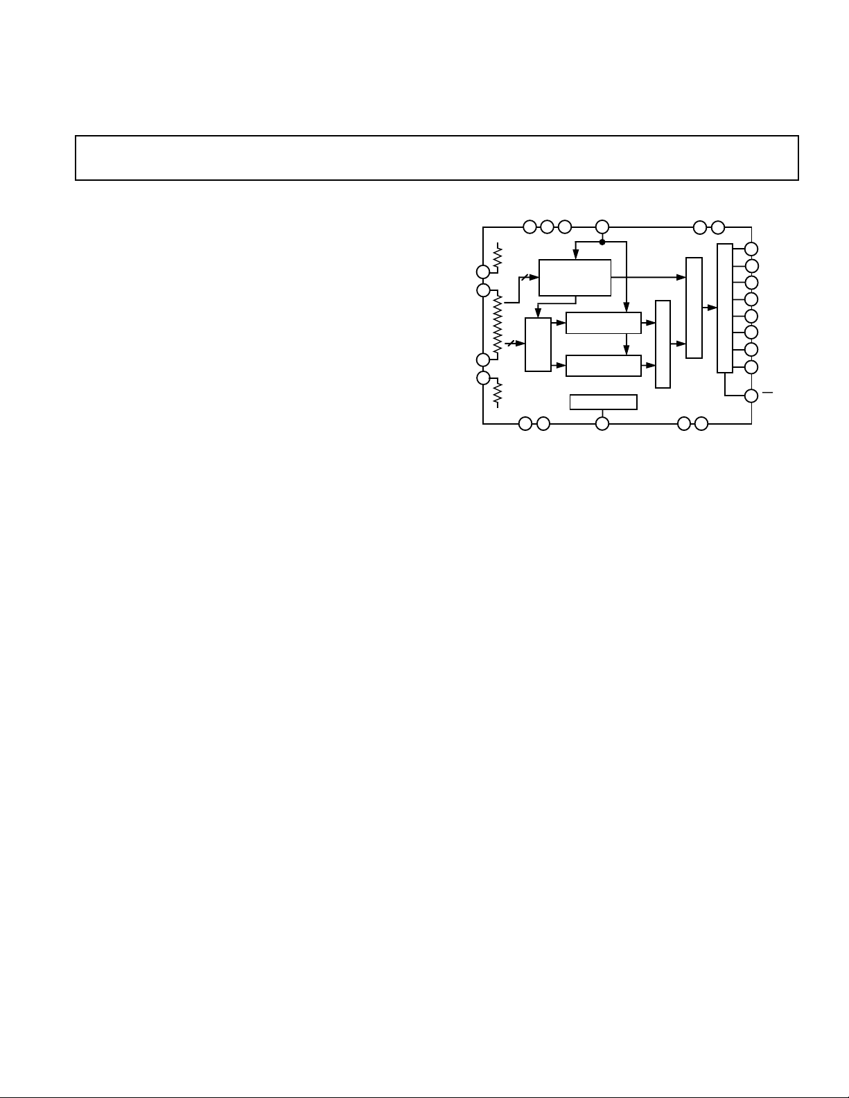
PRODUCT DESCRIPTION
The AD775 is a CMOS, low power, 8-bit, 20 MSPS sampling
analog-to-digital converter (ADC). The AD775 features a builtin sampling function and on-chip reference bias resistors to provide a complete 8-bit ADC solution. The AD775 utilizes a
pipelined/ping pong two-step flash architecture to provide high
sampling rates (up to 35 MHz) while maintaining very low
power consumption (60 mW).
Its combination of excellent DNL, fast sampling rate, low differential gain and phase errors, extremely low power dissipation,
and single +5 V supply operation make it ideally suited for a
variety of video and image acquisition applications, including
portable equipment. The AD775’s reference ladder may be connected in a variety of configurations to accommodate different
input ranges. The low input capacitance (11 pF typical) provides
an easy-to-drive input load compared to conventional flash
converters.
The AD775 is offered in both 300 mil SOIC and 400 mil DIP
plastic packages, and is designed to operate over an extended
commercial temperature range (–20°C to +75°C).
Sampling A/D Converter
AD775
FUNCTIONAL BLOCK DIAGRAM
PRODUCT HIGHLIGHTS
Low Power: The AD775 has a typical supply current of 12 mA,
for a power consumption of 60 mW. Reference ladder current
is also low: 6.6 mA typical, minimizing the reference power
consumption.
Complete Solution: The AD775’s switched capacitor design
features an inherent sample/hold function: no external SHA is
required. On-chip reference bias resistors are included to allow
a supply-based reference to be generated without any external
resistors.
Excellent Differential Nonlinearity: The AD775 features a
typical DNL of 0.3 LSBs, with a maximum limit of 0.5 LSBs.
No missing codes is guaranteed.
Single +5 V Supply Operation: The AD775 is designed to operate on a single +5 V supply, and the reference ladder may be
configured to accommodate analog inputs inclusive of ground.
Low Input Capacitance: The 11 pF input capacitance of the
AD775 can significantly decrease the cost and complexity of
input driving circuitry, compared with conventional 8-bit flash
ADCs.
REV. 0
Information furnished by Analog Devices is believed to be accurate and
reliable. However, no responsibility is assumed by Analog Devices for its
use, nor for any infringements of patents or other rights of third parties
which may result from its use. No license is granted by implication or
otherwise under any patent or patent rights of Analog Devices.
One Technology Way, P.O. Box 9106, Norwood, MA 02062-9106, U.S.A.
Tel: 617/329-4700 Fax: 617/326-8703
Page 2

(TA = +258C with AVDD, DVDD = +5 V, AVSS, DVSS = 0 V, VRT = 2.6 V, VRB = +0.6 V,
AD775–SPECIFICA TIONS
CLOCK = 20 MHz unless otherwise noted)
AD775J
Parameter Min Typ Max Units
RESOLUTION 8 Bits
DC ACCURACY
Integral Nonlinearity (INL) +0.5 1.3 LSB
Differential Nonlinearity (DNL) ±0.3 ± 0.5 LSB
No Missing Codes GUARANTEED
Offset
To Top of Ladder V
To Bottom of Ladder V
VIDEO ACCURACY
RT
RB
1
–10 –35 –60 mV
0 +15 +45 mV
Differential Gain Error 1.0 %
Differential Phase Error 0.5 Degrees
ANALOG INPUT
Input Range (V
) 2.0 V p-p
RT–VRB
Input Capacitance 11 pF
AC SPECIFICATIONS
2
Signal-to-Noise and Distortion (S/(N + D))
f
= 1 MHz 47 dB
IN
f
= 5 MHz 41 dB
IN
Total Harmonic Distortion (THD)
f
= 1 MHz –51 dB
IN
fIN = 5 MHz –42 dB
REFERENCE INPUT
Reference Input Resistance (R
Case 1: V
RT
= V
, VRB = V
RTS
) 230 300 450 Ω
REF
RBS
Reference Bottom Voltage (VRB) 0.60 0.64 0.68 V
Reference Span (V
Reference Ladder Current (I
Case 2: V
RT
= V
RTS
) 1.96 2.09 2.21 V
RT–VRB
, VRB = AV
) 4.4 7.0 9.6 mA
REF
SS
Reference Span (VRT–VRB) 2.25 2.39 2.53 V
Reference Ladder Current (I
) 5811 mA
REF
POWER SUPPLIES
Operating Voltages
AV
DV
DD
DD
+4.75 +5.25 Volts
+4.75 +5.25 Volts
Operating Current
IAV
DD
IDV
DD
IAVDD + IDV
DD
9.5 mA
2.5 mA
12 17 mA
POWER CONSUMPTION 60 85 mW
TEMPERATURE RANGE
Operating –20 +75 °C
NOTES
1
NSTC 40 IRE modulation ramp, CLOCK = 14.3 MSPS.
2
fIN amplitude = 0.3 dB full scale.
Specifications subject to change without notice. See Definition of Specifications for additional information.
–2–
REV. 0
Page 3
(TA = +258C with AVDD, DVDD = +5 V, AVSS, DVSS = 0 V, VRT = 2.6 V, VRB = +0.6 V,
DIGITAL SPECIFICATIONS
CLOCK = 20 MHz unless otherwise noted)
Parameter Symbol DV
LOGIC INPUT
High Level Input Voltage V
Low Level Input Voltage V
IH
IL
5.0 4.0 V
5.0 1.0 V
High Level Input Current
(V
= DVDD)I
IH
IH
5.25 5 µA
Low Level Input Current
(V
= 0 V) I
IL
Logic Input Capacitance C
IL
IN
5.25 –5 µA
LOGIC OUTPUTS
High Level Output Current
OE = DVSS, VOH = DVDD–0.5 V I
OE = DVDD, VOH = DV
DD
OH
I
OZ
4.75 –1.1 mA
5.25 16 µA
Low Level Output Current
OE = DVSS, VOL = 0.4 V I
OE = DVDD, VOL = 0 V I
OL
OZ
4.75 3.7 mA
5.25 16 µA
TIMING SPECIFICATIONS
Symbol Min Typ Max Units
DD
AD775
AD775J
Min Typ Max Units
5pF
Maximum Conversion Rate 20 35 MHz
Clock Period t
Clock High t
Clock Low t
Output Delay t
C
CH
CL
OD
50 ns
25 ns
25 ns
18 30 ns
Pipeline Delay (Latency) 2.5 Clock Cycles
Sampling Delay t
DS
4ns
Aperture Jitter 30 ps
Specifications subject to change without notice.
SAMPLE N+2
t
OD
VIN
CLK
OUT
t
DS
SAMPLE N+1
SAMPLE N
t
CH
t
CL
t
C
DATA N-3 DATA N-2 DATA N-1 DATA N
Figure 1. AD775 Timing Diagram
REV. 0
–3–
Page 4
AD775
WARNING!
ESD SENSITIVE DEVICE
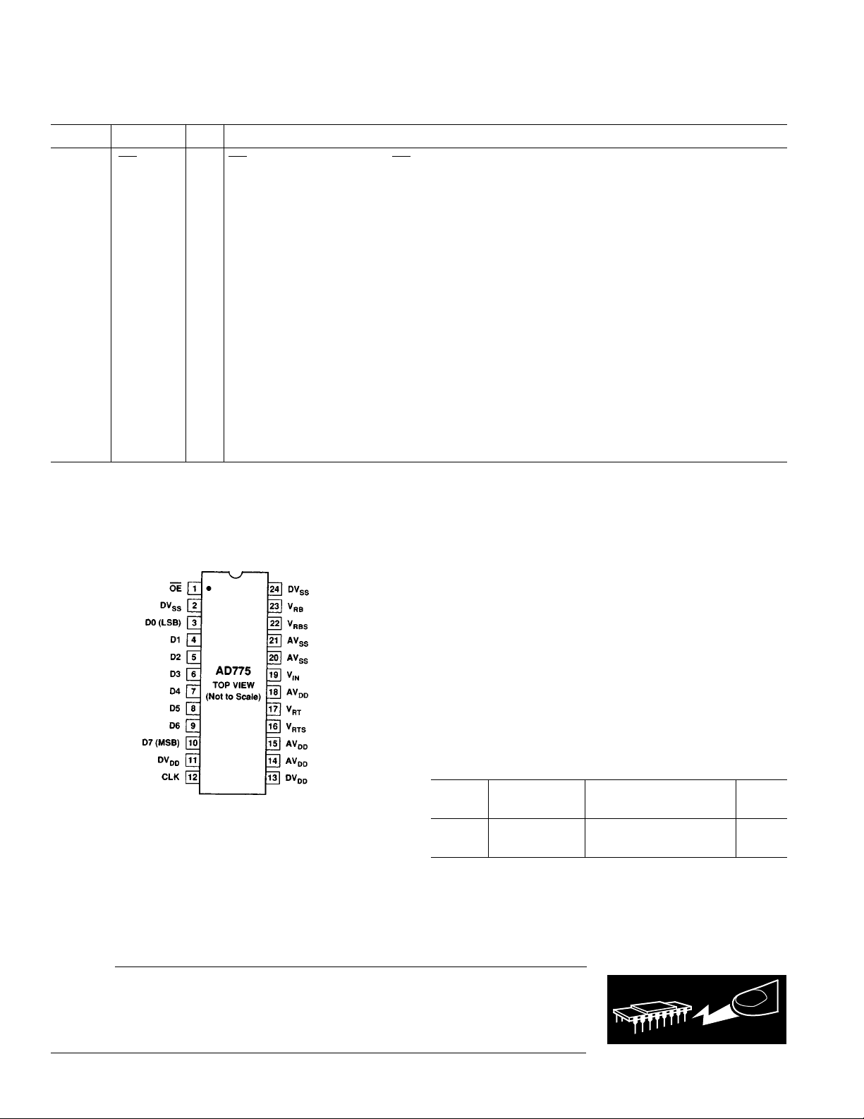
Pin No. Symbol Type Name and Function
PIN DESCRIPTION
1
OE DI OE = Low OE = High
Normal Operating Mode. High Impedance Outputs.
2, 24 DV
SS
P Digital Ground. Note: DVSS and AVSS pins should share a common ground plane on the circuit board.
3 D0 (LSB) DO Least Significant Bit, Data Bit 0.
4–9 D1–D6 DO Data Bits 1 Through 6.
10 D7 (MSB) DO Most Significant Bit, Data Bit 7.
11, 13 DV
DD
P +5 V Digital Supply. Note: DVDD and AVDD pins should share a common supply on the circuit board.
12 CLK DI Clock Input.
16 V
17 V
23 V
22 V
14, 15, 18 AV
RTS
RT
RB
RBS
DD
AI Reference Top Bias. Short to VRT for Self-Bias.
AI Reference Ladder Top.
AI Reference Ladder Bottom.
AI Reference Bottom Bias. Short to VRB for Self-Bias.
P +5 V Analog Supply. Note: DVDD and AVDD pins should share a common supply within 0.5 inches
of the AD775.
19 V
20, 21 AV
IN
SS
AI Analog Input. Input Span = VRT–VRB.
P Analog Ground. Note: DVSS and AVSS pins should share a common ground within 0.5 inches of the
AD775.
NOTE
Type: AI = Analog Input; DI = Digital Input; DO = Digital Output; P = Power.
PIN CONFIGURATION
(DIP and SOIC)
MAXIMUM RATINGS*
Supply Voltage (AVDD, DVDD) . . . . . . . . . . . . . . . . . . . . 7 V
Supply Difference (AV
Ground Difference (AV
Reference Voltage (V
Analog Input Voltage (VIN) . . . . . . . . . . . . . . . . . . VDD to V
Digital Input Voltage (CLK) . . . . . . . . . . . . . . . . . VDD to V
Digital Output Voltage (VOH, VOL) . . . . . . . . . . . . VDD to V
–DVDD) . . . . . . . . . . . . . . . . . . 0 V
DD
–DVSS) . . . . . . . . . . . . . . . . . . . 0 V
SS
, VRB) . . . . . . . . . . . . . . . . VDD to V
RT
SS
SS
SS
SS
Storage Temperature . . . . . . . . . . . . . . . . . . –55°C to +150°C
*Stresses above those listed under “Absolute Maximum Ratings” may cause
permanent damage to the device. This is a stress rating only and functional
operation of the device at these or any other conditions above those indicated in the
operational sections of this specification is not implied. Exposure to absolute
maximum rating conditions for extended periods may affect device reliability.
Temperature Package Package
Model Range Description Option
AD775JN –20°C to +75°C 24-Pin 400 Mil Plastic DIP N-24B
AD775JR –20°C to +75°C 24-Pin 300 Mil SOIC R-24A
CAUTION
ESD (electrostatic discharge) sensitive device. Electrostatic charges as high as 4000 V readily
accumulate on the human body and test equipment and can discharge without detection.
Although the AD775 features proprietary ESD protection circuitry, permanent damage may
occur on devices subjected to high energy electrostatic discharges. Therefore, proper ESD
precautions are recommended to avoid performance degradation or loss of functionality.
–4–
ORDERING GUIDE
REV. 0
Page 5

–30
–54
0.1 1 10
–36
–42
–48
f
IN
– MHz
THD – dB
+1
–1
+FULLSCALE–FULLSCALE
0
INL – LSB
54
48
42
36
30
24
S/(N + D) – dB
18
12
6
0
0.1 1 10
fIN – MHz
Figure 2. S/(N + D) vs. Input Frequency at 20 MSPS Clock
Rate (V
= –0.3 dB)
IN
AD775
Figure 5. THD vs. Input Frequency at 20 MSPS Clock Rate
= –0.3 dB)
(V
IN
0
–10
–20
–30
–40
–50
dB
–60
–70
–80
–90
–100
1.0
0
FREQUENCY – MHz
10.0
9.08.07.06.05.04.03.02.0
Figure 3. Typical FFT at 1 MHz Input, 20 MSPS Clock Rate
= –0.5 dB)
(V
IN
+0.4
+0.3
+0.2
+0.1
0
–10
–20
–30
–40
–50
dB
–60
–70
–80
–90
–100
1.0
0
FREQUENCY – MHz
10.0
9.08.07.06.05.04.03.02.0
Figure 6. Typical FFT at 5 MHz Input, 20 MSPS Clock Rate
(V
= –0.5 dB)
IN
0
DNL – LSB
–0.1
–0.2
–0.3
–0.4
–FULLSCALE
Figure 4. Typical Differential Nonlinearity (DNL)
REV. 0
+FULLSCALE
Figure 7. Typical Integral Nonlinearity (INL)
–5–
Page 6

AD775
16
23
17
22
AV
DD
AV
SS
325Ω
90Ω
300Ω
AD775
*VALUES FOR
RESISTANCE
ARE TYPICAL
0.1µF
0.1µF
DEFINITIONS OF SPECIFICATIONS
Integral Nonlinearity (INL)
Integral nonlinearity refers to the deviation of each individual
code from a line drawn from “zero” through “full scale.” The
point used as “zero” occurs 1/2 LSB before the first code transition. “Full scale” is defined as a level 1 1/2 LSB beyond the
last code transition. The deviation is measured from the center
of each particular code to the true straight line.
Differential Nonlinearity (DNL, No Missing Codes)
An ideal ADC exhibits code transitions that are exactly 1 LSB
apart. DNL is the deviation from this ideal value. It is often
specified in terms of the resolution for which no missing codes
(NMC) is guaranteed.
Offset Error
The first code transition should occur at a level 1/2 LSB above
nominal negative full scale. Offset referred to the Bottom of
Ladder V
is defined as the deviation from this ideal. The last
RB
code transition should occur 1 1/2 LSB below the nominal
positive full scale. Offset referred to the Top of Ladder V
RT
is
defined as the deviation from this ideal.
Differential Gain
The percentage difference between the output amplitudes of a
small high frequency sine wave at two stated levels of a low frequency signal on which it is superimposed.
Differential Phase
The difference in the output phase of a small high frequency
sine wave at two stated levels of a low frequency signal on which
it is superimposed.
Pipeline Delay (Latency)
The number of clock cycles between conversion initiation and
the associated output data being made available. New output
data is provided every clock cycle.
Signal-to-Noise Plus Distortion Ratio (S/N+D)
S/N+D is the ratio of the rms value of the measured input signal
to the rms sum of all other spectral components including harmonics but excluding dc. The value for S/N+D is expressed in
decibels.
Total Harmonic Distortion (THD)
THD is the ratio of the rms sum of the first six harmonic components to the rms value of the measured input signal and is expressed as a percentage or in decibels.
THEORY OF OPERATION
The AD775 uses a pipelined two-step (subranging) flash architecture to achieve significantly lower power and lower input
capacitance than conventional full flash converters while still
maintaining high throughput. The analog input is sampled by
the switched capacitor comparators on the falling edge of the
input clock: no external sample and hold is required. The coarse
comparators determine the top four bits (MSBs), and select the
appropriate reference ladder taps for the fine comparators. With
the next falling edge of the clock, the fine comparators determine
the bottom four bits (LSBs). Since the LSB comparators require
a full clock cycle between their sampling instant and their decision, the converter alternates between two sets of fine comparators in a “ping-pong” fashion. This multiplexing allows a new
input sample to be taken on every falling clock edge, thereby
providing 20 MSPS operation. The data is accumulated in the
correction logic and output through a three-state output latch
on the rising edge of the clock. The latency between input sampling and the corresponding converted output is 2.5 clock cycles.
All three comparator banks utilize the same resistive ladder for
their reference input. The analog input range is determined by
the voltages applied to the bottom and top of the ladder, and
the AD775 can digitize inputs down to 0 V using a single supply. On-chip application resistors are provided to allow the
ladder to be conveniently biased by the supply voltage.
The AD775 uses switched capacitor autozeroing techniques to
cancel the comparators’ offsets and achieve excellent differential
nonlinearity performance: typically ± 0.3 LSB. The integral
nonlinearity is determined by the linearity of the reference ladder and is typically +0.5 LSB.
APPLYING THE AD775
REFERENCE INPUT
The AD775 features a resistive reference ladder similar to that
found in most conventional flash converters. The analog input
range of the converter falls between the top (V
(V
) voltages of this ladder. The nominal resistance of the lad-
RB
) and bottom
RT
der is 300 ohms, though this may vary from 230 ohms to 450
ohms. The minimum recommended voltage for V
is 0 V; the
RB
linearity performance of the converter may deteriorate for input
spans (V
maximum ladder top voltage (V
as high as the positive supply voltage (AV
) below 1.8 V. While 2.8 V is the recommended
RB–VRB
), the top of the ladder may be
RT
) with minimal lin-
DD
earity degradation.
Figure 8. Reference Configuration: 0.64 V to 2.73 V
To simplify biasing of the AD775, on-chip reference bias resistors are provided on Pins 16 and 22. The two recommended
configurations for these resistors are shown in Figures 8 and 9.
–6–
REV. 0
Page 7

In the topology shown in Figure 8, the top of the ladder (VRT)
16
22
17
23
AD775
NC
NC
NC = NO CONNECT
0.1µF
V
RTS
V
RT
V
RBS
V
RB
1
3
2
AD822
500pF
10kΩ
20Ω
10kΩ
0.1µF
7
5
6
AD822
500pF
10kΩ
20Ω
10kΩ
0.1µF
422Ω
140Ω
422Ω
1
3
2V
OUT
GND
V
IN
AD680
0.1µF
+5V
is shorted to the top bias resistor (V
16), while the bottom of the ladder (V
tom bias resistor (V
) (Pin 23 shorted to Pin 22). This creates
RBS
a resistive path (nominally 725 ohms) between AV
) (Pin 17 shorted to Pin
RTS
) is shorted to the bot-
RB
and AVSS.
DD
For nominal supply voltages (5 V and 0 V respectively), this
creates an input range of 0.64 V to 2.73 V.
Both top and bottom of the reference ladder should be decoupled, preferably with a chip capacitor to ground to minimize
reference noise.
The topology shown in Figure 9 provides a ground-inclusive
input range. The bottom of the ladder (V
(0 V), while the top of the ladder (V
board bias resistor (V
of 0 V to +2.4 V for AV
floating, or shorted to AV
). This provides a nominal input range
RTS
of 5 V. The V
DD
.
SS
) is shorted to AVSS.
RB
) is connected to the on-
RT
pin may be left
RBS
AD775
Figure 11. Reference Configuration: 0.7 V to 3.2 V
ANALOG INPUT
The impedance looking into the analog input is essentially
capacitive, as shown in the equivalent circuit of Figure 12, typically totalling around 11 pF. A portion of this capacitance is
parasitic; the remainder is part of the switched capacitor struc-
0.1µF
AV
DD
325Ω
16
17
AD775
ture of the comparator arrays. The switches close on the rising
300Ω
90Ω
AV
SS
*VALUES FOR
RESISTANCE
ARE TYPICAL
AV
SS
23
22
Figure 9. Reference Configuration: 0 V to +2.4 V
edge of the clock, acquire the input voltage, and open on the
clock’s falling edge (the sampling instant). The charge that must
be moved onto the capacitors during acquisition will be a function of the converter’s previous two samples, but there should be
no sample-to-sample crosstalk so long as ample driving impedance and acquisition time are provided.
SWITCHES EACH
AV
DD
CLOCK CYCLE
More elaborate topologies can be used for those wishing to
provide an input span based on an external reference voltage.
C2
The circuit in Figure 10 uses the AD780 2.5 V reference to
drive the top of the ladder (V
ladder grounded to provide an input span of 0 V to +2.5 V. This is
modified in Figure 11 to shift the 2.5 V span up 700 mV.
+5V
AD780
1
NC
2
3
NC
0.1µF
4
), with the bottom (VRB) of the
RT
8
NC
16
7
NC
6
NC
5
NC
0.1µF
17
AD775
V
IN
AV
C1
SS
C1 + C2 + C3 ≈ 11pF
SWITCHES ON ALTERNATE
CLOCK CYCLES
C3
AD775
Figure 12. Equivalent Analog Input Circuit (VIN)
For example, to ensure accurate acquisition (to 1/4 bit accuracy)
of a full-scale input step in less than 20 ns, a source impedance
22
NC
23
NC = NO CONNECT
Figure 10. Reference Configuration: 0 V to 2.5 V
The AD775 can accommodate dynamic changes in the reference
voltage for gain or offset adjustment. However, conversions that
are in progress, including those in the converter pipeline, while
the reference voltages are changing will be invalid.
REV. 0
of less than 100 ohms is recommended. Figure 13 shows one
option of input buffer circuitry using the AD817. The AD817
acts as both an inverting buffer and level shifting circuit. In
order to level shift the ground-based input signal to the dc level
required by the input of the AD775, the supply voltage is resistively divided to produce the appropriate voltage at the noninverting input of the AD817. For most applications, the AD817
provides a low cost, high performance level shifter. The AD811
is recommended for systems which require faster settling times.
–7–
Page 8

AD775
0V
+5V
1kΩ
100
1kΩ
DC
5.6kΩ
AD817
1.5V
AD775
DC
A
19
IN
90
80
10µF
1kΩ
Figure 13. Level Shifting Input Buffer
The analog input range is set by the voltage at the top and bottom of the reference ladder. In general, the larger the span
(V
), the better the differential nonlinearity (DNL) of the
RT–VRB
converter; a 1.8 V span is suggested as a minimum to realize
good linearity performance. AS the input voltage exceeds 2.8 V
(for AV
= 4.75 V), the input circuitry may start to slightly
DD
degrade the acquisition performance.
CLOCK INPUT
The AD775’s internal control circuitry makes use of both clock
edges to generate on-chip timing signals. To ensure proper
settling and linearity performance, both t
and tCL times
CH
should be 25 ns or greater. For sampling frequencies at or near
20 MSPS, a 50% duty cycle clock is recommended. For slower
sampling applications, the AD775 can accommodate a wider
range of duty cycles, provided each clock phase is as least 25 ns.
Under certain conditions, the AD775 can be operated at sampling rates above 20 MSPS. Figure 14 shows the signal-to-noise
plus distortion (S/(N+D)) performance of a typical AD775
versus clock frequency. It is extremely important to note that the
maximum clock rate will be a strong function of both temperature and
supply voltage. In general, the part slows down with increasing
temperature and decreasing supply voltage.
50
40
30
20
S(N + D) – dB
70
60
50
POWER DISSIPATION – mW
40
30
0
10
CLOCK FREQUENCY – MHz
20
30
40
Figure 15. Power Dissipation vs. Clock Frequency
In applications sensitive to aperture jitter, the clock signal
should have a fall time of less than 3 ns. High speed CMOS
logic families (HC/HCT) are recommended for their symmetrical swing and fast rise/fall times. Care should be taken to minimize the fanout and capacitive loading of the clock input line.
DIGITAL INPUTS AND OUTPUTS
The AD775’s digital interface uses standard CMOS, with logic
thresholds roughly midway between the supplies (DV
, DVDD).
SS
The digital output is presented in straight binary format, with
full scale (1111 1111) corresponding to V
(0000 0000) corresponding to V
= VRB. Excessive capacitive
IN
= VRT, and zero
IN
loading of the digital output lines will increase the dynamic
power dissipation as well as the on-chip digital noise. Logic
fanout and parasitic capacitance on these lines should be minimized for optimum noise performance.
The data output lines may be placed in a high output impedance
state by bringing
typical timing for access and float delay times (t
OE (Pin 1) to a logic high. Figure 16 indicates
and t
HL
DD
respectively). Note that even when the outputs are in a high
impedance state, activity on the digital bus can couple back to
the sensitive analog portions of the AD775 and corrupt conversions in progress.
OE
t
DD
t
HL
10
0
0.1 1 10010
CLOCK FREQUENCY – MHz
Figure 14. S(N + D) vs. Clock Frequency (Temperature
°
C)
= +25
A significant portion of the AD775’s power dissipation is proportional to the clock frequency: Figure 15 illustrates this
tradeoff for a typical part.
–8–
DATA
OUTPUT
THREE-STATE
(HIGH IMPEDANCE)
t
= 18ns TYPICAL
DD
DATA ACTIVE
t
= 12ns TYPICAL
HL
Figure 16. High Impedance Output Timing
REV. 0
Page 9

AD775
J6
C15
D
C13
A
J3
TP4
V
RT
C12
+5V
D
C18
+5VA
J9
J5
C14
J4
TP3
VRB
3
2
1
AD822
C4
390pF
R10
20
1/2 U2
R9
10k
8
C9
A
+5VA
6
AD822
7
C3
390pF
R5
20
1/2 U2
R6
10k
J2
5
4
A
A
R7
10k
A
A
9
3
4
5
1
2
6
7
8
10
G1
A1
A2
A3
A4
A5
A6
A7
A8
GND
74ALS541
12
18
17
16
20
19
15
14
13
11
D
D
C22
+5V
V
CC
G2
Y1
Y2
Y3
Y4
Y5
Y6
Y7
Y8
TP13
ENABLE
J10
D
D
D
1
40
D
P2-40 PIN IDC
A
R8
10k
D
3
2
U1
VINV
OUT
GND
AD680
1
A
+5VA
A
C2
R3
499
C1
A
R2
500
R1
500
R11
75
R12
4.99k
3
2
6
AD817
U3
7
C6
A
C8
22µF
R13
20
Q1
2N3904
TP2
R4
49.9
A
TP1
J1
ANALOG
INPUT
4
C5
V
EE
V
CC
V
EE
A
V
CC
R14
500
+5VA
R15
499
CR1
1N4148
+5VA
A
C7
10pF
TP5
V
IN
TP10
R16
49.9
D
TP9
J8
CLOCK
( )
56
1/6
U7
98
1/6
U7
13
14
17
18
19
15
16
20
21
22
23
24
2
12
11
8
7
6
10
9
5
4
3
1
DV
SS
D2
D3
D4
D0
D1
D5
D6
D7
DV
DD
CLK
OE
V
RB
AV
SS
V
IN
AV
DD
AV
SS
V
RT
V
RTS
AV
DD
AV
DD
DV
DD
DV
SS
V
RBS
AD775
= 47µF ELECTROLYTIC CAPACITOR
UNLESS OTHERWISE NOTED
= 0.1µF CERAMIC CAPACITOR
UNLESS OTHERWISE NOTED
NOTES
VINV
OUT
GND
U4
78M05
J7
C11
D
C21
TP12
TP6
+5V
+5VA
A
V
CC
C16
C20
C19
TP7
TP8
TP11
V
CC
V
EE
1
2
3
4
5
6
V
U5
U6
POWER SUPPLY CONNECTIONS AND DECOUPLING
The analog and digital supplies of the AD775 have been separate to prevent the typically large transients associated with the
on-chip digital circuitry from coupling into the analog supplies
(AV
, AVSS). However, in order to avoid possible latch-up
DD
conditions, AV
and DVDD must share a common supply
DD
external to the part, preferably a common source somewhere on
the PC board.
Each supply should be decoupled by a 0.1 µF capacitor located
as close to the device pin as possible. Surface-mount capacitors,
by virtue of their low parasitic inductance, are preferable to
through-hole types. A larger capacitor (10 µF electrolytic)
should be located somewhere on the board to help decouple
large, low frequency supply noise. For specific layout information, refer to the AD775 Evaluation Board section of the data
sheet.
Figure 17. AD775 Evaluation Board Schematic
REV. 0
APPLICATIONS
AD775 EVALUATION BOARD
Figures 17 through 22 show the schematic and printed circuit
board (PCB) layout for the AD775 evaluation board. Referring
to Figure 17, the input signal is buffered by U3, an AD817 op
amp configured as a unity-gain follower. The signal is then accoupled and dc-biased by adjusting potentiometer R14. Video
and imaging applications would typically use a dc-restoration
circuit instead of the manual potentiometer adjustment. Q1, an
emitter-follower, buffers the input signal and provides ample
current to drive a simple low-pass filter. The filtering is included
to limit wideband noise and highlight the fact that the AD775
can be driven from a nonzero source impedance.
The reference circuit is similar to the one shown in Figure 11
with the exception that R1 and R2 allow precise adjustment of
–9–
Page 10

AD775
VRT and VRB. Note that the VRT and VRB traces (see Figures 19
and 20) are run in parallel and in the same proximity. Any noise
coupling is likely to be common mode to both signals and would
result in an offset error but not a gain error. The entire reference
circuit is powered by a single +5 V supply. The minimum voltage for V
is determined by the impedance of the AD822 out-
RB
put stage and the amount of current flowing through the
internal resistor ladder of the AD775.
The sampling clock is buffered by U7, a 74HC04 inverter. It is
recommended that the output loading of the inverter is minimized in order to maintain fast transition times on the clock. An
additional inverter is used to provide a buffered clock signal
whose rising edges indicate that data is valid. A 74ALS541
buffers the eight digital data outputs of the AD775 to improve
the load driving capability.
The multilayer PCB board layout shows some of the important
design guidelines recommended for the AD775. The most im-
Table I. Components List
Reference Designator Description Quantity
R1, R2, R14 Potentiometer 3
R3, R15 Resistor, 1%, 499 Ω 2
R4, R13, R16 Resistor, 1%, 49.9 Ω 3
R5, R10 Resistor, 1%, 20 Ω 2
R6–R9 Resistor, 1%, 10 kΩ 4
R11 Resistor, 1%, 75 Ω 1
R12 Resistor, 1%, 4.99 kΩ 1
CR1 Diode, 1N4148 1
C1, C2, C5, C6, C9, C12–C15, C18
C20, C22, C23 Ceramic Cap, Z5U, 0.1 µF13
C3, C4 Capacitor, Mica, 390 pF 2
C7 Capacitor, Mica, 10 pF 1
C8 Capacitor, Tantalum, 22 µF, 16 V 1
C11, C16, C19, C21 Capacitor, Alum. Electrolytic, 47 µF, 16 V 4
Q1 Transistor, 2N3904 1
U1 AD680JT 1
U2 AD822AN 1
U3 AD817AN 1
U4 78M05 1
U5 AD775 1
U6 74ALS541N 1
U7 74HC04N 1
J1, J8 BNC Jack 2
portant aspect is the power and ground distribution. While the
AD775 has separate analog and digital power and ground pins,
the AD775 should be treated as an entirely analog component.
The ground plane is joined close to the ADC in order to maintain a low potential difference across the analog and digital
ground pins. Because the power and grounds are derived from a
common point, a slit in the ground plane is used to minimize
any interaction between the analog and digital return currents.
The power for the AD775, AV
the same supply. Separate traces are run to AV
and DVDD, are derived from
DD
and DV
DD
DD
and joined together at the source. While not used on the evaluation board, a ferrite bead or inductor can effectively isolate noise
generated by digital circuitry such as the output buffers. In cases
where only a single supply is available, the inductor should not
be placed between AV
and DVDD. Instead, both supplies of
DD
the AD775 should be connected together and isolated from
entirely digital components.
–10–
REV. 0
Page 11

AD775
Figure 18. Silkscreen Layer (Not to Scale)
Figure 20. Solder Side PCB Layout (Not to Scale)
Figure 19. Component Side PCB Layout (Not to Scale)
REV. 0
Figure 21. Ground Plane PCB Layout (Not to Scale)
–11–
Page 12

AD775
PIN 1
13
24
12
1
0.221 (5.6)
0.205 (5.2)
0.327 (8.3)
0.295 (7.5)
0.022 (0.55)
0.014 (0.35)
0.050 (1.27)
BSC
0.606 (15.4)
0.586 (14.9)
0.089 (2.25)
0.067 (1.70)
0.012 (0.12)
0.002 (0.05)
0.012 (0.30)
0.006 (0.15)
0.028 (0.7)
0.012 (0.3)
0.272 (6.9)
C1830–18–8/93
PIN 1
0.200 (5.05)
0.125 (3.18)
0.118 (3.00)
24
MIN
0.024 (0.60)
0.016 (0.40)
Figure 22. Power Plane PCB Layout (Not to Scale)
OUTLINE DIMENSIONS
Dimensions shown in inches and (mm).
Plastic DIP (N-24B)
13
0.346 (8.80)
0.330 (8.40)
0.053 (1.35)
0.041 (1.05)
12
0.020
(0.50)
MIN
SEATING
PLANE
0.400 (10.16)
15
°
0.014 (0.35)
0
°
0.008 (0.20)
0.195 (4.95)
0.125 (3.18)
1
1.205 (30.60)
1.185 (30.10)
0.100
(2.54)
BSC
SOIC (R-24A)
PRINTED IN U.S.A.
–12–
REV. 0
 Loading...