

Page 1
24-bit Capacitance to Digital Converter
Preliminary Technical Data
FEATURES
Capacitance to Digital Converter (CDC)
Standard One Chip Solution
Interfaces to Single or Differential Floating Sensors
Resolution: 20 aF (i.e. 19-bit) at 16.6 Hz
Accuracy: 2 fF
Linearity: 0.01%
Input Range: ±4 pF
Offset / Common Capacitance Removal: up to 17 pF
Update rate: 5 Hz to 90 Hz
Simultaneous 50 Hz and 60 Hz rejection at 16.6 Hz
Tolerant of ground capacitance and ground leakage
current
Temperature sensor on chip
Resolution: 0.1°C, accuracy: ±2°C
Voltage input channel
Internal clock oscillator
2
2-Wire Serial Interface (I
C®-Compatible)
Power
2.7 V to 5.25 V Single-Supply Operation
1 mA Current Consumption
Operating temperature: -40°C to +125°C
Package: 16-lead TSSOP
APPLICATIONS
Automotive, Industrial and Medical Systems for:
Pressure Measurement
Position Sensors
Level Sensors
Flowmeters
Humidity Sensors
Impurity Detection
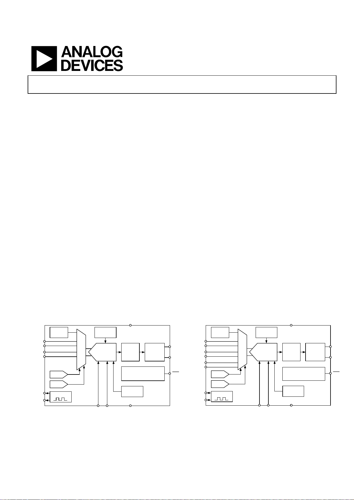
FUNCTIONAL BLOCK DIAGRAMS
V
VIN(+)
VIN(
C
C
IN1
IN1
EXCA
EXCB
TEMP
SENSOR
-
)
(+)
(
-
)
CAP DAC
CAP DAC
EXCITATION
MUX
CLOCK
GENERATOR
24-BITΣ-
MODULATOR
∆
Figure 1. Figure 2.
DD
AD7745
DIGITAL
FILTER
CONTROL LOGIC
CALIBRATION
VOLTAGE
REFERENCE
GNDREFIN(+) REFIN(-)
I2C
SERIAL
INTERFACE
SDA
SCL
RDY
with Temperature Sensor
AD7745/AD7746
GENERAL DESCRIPTION
The AD7745/AD7746 is a high-resolution Σ−∆ capacitance to
digital converter (CDC). The capacitance to be measured is
connected directly to the device inputs. The architecture
features inherent high resolution (24-bit no missing codes,
19-bit effective resolution at 16.6 Hz data rate), high linearity
(±0.01%) and high accuracy (±2 fF factory calibrated).
The AD7745/AD7746 capacitance input range is ±4 pF
(changing), while it can accept up to 17 pF absolute capacitance
(not changing), which is compensated by an on-chip digital to
capacitance converter (CAPDAC).
The AD7745 has one capacitance input channel, while the
AD7746 has two channels. Each channel can be configured as
single ended or differential. The AD7745/AD7746 is designed
for floating capacitive sensors. For capacitive sensors with one
plate connected to ground, the AD7747 is recommended.
The parts have an on-chip temperature sensor with resolution
of 0.1°C and accuracy of ±2°C. The on-chip voltage reference
and the on-chip clock generator eliminate the need for any
external components in most capacitive sensor applications.
The parts have a standard voltage input, which together with the
differential reference input allows easy interface to an external
temperature sensor, such as an RTD, thermistor or diode.
The AD7745/AD7746 has a 2-wire, I
interface. Both parts operate from a single 3 V or 5 V power
supply. They are specified over the automotive temperature
range of -40°C to +125°C and are housed in a 16-lead TSSOP
package.
CLOCK
GENERATOR
24-BITΣ-
MODULATOR
REFIN(+) REFIN(
C
C
C
C
VIN(+)
VIN(
IN1
IN1
IN2
IN2
EXC1
EXC2
TEMP
SENSOR
-
)
(+)
(
-
)
(+)
(
-
)
CAP DAC
CAP DAC
EXCITATION
MUX
2
C compatible serial
V
DD
AD7746
∆
DIGITAL
FILTER
CONTROL LOGIC
CALIBRATION
VOLTAGE
REFERENCE
-
)
GND
GND
I2C
SERIAL
INTERFACE
SDA
SCL
RDY
Rev. PrF, 3. March 2005
Information furnished by Analog Devices is believed to be accurate and reliable.
However, no responsibility is assumed by Analog Devices for its use, nor for any
infringements of patents or other rights of third parties that may result from its use.
Specifications subject to change without notice. No license is granted by implication
or otherwise under any patent or patent rights of Analog Devices. Trademarks and
registered trademar ks are the property of their respective companies.
One Technology Way, P.O. Box 9106, Norwood, MA 02062-9106, U.S.A.
Tel: 781.329.4700
Fax: 781.326.8703 © 2005 Analog Devices, Inc. All rights reserved.
www.analog.com
Page 2

AD7745/AD7746
TABLE OF CONTENTS
AD7745/AD7746—PRELIMINARY SPECIFICATIONS........... 3
Timing Specifications....................................................................... 5
Absolute Maximum Ratings............................................................ 5
Output Noise and Resolution SpecificationS................................ 6
Pin Configuration and Function Descriptions............................. 7
SERIAL INTERFACE....................................................................... 8
Write Operation............................................................................ 8
Read Operation............................................................................. 8
General Call................................................................................... 9
AD7745/AD7746 Reset ............................................................... 9
REGISTER DESCRIPTIONS........................................................ 10
Status Register............................................................................. 11
Cap Data Register....................................................................... 11
VT Data Register ........................................................................11
Cap Setup Register ..................................................................... 12
VT Setup Register....................................................................... 12
Exc Setup Register ...................................................................... 13
Configuration Register .............................................................. 14
Cap DAC A Register................................................................... 15
Cap DAC B Register................................................................... 15
Cap Offset Register..................................................................... 15
Cap Gain Register....................................................................... 15
Volt Gain Register....................................................................... 15
Typical Application Diagram ........................................................ 16
Outline Dimensions....................................................................... 17
ESD Caution................................................................................ 17
Preliminary Technical Data
Rev. PrF | Page 2 of 17
Page 3

Preliminary Technical Data
AD7745/AD7746
AD7745/AD7746—PRELIMINARY SPECIFICATIONS
Table 1. (VDD = 2.7 V to 3.3 V, or 4.75V to 5.25V, GND = 0 V, –40°C to +125°C, unless otherwise noted.)
Parameter Min Typ Max Unit Test Conditions/Comments
CAPACITIVE INPUT (INPUTS)
Conversion Input Range ±4.096 pF Factory calibrated
Integral Nonlinearity (INL) 1 ±0.01 % of FSR
No-missing Codes 1 24 bit 62ms conversion time
Resolution p-p 16.5 bit 62ms conversion time
Resolution effective 19 bit 62ms conversion time
Output Noise rms 5
Absolute Error 2 ±2 fF 25°C, after offset calibration
Offset Error 32 aF After system offset calibration
Offset Drift vs. Temperature -1 aF/°C
Gain Error 0.02 % of FS
Gain Drift vs. Temperature 1 -29 -27 -25 ppm of FS/°C
Allowed Capacitance to GND 1 60 pF
Power Supply Rejection 500 aF/V
Conversion Time 11.0 217.3 ms Configurable via digital interface
CAPDAC
Full Range 17 21 pF
Resolution 3 164 fF 7-bit CAPDAC
Drift vs. Temperature 1 +27 ppm of FS/°C
EXCITATION
Frequency 32 kHz Exc. setup register bit CLKCTRL = 0
Voltage across Capacitance ± VDD /8 V Configurable via digital interface
± VDD /4 V
± VDD /2 V
Average DC Voltage across Capac. < ±50 mV
Allowed Capacitance to GND 1 100 pF
TEMPERATURE SENSOR 4
Resolution 0.1 °C
Error 1 ±0.5 ±2 °C Internal temperature sensor
±2 ±4 °C External sensing diode
VOLTAGE INPUT 4
Differential VIN Voltage Range ±V
Absolute VIN Voltage GND –0.03 VDD +0.03 V
Integral Nonlinearity (INL) 1 ±5 ±15 ppm of FSR
No-missing Codes 1 24 Bit 62ms conversion time
Resolution p-p 16 bits 62ms conversion time
Output Noise 3 µV rms 62ms conversion time
Offset Error ±3 µV
Offset Drift vs. Temperature 15 nV/°C
Full-Scale Error 5 TBD µV
Full-Scale Drift vs. Temperature 0.5 ppm of FSR/°C External reference
Average VIN Input Current 400 nA/V
Analog VIN Input Current Drift ±50 pA/V/°C
Power Supply Rejection 90 dB External reference
Power Supply Rejection 80 dB Internal reference
Common-Mode Rejection 90 dB
Conversion Time 20.1 122.1 ms Configurable via Digital Interface
± V
× 3/8
DD
V
REF
V
aF/√Hz
62ms conversion time
62ms conversion time
Rev. PrF | Page 3 of 17
Page 4

AD7745/AD7746
Preliminary Technical Data
Parameter Min Typ Max Unit Test Conditions/Comments
INTERNAL VOLTAGE REFERENCE
Voltage 1.168 1.17 1.172 V At VDD = 4V, TA = 25°C
Drift vs. Temperature 10 ppm/°C
EXTERNAL VOLTAGE REFERENCE INPUT
Differential REFIN Voltage 1 0.1 2.5 VDD V
Absolute REFIN Voltage GND –0.03 VDD +0.03 V
Average REFIN Input Current 400 nA/V
Average REFIN Input Current Drift ±50 pA/V/°C
SERIAL INTERFACE
LOGIC INPUTS (SCL, SDA)
VIH Input High Voltage 2.1 V
VIL Input Low Voltage 0.8 V
Hysteresis 150 mV
OPEN-DRAIN OUTPUT (SDA)
VOL Output Low Voltage 0.4 V
IOH Output High Leakage Current 0.1 1 µA V
LOGIC OUTPUT (
RDY
)
VOL Output Low Voltage 0.4 V I
VOH Output High Voltage 4.0 V I
VOL Output Low Voltage 0.4 V I
VOH Output High Voltage DVDD – 0.6 V I
I
= −6.0 mA
SINK
= VDD
OUT
= 1.6 mA, VDD = 5 V
SINK
= 200 µA, VDD = 5 V
SOURCE
= 100 µA, VDD = 3 V
SINK
= 100 µA, VDD = 3 V
SOURCE
POWER REQUIREMENTS
VDD to GND Voltage 4.75 5.25 V VDD = 5 V nominal
2.7 3.3 V VDD = 3 V nominal
IDD Current 1 mA Digital inputs equal to VDD or GND
IDD Current Power Down Mode 1 µA Digital inputs equal to VDD or GND
1
Specification is not production tested, but is supported by characterization data at initial product release.
2
Factory calibrated The absolute error includes factory gain calibration error, integral nonlinearity error, and offset error after system offset calibration, all at 25°C.
At different temperatures, compensation for gain drift over temperature is required.
3
The CAPDAC resolution is 7-bit in the actual CAPDAC full range. Using the on-chip offset calibration or adjusting the capacitive offset calibration register can further
reduce the CIN offset or the non-changing CIN component.
4
The VTCHOP bit in the VT SETUP register must be set to 1 for the specified temperature sensor and voltage input performance.
5
Full-scale error applies to both positive and negative full-scale.
Rev. PrF | Page 4 of 17
Page 5
Preliminary Technical Data
A
AD7745/AD7746
TIMING SPECIFICATIONS
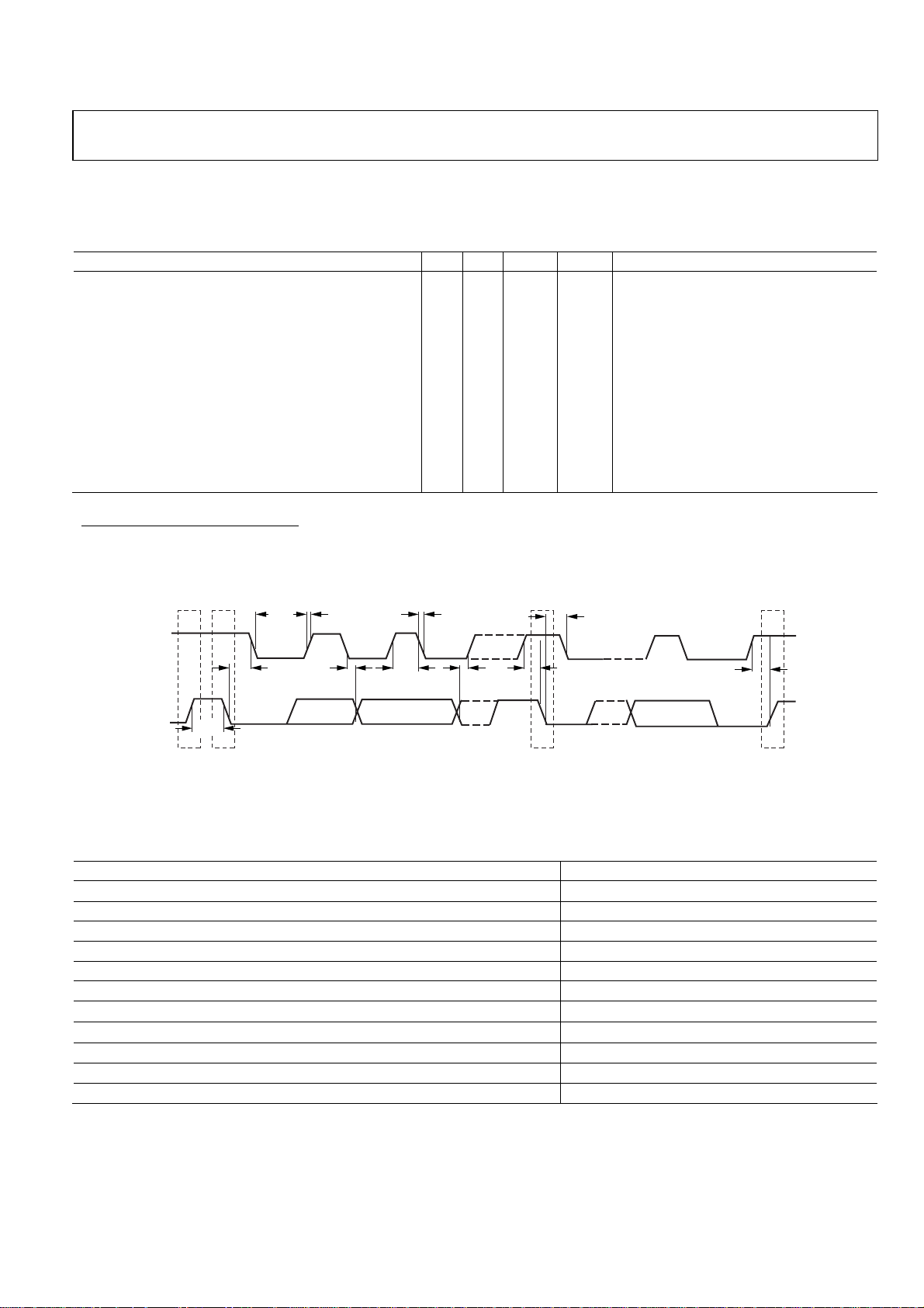
Table 2. (VDD = 2.7 V to 3.3 V, or 4.75V to 5.25V, GND = 0 V; Input Logic 0 = 0 V; Input Logic 1 = VDD; –40°C to +125°C, unless otherwise noted.)
Parameter Min Typ Max Unit Test Conditions/Comments
SERIAL INTERFACE
SCL Frequency 0 400 kHz
SCL High Pulse Width, t
SCL Low Pulse Width, t
SCL, SDA Rise Time, tR 0.3 µs
SCL, SDA Fall Time, t
Hold Time (Start Condition), t
Setup Time (Start Condition), t
Data Setup Time, t
Setup Time (Stop Condition), t
Data Hold Time, t
Bus Free Time (Between Stop and Start Condition, t
1
Sample tested during initial release to ensure compliance.
2
All input signals are specified with input rise/fall times = 3 ns, measured between the 10% and 90% points. Timing reference points at 50% for inputs and outputs.
Output load = 10 pF.
1, 2
See Figure 3
0.6 µs
HIGH
1.3 µs
LOW
F
0.6 µs After this period, the first clock is generated
HD;STA
0.6 µs Relevant for repeated start condition
SU;STA
0.1 µs
SU;DAT
0.6 µs
SU;STO
(Master) 0 µs
HD;DAT
t
R
t
LOW
0.3 µs
1.3 µs
BUF
t
F
t
HD:STA
SCL
SD
t
t
BUF
PS
HD:STA
t
HD:DAT
t
HIGH
t
SU:DAT
Figure 3.Serial Inter face Timing Diagram
t
SU:STA
S
t
SU:STO
P
04918-0-002
ABSOLUTE MAXIMUM RATINGS
Table 3. (TA = 25°C, unless otherwise noted.)
Parameter Rating
Positive Supply Voltage VDD to GND
Voltage on any input or output pin to GND –0.3 V to VDD + 0.3 V
ESD Rating (ESD Association Human Body Model, S5.1) TBD V
Operating Temperature Range –40°C to +125°C
Storage Temperature Range –65°C to +150°C
Junction Temperature 150°C
TSSOP Package θJA Thermal Impedance to Air
TSSOP Package θJC Thermal Impedance to Case
Lead Temperature, Soldering
Vapor Phase (60 sec) 215°C
Infrared (15 sec) 220°C
Stresses above those listed under Absolute Maximum Ratings may cause permanent damage to the device. This is a stress rating only;
functional operation of the device at these or any other conditions above those indicated in the operational section of this specification is
not implied. Exposure to absolute maximum rating conditions for extended periods may affect device reliability.
−0.3 V to +6.5 V
128 °C/W
14 °C/W
Rev. PrF | Page 5 of 17
Page 6

AD7745/AD7746
Preliminary Technical Data
OUTPUT NOISE AND RESOLUTION SPECIFICATIONS
The AD7745/46 resolution is limited by noise. The noise performance varies with the selected conversion time.
The Table 4 and Table 5 show typical noise performance and resolution for the capacitive channel. These numbers were generated from
1000 data samples acquired in continuous conversion mode, V
RMS noise represents standard deviation, p-p noise represents difference between minimum and maximum result in the data.
Effective resolution is calculated from RMS noise, p-p resolution is calculated from p-p noise.
Table 4. Typical Capacitive Input Noise and Resolution versus Conversion Time, CAP CHOP = 0
= 5.0V, all CIN and EXC pins open circuit.
DD
Conversion Time
(ms)
11.0 90.9 40.0 212.4 17.6 15.2
11.9 83.8 27.3 137.7 18.2 15.9
20.0 50.0 12.2 82.5 19.4 16.6
38.0 26.3 7.3 50.3 20.1 17.3
62.0 16.1 5.4 33.7 20.5 17.9
77.0 13.0 4.9 28.3 20.7 18.1
92.0 10.9 4.4 27.8 20.8 18.2
109.6 9.1 4.4 27.3 20.8 18.2
Output Data Rate
(Hz)
RMS Noise
(aF)
P-P Noise
(aF)
Effective Resolution
(Bits)
P-P Resolution
(Bits)
Table 5. Typical Capacitive Input Noise and Resolution versus Conversion Time, CAP CHOP = 1
Conversion Time
(ms)
20.1 49.8 31.7 159.2 18.0 15.7
22.0 45.6 24.9 118.2 18.3 16.1
38.1 26.3 9.8 63.0 19.7 17.0
74.1 13.5 4.9 31.7 20.7 18.0
122.1 8.2 3.9 26.4 21.0 18.2
152.1 6.6 3.4 21.5 21.2 18.5
182.1 5.5 2.9 18.6 21.4 18.8
217.3 4.6 2.9 18.6 21.4 18.8
Output Data Rate
(Hz)
RMS Noise
(aF)
P-P Noise
(aF)
Effective Resolution
(Bits)
P-P Resolution
(Bits)
Rev. PrF | Page 6 of 17
Page 7

Preliminary Technical Data
PIN CONFIGURATION AND FUNCTION DESCRIPTIONS
AD7745/AD7746
1
SCL
2
RDY
3
EXCA
4
5
6
-
)
7
-
)
8
AD7745
TOP VIEW
(Not toScale)
EXCB
REFIN(+)
REFIN(
CIN1(
CIN1(+)
Figure 4. AD7745 Pin Configuration (16-Lead TSSOP)
16
SDA
15
NC
14
VDD
13
GND
12
VIN(
-
)
11
VIN(+)
10
NC
9
NC
SCL
RDY
EXCA
EXCB
REFIN(+)
REFIN(
CIN1(
CIN1(+)
1
2
3
4
5
6
-
)
7
-
)
8
AD7746
TOP VIEW
(Not toScale)
Figure 5. AD7746 Pin Configuration (16-Lead TSSOP)
Table 6. Pin Function Descriptions
Pin No. Mnemonic Description
1 SCL Serial interface clock input. Connects to the master’s clock line.
(Requires pull-up resistor if not already provided in the system.)
2
RDY
Logic output. A falling edge on this output indicates that a conversion on enabled channel(s) has been finished and the new data are available. Alternatively, the status register
can be read via the 2-wire serial interface and the relevant bit(s) decoded to query finished conversion.
If not used, this pin should be left open circuit.
3, 4 EXCA, EXCB
CDC excitation outputs. The measured capacitance is connected between one of the EXC
pins and one of the CIN pins.
If not used, these pins should be left open circuit.
5, 6 REFIN(+), REFIN(–)
Differential voltage reference input for the voltage channel (ADC). Alternatively, the onchip internal reference can be used for the voltage channel. These reference input pins
are not used for conversion on capacitive channel(s) (CDC).
If not used, these pins can be left open circuit or connected to GND.
7 CIN1(-)
CDC negative capacitive input in differential mode. This pin is internally disconnected in
single ended CDC configuration.
If not used, this pin can be left open circuit or connected to GND.
8 CIN1(+)
CDC capacitive input (in single ended mode) or positive capacitive input (in differential
mode). The measured capacitance is connected between one of the EXC pins and one of
the CIN pins.
If not used, this pin can be left open circuit or connected to GND.
9 CIN2(+)
AD7746 only. CDC second capacitive input (in single ended mode) or positive capacitive
input (in differential mode).
If not used, this pin can be left open circuit or connected to GND.
10 CIN2(-)
AD7746 only. CDC negative capacitive input in differential mode. This pin is internally
disconnected in single ended CDC configuration.
If not used, this pin can be left open circuit or connected to GND.
11, 12 VIN(+), VIN(–)
Differential voltage input for the voltage channel (ADC). These pins are also used to connect an external temp sensing diode.
If not used, these pins can be left open circuit or connected to GND.
13 GND Ground pin.
14 VDD
Power supply voltage. This pin should be decoupled to GND, using a low impedance
capacitor, for example combination of 10uF tantalum and 0.1uF multilayer ceramic.
15 NC Not connected. This pin should be left open circuit.
16 SDA
Serial interface bidirectional data. Connects to the master’s data line. Requires pull-up
resistor if not provided elsewhere in the system.
16
15
14
13
12
11
10
9
SDA
NC
VDD
GND
-
VIN(
VIN(+)
CIN2(
CIN2(+)
)
-
)
Rev. PrF | Page 7 of 17
Page 8

AD7745/AD7746
SERIAL INTERFACE
The AD7745/AD7746 supports an I2C compatible two wire
serial interface. The two wires on the I2C Bus are called SCL,
(clock) and SDA, (data). These two wires carry all addressing,
control and data information one bit at a time over the bus to all
connected peripheral devices. The SDA wire carries the data,
while the SCL wire synchronizes the sender and receiver during
the data transfer. I2C devices are classified as either a MASTER
or SLAVE devices. A device that initiates a data transfer message
is called a master, while a device that responds to this message is
called a slave.
To control the AD7745/AD7746 device on the bus the following
protocol must be followed. First, the master initiates a data
transfer by establishing a START CONDITION, defined by a
high-to-low transition on SDA while SCL remains high. This
indicates that the START BYTE will follow next. This 8 bit, start
byte is made up of a 7 bit address plus an R/W bit indicator.
All peripherals connected to the bus respond to the start condition and shift in the next eight bits (7-bit address + R/W bit).
The bits arrive MSB first. The peripheral that recognizes the
transmitted address responds by pulling the data line low during the ninth clock pulse. This is known as the
ACKNOWLEDGE bit. All other devices withdraw from the bus
at this point and maintain an IDLE CONDITION. An exception
to this is the GENERAL CALL address which is described later
in this document. The idle condition is where the device monitors the SDA and SCL lines waiting for the start condition and
the correct address byte. The R/W bit determines the direction
of the data transfer. A logic ‘0’ LSB in the start byte means that
the master will write information to the addressed peripheral. In
this case the AD7745/AD7746 becomes a slave receiver. A logic
‘1’ LSB in the start byte means that the master will read information from the addressed peripheral. In this case the
AD7745/AD7746 becomes a slave transmitter. In all instances,
the AD7745/AD7746 acts as a standard slave device on the I2C
bus.
The start byte address for the AD7745/AD7746 is 0x90 for a
Write and 0x91 for a Read.
WRITE OPERATION
When a WRITE is selected, the byte following the start byte is
always the register ADDRESS POINTER (sub-address) byte,
which points to of one of the internal registers on the
AD7745/AD7746. The address pointer byte is automatically
loaded into the address pointer register and acknowledged by
the AD7745/AD7746. After the address pointer byte acknowledge, a STOP CONDITION, REPEATED START
CONDITION, or another data byte can follow from the master.
A stop condition is defined by a low-to-high transition on SDA
while SCL remains high. If a stop condition is ever encountered
by the AD7745/AD7746, it will return to its idle condition and
the address pointer is reset to address 0x00.
Preliminary Technical Data
If a data byte is transmitted after the register address pointer
byte, the AD7745/AD7746 will load this byte into the register
that is currently addressed by the address pointer register, send
an acknowledge and the address pointer auto-incrementer will
automatically increment the address pointer register to the next
internal register address. Thus subsequent transmitted data
bytes will be loaded into sequentially incremented addresses.
If a repeated start condition is encountered after the address
pointer byte, all peripherals connected to the bus respond exactly as outlined above for a start condition, i.e. a repeated start
condition is treated the same as a start condition. (When a master device issues a stop condition, it relinquishes control of the
bus, allowing another master device to take control of the bus.
Hence, a master wanting to retain control of the bus will issue
successive start conditions known as repeated start conditions).
READ OPERATION
When a READ is selected in the start byte, the register that is
currently addressed by the address pointer is transmitted on to
the SDA line by the AD7745/AD7746. This is then clocked out
by the master device and the AD7745/AD7746 will await an
acknowledge from the master.
If an acknowledge is received from the master, the address autoincrementer will automatically increment the address pointer
register and output the next addressed registers contents on to
the SDA line for transmission to the master. If no acknowledge
is received the AD7745/AD7746 returns to its idle state and the
address pointer is not incremented.
The address pointers’ auto-incrementer allows block data to be
written or read from the starting address and subsequent incremental addresses. The user can also access any unique
register (address) on a one-to-one basis without having to update all the registers. The address pointer register contents cannot be read.
If an incorrect address pointer location is accessed or, if the user
allows the auto incrementer to exceed the required register address, the following applies:
1. In Read Mode, the AD7745/AD7746 will continue to out-
put various internal register contents until the master
device issues a not-acknowledge, start or stop condition.
The address pointers’ auto-incrementer’s contents will reset
to point to the STATUS REGISTER at address 0x00 when a
stop condition is received at the end of a read operation.
This allows the status register to be read (polled) continually without having to constantly write to address pointer.
2. In Write Mode, the data for the invalid address will not be
loaded into the AD7745/AD7746 registers but an acknowledge will be issued by the AD7745/AD7746.
Rev. PrF | Page 8 of 17
Page 9

Preliminary Technical Data
GENERAL CALL
When a master issues a slave address consisting of seven zeros
with the eighth bit (R/W bit) set to zero, this is known as the
general call address. The general call address is for addressing
every device connected to the I2C bus. The AD7745/AD7746
will acknowledge this address and read in the following data
byte.
If the second byte is 0x06, the AD7745/AD7746 will reset completely uploading all default values. The AD7745/AD7746 will
not acknowledge any other general call commands.
SDATA
AD7745/AD7746
AD7745/AD7746 RESET
In order that the AD7745/AD7746 can be reset without having
to reset the entire I2C bus, an explicit reset command is provided. This uses a particular address pointer word as a
command word to reset the part and upload all default settings.
The reset command address word is 0xBF.
SCLOCK
1–7 8 9 1–7 8 9 1–7 8 9 PS
START ADDR
ACK SUBADDRESS ACK DATA ACK STOP
R/W
Figur e 6. Bus Data Tran sfer
02980-A-034
WRITE
SEQUENCE
READ
SEQUENCE
LSB = 0
S SLAVE ADDR A(S) SUB ADDR A(S) S SLAVE ADDR A(S) DATA
S = START BIT
P = STOP BIT
A(S) = ACKNOWLEDGE BY SLAVE
A(M) = ACKNOWLEDGE BY MASTER
Figure 7. Write and Read Sequences
DATA A(S)S SLAVE ADDR A(S) SUB ADDR A(S)
LSB = 1
A(S) = NO-ACKNOWLEDGE BY SLAVE
A(M) = NO-ACKNOWLEDGE BY MASTER
DATA P
A(M)
A(S)
DATA P
A(M)
02980-A-035
Rev. PrF | Page 9 of 17
Page 10

AD7745/AD7746
Preliminary Technical Data
REGISTER DESCRIPTIONS
The master can write to or read from all of the
AD7745/AD7746 registers except the address pointer register,
which is a write-only register. The address pointer register determines which register the next read or write operation
accesses. All communications with the part through the bus
start with an access to the address pointer register.
Table 7. Register Summary
Register
Status 0 0x00 R
Cap Data H 1 0x01 R Capacitive channel data – High byte 0x00
Cap Data M 2 0x02 R Capacitive channel data – Middle byte 0x00
Cap Data L 3 0x03 R Capacitive channel data – Low byte 0x00
VT Data H 4 0x04 R Voltage / Temperature channel data – High byte 0x00
Address
Pointer
(dec) (hex) (Default Value)
Dir Bit 7 Bit 6 Bit 5 Bit 4 Bit 3 Bit 2 Bit 1 Bit 0
- - - - EXCERR RDY RDYVT RDYCAP
0 0 0 0 0 1 1 1
After the part has been accessed over the bus and a read/write
operation is selected, the address pointer register is set up. The
address pointer register determines to/from which register the
operation takes place. A read/write operation is performed from
to the target address, which then increments to the next address
until a stop command on the bus is performed.
VT Data M 5 0x05 R Voltage / Temperature channel data – Middle byte 0x00
VT Data L 6 0x06 R Voltage / Temperature channel data – Low byte 0x00
Cap Setup 7 0x07 R/W
VT Setup 8 0x08 R/W
Exc Setup 9 0x09 R/W
Configuration 10 0x0A R/W
Cap DAC A 11 0x0B R/W
Cap DAC B 12 0x0C R/W
Cap Offset H 13 0x0D R/W Capacitive offset calibration – High byte 0x80
Cap Offset L 14 0x0E R/W Capacitive offset calibration – Low byte 0x00
Cap Gain H 15 0x0F R/W Capacitive gain calibration – High byte Factory calibrated
Cap Gain L 16 0x10 R/W Capacitive gain calibration – Low byte Factory calibrated
CAPEN CIN21 CAPDIFF - - - CAPCHOP
0 0 0 0 0 0 0 0
VTEN VTMD1 VTMD0 EXTREF - - VTSHORT VTCHOP
0 0 0 0 0 0 0 0
CLKCTRL EXCON EXCB
0 0 0 0 0 0 1 1
VTFS1 VTFS0 CAPFS2 CAPFS1 CAPFS0 MD2 MD1 MD0
1 0 1 0 0 0 0 0
DACAENA DACA – 7-Bit Value
0 0x00
DACBENB DACB – 7-Bit Value
0 0x00
EXCB
EXCA
EXCA
EXCLVL1 EXCLVL0
Volt Gain H 17 0x11 R/W Voltage gain calibration – High byte Factory calibrated
Volt Gain L 18 0x12 R/W Voltage gain calibration – Low byte Factory calibrated
1
The CIN2 bit is relevant only for AD7746. The CIN2 bit should be always 0 on AD7745.
Rev. PrF | Page 10 of 17
Page 11

Preliminary Technical Data
STATUS REGISTER
Address pointer 0x00, read only, default value 0x07
Indicates status of the converter. Status register can be read via
the 2-wire serial interface to query a finished conversion.
Bit Bit 7 Bit 6 Bit 5 Bit 4 Bit 3 Bit 2 Bit 1 Bit 0
Mnemonic - - - - EXCERR RDY RDYVT RDYCAP
Default 0 0 0 0 0 1 1 1
Bit Mnemonic Description
7-4 - Not used, always read 0
3 EXCERR
2 RDY
1 RDYVT
0 RDYCAP
CAP DATA REGISTER
24 bits, address pointer 0x01, 0x02, 0x03, read only,
default value 0x000000
Capacitive channel output data. The register is updated after
finished conversion on the capacitive channel, with one exception: When the serial interface read operation from the CAP
DATA register is in progress, the data register is not updated
and the new capacitance conversion result is lost.
Stop condition on the serial interface is considered as the end of
the read operation. Therefore, to prevent data corruption, all 3
bytes of the data register should be read subsequently using the
register address pointer auto-increment feature of the serial
interface.
To prevent losing some of the results, the CAP DATA register
should be read before the next conversion on the capacitive
channel is finished.
Code 0x000000 represents negative full-scale (-4.096 pF),
code 0x800000 represents zero scale (0 pF) and the code
0xFFFFFF represents positive full scale (+4.096 pF).
EXCERR = 1 indicates that the excitation output cannot be driven properly.
The possible reason can be short or too high capacitance between the excitation pin and ground.
RDY = 0 indicates that conversion on the enabled channel(s) has been finished and new unread data are available.
If both capacitive and voltage / temperature channels are enabled, thy RDY bit will be changed to 0 after conversion on both channels is finished. The RDY bit will return to 1 either when data are read or prior finishing
the next conversion.
If only one channel is enabled, for example capacitive, then the RDY bit will reflect the RDYCAP bit.
RDYVT = 0 indicates that a conversion on the voltage / temperature channel has been finished and new unread data are available.
RDYCAP = 0 indicates that a conversion on the capacitive channel has been finished and new unread data are
available.
RDY
The
pin high to low transition can be used as an alternative indication of the finished conversion.
VT DATA REGISTER
24 bits, address pointer 0x04, 0x05, 0x06, read only,
default value 0x000000
Voltage / Temperature channel output data. The register is updated after finished conversion on the voltage channel or
temperature channel, with one exception: When the serial interface read operation from the VT DATA register is in progress,
the data register is not updated and the new voltage / temperature conversion result is lost.
Stop condition on the serial interface is considered as the end of
the read operation. Therefore, to prevent data corruption, all 3
bytes of the data register should be read subsequently using the
register address pointer auto-increment feature of the serial
interface.
For voltage input, code 0 represents negative full scale (-V
code 0x800000 represents zero scale (0 V) and the code
0xFFFFFF represents positive full scale (+V
To prevent losing some of the results, the VT DATA register
should be read before the next conversion on the voltage /temperature channel is finished.
For temperature sensor, the temperature can be calculated from
code using equation:
Temperature (°C) = (Code / 2048) - 4096
pin reflects status of the RDY bit. Therefore, the
AD7745/AD7746
RDY
),
REF
).
REF
Rev. PrF | Page 11 of 17
Page 12

AD7745/AD7746
Preliminary Technical Data
CAP SETUP REGISTER
Address pointer 0x07, default value 0x00
Capacitive channel setup.
Bit Bit 7 Bit 6 Bit 5 Bit 4 Bit 3 Bit 2 Bit 1 Bit 0
Mnemonic CAPEN CIN2 DIFF - - - - CAPCHOP
Default 0 0 0 0 0 0 0 0
Bit Mnemonic Description
7 CAPEN CAPEN = 1 enables capacitive channel for single conversion, continuous conversion or calibration.
6 CIN2 CIN2 = 1 switches the internal multiplexer to the second capacitive input on the AD7746.
5 DIFF DIFF = 1 sets differential mode on the selected capacitive input.
4-1 - These bits must be 0 for proper operation.
0 CAPCHOP CAPCHOP = 1 enables chopping on the capacitive channel.
VT SETUP REGISTER
Address pointer 0x08, default value 0x00
Voltage / Temperature channel setup.
Bit Bit 7 Bit 6 Bit 5 Bit 4 Bit 3 Bit 2 Bit 1 Bit 0
Mnemonic VTEN VTMD1 VTMD0 EXTREF - - VTSHORT VTCHOP
Default 0 0 0 0 0 0 0 0
Bit Mnemonic Description
7 VTEN VTEN = 1 enables voltage / temperature channel for single conversion, continuous conversion or calibration.
Voltage / temperature channel input configuration:
VTMD1 VTMD0 Channel Input
6
5
VTMD1
VTMD0
0 0 Internal Temperature Sensor
0 1 External Temperature Sensor Diode
1 0 VDD Monitor
1 1 External Voltage Input (VIN)
EXTREF = 1 selects an external reference voltage connected to REFIN(+), REFIN(–) for the voltage input or the
V
Monitor.
4 EXTREF
3-2 - These bits must be 0 for proper operation.
1 VTSHORT VTSHORT = 1 internally shorts the voltage / temperature channel input for test purposes.
0
VTCHOP = 1
DD
EXTREF = 0 selects the on-chip internal reference. The internal reference must be used with the internal temperature sensor for proper operation.
VTCHOP = 1 sets internal chopping on the voltage / temperature channel.
The VTCHOP bit must be set to 1 for the specified voltage / temperature channel performance.
Rev. PrF | Page 12 of 17
Page 13

Preliminary Technical Data
AD7745/AD7746
EXC SETUP REGISTER
Address pointer 0x09, default value 0x03
Capacitive channel excitation setup.
Bit Bit 7 Bit 6 Bit 5 Bit 4 Bit 3 Bit 2 Bit 1 Bit 0
Mnemonic CLKCTRL EXCON EXCB
EXCB
EXCA
EXCA
Default 0 0 0 0 0 0 0 0
Bit Mnemonic Description
7 CLKCTRL
CLKCTRL = 1 decreases the excitation signal frequency and the modulator clock frequency by factor of 2.
This also increases the conversion time on all channels (capacitive, voltage and temperature) by factor of 2.
When EXCON = 0, the excitation signal is present on the output only during capacitance channel conversion
6 EXCON
When EXCON = 1, the excitation signal is present on the output during both capacitance and voltage / temperature conversion
5 EXCB EXCB = 1 enables EXCB pin as the excitation output
EXCB
4
EXCB
= 1 enables EXCB pin as the inverted excitation output
Only one of the EXCB or the
EXCB
bits should be set for proper operation.
3 EXCA EXCA = 1 enables EXCA pin as the excitation output
EXCA
2
EXCA
= 1 enables EXCA pin as the inverted excitation output
Only one of the EXCA or the
EXCA
bits should be set for proper operation.
Excitation Voltage Level:
EXCLVL1 EXCLVL0 Voltage on Cap. EXC pin Low Level EXC pin High Level
1
0
EXCLVL1,
EXCLVL0
0 0 ±VDD/8 V
0 1 ±VDD/4 V
1 0 ±V
1 1 ±VDD/2 0 VDD
× 3/8 V
DD
× 3/8 V
DD
× 1/4 V
DD
× 1/8 V
DD
EXCLVL1 EXCLVL0
× 5/8
DD
× 3/4
DD
× 7/8
DD
Rev. PrF | Page 13 of 17
Page 14

AD7745/AD7746
Preliminary Technical Data
CONFIGURATION REGISTER
Address pointer 0x0A, default value 0xA0
Converter update rate and mode of operation setup.
Bit Bit 7 Bit 6 Bit 5 Bit 4 Bit 3 Bit 2 Bit 1 Bit 0
Mnemonic VTF1 VTF0 CAPF2 CAPF1 CAPF0 MD2 MD1 MD0
Default 0 0 0 0 0 0 0 0
Bit Mnemonic Description
Voltage / temperature channel digital filter setup - conversion time / update rate setup.
The conversion times in this table are valid for the CLKCTRL = 0 in the EXC SETUP register. The conversion
times are longer by factor of two for the CLKCTRL = 1.
7
6
5
4
3
2
1
0
VTF1
VTF0
CAPF2
CAPF1
CAPF0
MD2
MD1
MD0
VTCHOP = 1
VTF1 VTF0 Conversion
Time (ms)
0 0 20.1 49.8
0 1 32.1 31.2
1 0 62.1 16.1
1 1 122.1 8.2
Capacitive channel digital filter setup - conversion time / update rate setup.
The conversion times in this table are valid for the CLKCTRL = 0 in the EXC SETUP register. The conversion
times are longer by factor of two for the CLKCTRL = 1.
CAP CHOP = 1 CAP CHOP = 0
CAPF2 CAPF1 CAPF0 Conversion
Time (ms)
0 0 0 20.1 49.8 11.0 90.9
0 0 1 22.0 45.6 11.9 83.8
0 1 0 38.1 26.3 20.0 50.0
0 1 1 74.1 13.5 38.0 26.3
1 0 0 122.1 8.2 62.0 16.1
1 0 1 152.1 6.6 77.0 13.0
1 1 0 182.1 5.5 92.0 10.9
1 1 1 217.3 4.6 109.6 9.1
Converter mode of operation setup
MD2 MD1 MD0 Mode
0 0 0 Idle
0 0 1 Continuous Conversion
0 1 0 Single Conversion
0 1 1 Power-Down
1 0 0 1 0 1 Capacitance Offset Calibration
1 1 0 Capacitance or Voltage Gain Calibration
1 1 1
Update Rate
(Hz)
Update Rate
(Hz)
Conversion
Time (ms)
Update Rate
(Hz)
Rev. PrF | Page 14 of 17
Page 15

Preliminary Technical Data
AD7745/AD7746
CAP DAC A REGISTER
Address pointer 0x0B, default value 0x00
Capacitive DAC setup.
Bit Bit 7 Bit 6 Bit 5 Bit 4 Bit 3 Bit 2 Bit 1 Bit 0
Mnemonic DACAENA DACA – 7-Bit Value
Default 0 0x00
Bit Mnemonic Description
7 DACAENA DACAENA = 1 connects capacitive DAC A to the positive capacitance input.
6-1 DACA
DAC A value, code 0x00 ≈ 0pF, code 0x7F ≈ Full Range
CAP DAC B REGISTER
Address pointer 0x0C, default value 0x00
Capacitive DAC setup.
Bit Bit 7 Bit 6 Bit 5 Bit 4 Bit 3 Bit 2 Bit 1 Bit 0
Mnemonic DACBENB DACB – 7-Bit Value
Default 0 0x00
Bit Mnemonic Description
7 DACBENB DACBENB = 1 connects capacitive DAC B to the positive capacitance input.
6-1 DACB
DAC B value, code 0x00 ≈ 0pF, code 0x7F ≈ Full Range
CAP OFFSET REGISTER
16 bits, address pointer 0x0D, 0x0E default value 0x8000
Capacitive offset calibration register. The register holds capacitive channel zero-scale calibration coefficient. The value in this register is
used to digitally remove the capacitive channel offset. The value in this register is updated automatically following the execution of a capacitance offset calibration. The capacitive offset calibration resolution (cap offset register LSB) is less than 32 aF, the full range is 1 pF. On
the AD7746, the register is shared by the two capacitive channels.
CAP GAIN REGISTER
16 bits, address pointer 0x0F, 0x10, default value 0xXXXX
Capacitive gain calibration register. The register holds capacitive channel full scale factory calibration coefficient.
VOLT GAIN REGISTER
16 bits, address pointer 0x11,0x12, default value 0xXXXX
Voltage gain calibration register. The register holds voltage channel full scale factory calibration coefficient.
Rev. PrF | Page 15 of 17
Page 16

AD7745/AD7746
TYPICAL APPLICATION DIAGRAM
TEMP
VIN(+)
VIN(
C
IN1
C
IN1
EXC1
EXC2
SENSOR
-
)
(+)
-
)
(
CAP DAC
CAP DAC
EXCITATION
MUX
CLOCK
GENERATOR
24-BITΣ-
MODULATOR
∆
V
DD
DIGITAL
FILTER
CONTROL LOGIC
CALIBRATION
VOLTAGE
REFERENCE
0.1uF 10uF
AD7745
SERIAL
INTERFACE
Preliminary Technical Data
+3V / +5V
+
POWER SUPPLY
HOST
SYSTEM
I2C
SDA
SCL
RDY
RTD
REFIN(+) REFIN(-)
GND
Figure 8. Basic Application Diagram for a Differential Capacitive Sensor
+
V
DD
REFIN(+)
CLOCK
GENERATOR
24-BITΣ-
MODULATOR
REFIN(-)
R
REF
∆
DIGITAL
FILTER
VOLTAGE
REFERENCE
VIN(+)
VIN(
C
IN1
C
IN1
CAPACITIVE
SENSOR
EXC1
EXC2
TEMP
SENSOR
-
)
(+)
-
)
(
CAP DAC
CAP DAC
EXCITATION
MUX
Figure 9. Application Diagram for a Single Capacitive Sensor and an External RTD or PTC Sensor
0.1uF 10uF
AD7745
SERIAL
INTERFACE
CONTROL LOGIC
CALIBRATION
GND
I2C
+3V / +5V
POWER SUPPLY
SYSTEM
SDA
SCL
RDY
RDY
HOST
Rev. PrF | Page 16 of 17
Page 17

Preliminary Technical Data
PR05468-0-3/05(PrF)
OUTLINE DIMENSIONS
5.10
5.00
4.90
AD7745/AD7746
16
4.50
4.40
4.30
PIN 1
0.15
0.05
0.65
BSC
COPLANARITY
COMPLIANT TO JEDEC STANDARDS MO-153AB
Figure 10. 16-Lead Thin Shrink Small Outline Package [TSSOP] (RU-16)
9
6.40
BSC
81
1.20
MAX
0.20
SEATING
PLANE
0.09
0.30
0.19
0.10
Dimensions shown in millimeters
8°
0°
0.75
0.60
0.45
ESD CAUTION
ESD (electrostatic discharge) sensitive device. Electrostatic charges as high as 4000 V readily accumulate on the
human body and test equipment and can discharge without detection. Although this product features proprietary ESD protection circuitry, permanent damage may occur on devices subjected to high energy electrostatic
discharges. Therefore, proper ESD precautions are recommended to avoid performance degradation or loss of
functionality.
2
Purchase of licensed I
chaser under the Philips I
Standard Specification as defined by Philips.
C components of Analog Devices or one of its sublicensed Associated Companies conveys a license for the pur-
2
C Patent Rights to use these components in an I2C system, provided that the system conforms to the I2C
© 2005 Analog Devices, Inc. All rights reserved. Trademarks and registered trademarks are the property of th eir respective companies.
 Loading...