

Page 1
16-Bit 900 kSPS - ADC with a
2.5V
REFERENCE
POST-
PROCESSOR
DEFAULT FILTER
(ROM )
XTAL
CLOCK
PRESET
FILTER
MOD
CONTROL
LOGIC
UNI
HALF
PWR
STBY
SYNC
S/P
V
IN
(+)
V
IN
(–)
RD/ WR
SOE/ CS
CFMT/RS
DVAL/ INT
SDI/DB0
ERR/ DB1
DB2
DB3
RESETCFG/DB4
INT/DB5
FSI/ DB6
SCO/ DB7
SDO/ DB8
SCR/ DB13
CFGEND/DB12
DB11
DB10
FSO/DB9
SMODE1/ DB15
SMODE0/ DB14
XTAL_OFF
XTAL
CLKIN
DV
DD
DGND
REF2
REF1
AV
DD
AGND
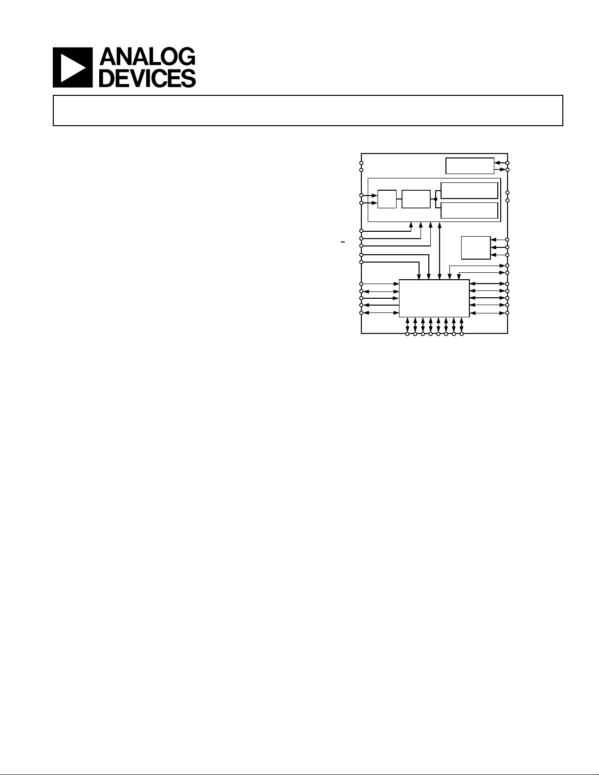
AD7725
Programmable Postprocessor
AD7725
FEATURES
Programmable Filtering:
Any Characteristic up to 108 Tap FIR and/or IIR
Polynomial Signal Conditioning up to 8
th
Order
Programmable Decimation and Output Word Rate
Flexible Programming Modes:
Boot from DSP or External EPROM
Parallel/Serial Interface
Internal Default Filter for Evaluation
14.4 MHz Max Master Clock Frequency
0 V to +4 V (Single-Ended) or 2 V (Differential) Input
Range
Power Supplies: AVDD, DVDD: 5 V 5%
On-Chip 2.5 V Voltage Reference
44-Lead MQFP Package
TYPICAL APPLICATIONS
Radar
Sonar
Auxiliary Car Functions
Medical Communications
GENERAL DESCRIPTION
The AD7725 is a complete 16-bit, - analog-to-digital converter with on-chip, user-programmable signal conditioning. The
output of the modulator is processed by three cascaded finite
impulse response (FIR) filters, followed by a fully user-programmable postprocessor. The postprocessor provides processing
power of up to 130 million accumulates (MAC) per second. The
user has complete control over the filter response, the filter coefficients, and the decimation ratio.
The postprocessor permits the signal conditioning characteristics
to be programmed through a parallel or serial interface.
is programmed by loading a user-defined filter in the form of a
configuration file. This filter can be loaded from a DSP or an
external serial EPROM. It is generated using a digital filter
design package called Filter Wizard, which is available from the
AD7725 section on the Analog
Devices
website.
FUNCTIONAL BLOCK DIAGRAM
t
Filter Wizard allows the user
and generates the appropriate
loaded to the postprocessor. The
o design different filter types
configuration file to be down-
AD7725 also has an internal
default filter for evaluation purposes.
It provides 16-bit performance for input bandwidths up to
350 kHz with an output word rate of 900 kHz maximum. The
input sample rate is set either by the crystal oscillator or an
external clock.
This part has an accurate on-chip 2.5 V reference for the modu-
It
lator. A reference input/output function allows either the
internal reference or an external system reference to be used as
the reference source for the modulator.
The device is available in a 44-lead MQFP package and is specified over a –40°C to +85°C temperature range.
REV. A
Information furnished by Analog Devices is believed to be accurate and
reliable. However, no responsibility is assumed by Analog Devices for its
use, nor for any infringements of patents or other rights of third parties that
may result from its use. No license is granted by implication or otherwise
under any patent or patent rights of Analog Devices. Trademarks and
registered trademarks are the property of their respective owners.
One Technology Way, P.O. Box 9106, Norwood, MA 02062-9106, U.S.A.
Tel: 781/329-4700 www.analog.com
Fax: 781/326-8703 © 2004 Analog Devices, Inc. All rights reserved.
Page 2

(AVDD = 5 V 5%, AGND = AGND1 = AGND2 = DGND = 0 V,
1
AD7725–SPECIFICATIONS
2
f
= 9.6 MHz, REF2 = 2.5 V, TA = T
CLKIN
MIN
to T
, unless otherwise noted.)
MAX
B Version
Parameter Test Conditions/Comments Min Typ Max Unit
DYNAMIC SPECIFICATIONS When tested with the FIR filter in
Figure 1, HALF_PWR = Logic High
Bipolar Mode
Signal-to-Noise
3
Measurement Bandwidth = 0.5 f
4
O
2.5 V Reference 77 83 dB
3 V Reference 79 85 dB
3, 5
Measurement Bandwidth = 0.5 f
4
O
–94 –86 dB
–98 –89 dB
83 dB
–94 dB
Total Harmonic Distortion
Spurious Free Dynamic Range
Unipolar Mode
Signal-to-Noise
3
Total Harmonic Distortion
3, 5
3, 5
ANALOG INPUTS
Full-Scale Input Span V
Bipolar Mode Differential or Single-Ended Input ±4/5 V
Unipolar Mode Single-Ended Input 0 8/5 V
Absolute Input Voltage V
Input Sampling Capacitance 2 pF
Input Sampling Rate, f
CLKIN
(+) – VIN(–)
IN
(+) and/or VIN(–) AGND AV
IN
14.4
DD
V
REF2
REF2
V
V
6
MHz
CLOCK
CLKIN Duty Ratio 45 55 %
REFERENCE
REF1 Output Resistance 3.5 kΩ
Reference Buffer
Offset Voltage Offset between REF1 and REF2 ±3mV
Using Internal Reference
REF2 Output Voltage 2.39 2.54 2.69 V
REF2 Output Voltage Drift 60 ppm/°C
Using External Reference
REF2 Input Impedance REF1 = AGND 8 kΩ
REF2 External Voltage Input
7
2.5 V
STATIC PERFORMANCE
Resolution 16 Bits
Differential Nonlinearity (DNL)
Integral Nonlinearity (INL)
3
3
Guaranteed Monotonic ±0.5 ±1
±2 LSB
8
LSB
DC CMRR 80 dB
Offset Error ±20 mV
Gain Error
3, 9
±0.5 %FSR
LOGIC INPUTS (Excluding CLKIN)
V
, Input High Voltage 2.0 V
INH
V
, Input Low Voltage 0.8 V
INL
CLOCK INPUT (CLKIN)
V
, Input High Voltage 0.7 DV
INH
V
, Input Low Voltage 0.3 DV
INL
DD
DD
V
V
REV. A–2–
Page 3
AD7725
B Version
Parameter Test Conditions/Comments Min Typ Max Unit
ALL LOGIC INPUTS
IIN, Input Current VIN = 0 V to DV
DD
CIN, Input Capacitance 10 pF
LOGIC OUTPUTS
, Output High Voltage |I
V
OH
VOL, Output Low Voltage |I
POWER SUPPLIES
AV
DD
11
AI
DD
DV
DD
13
DI
DD
Power Consumption
NOTES
1
Operating temperature range is as follows: B Version: –40°C to +85°C.
2
f
is the CLKIN frequency.
CLKIN
3
See Terminology section.
4
FO = output data rate.
5
When using the internal reference, THD and SFDR specifications apply only to input signals above 10 kHz with a 10 µF decoupling capacitor between REF2 and
AGND2. At frequencies below 10 kHz, THD degrades to –80 dB and SFDR degrades to –83 dB.
6
See Figures 23 and 24 for information regarding the number of filter taps allowed and the current consumption as the CLKIN frequency is varied.
7
The AD7725 can operate with an external reference input in the range of 1.2 V to 3.15 V.
8
Guaranteed by the design.
9
Gain Error excludes reference error.
10
All IDD tests are done with the digital inputs equal to 0 V or DVDD.
11
Analog current does not vary as the CLKIN frequency and the number of filter taps used in the postprocessor is varied.
12
If HALF_PWR is logic low, AIDD will typically double.
13
Digital current varies as the CLKIN frequency and the number of filter taps used in the postprocessor is varied. See Figures 23 and 24.
14
Digital inputs static and equal to 0 V or DVDD.
Specifications subject to change without notice.
10
14
| = 200 µA 4.0 V
OUT
| = 1.6 mA 0.4 V
OUT
HALF_PWR = Logic High
12
4.75 5.25 V
28 33 mA
4.75 5.25 V
With the Filter in Figure 1 84 90 mA
Standby Mode 30 mW
±10 µA
0
–20
–40
–60
–80
ATTENUATION – dB
–100
–120
–140
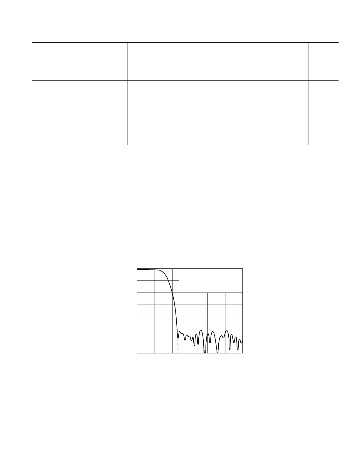
0 30050
CUTOFF FREQUENCY = 50kHz
STOP-BAND FREQUENCY = 116kHz
NUMBER OF FILTER TAPS USED IN
THE POSTPROCESSOR = 108
OUPUT DATA RATE = CLKIN/16
100 150 200 250
116
FREQUENCY – kHz
Figure 1. Digital Filter Characteristics Used for Specifications
REV. A
–3–
Page 4

AD7725
Preset Filter, Default Filter, and Postprocessor Characteristics
1, 2
Parameter Test Conditions/Comments Min Typ Max Unit
DIGITAL FILTER RESPONSE
PRESET FIR
Data Output Rate f
/8 Hz
CLKIN
Stop-Band Attenuation 70 dB
Low-Pass Corner Frequency f
Group Delay
Settling Time
3
3
/16 Hz
CLKIN
133/(2 f
133/f
CLKIN
)s
CLKIN
s
DEFAULT FILTER Internal FIR Filter Stored in ROM
Number of Taps 106
Frequency Response
0 kHz to f
/195.04 –3 dB
f
CLKIN
f
/184.08 –6 dB
CLKIN
/133.2 to f
f
CLKIN
Group Delay
Settling Time
Output Data Rate, f
/546.08 ± 0.001 dB
CLKIN
/2 –120 dB
CLKIN
3
3
O
2141/(2 f
2141/f
CLKIN
f
/32 Hz
CLKIN
)s
CLKIN
s
POSTPROCESSOR CHARACTERISTICS
Input Data Rate f
Coefficient Precision
4
24 Bits
/8 Hz
CLKIN
Arithmetic Precision 30 Bits
Number of Taps Permitted 108
Decimation Factor 2 256
Number of Decimation Stages 1 5
Output Data Rate f
NOTES
1
These characteristics are fixed by the design.
2
f
is the CLKIN frequency.
CLKIN
3
See Terminology section.
4
See the Configuration File Format section for more information.
/4096 f
CLKIN
/16 Hz
CLKIN
REV. A–4–
Page 5

TIMING SPECIFICATIONS
(AVDD = 5 V 5%; DVDD = 5 V 5%; AGND = DGND = 0 V, REF2 = 2.5 V,
unless otherwise noted.)
AD7725
1, 2
Parameter Symbol Min Typ Max Unit
CLKIN Frequency f
CLKIN Period (t
CLK
= 1/f
)t
CLKIN
CLKIN Low Pulse Width t
CLKIN High Pulse Width t
CLKIN Rise Time t
CLKIN Fall Time t
CLKIN to SCO Delay t
SCO Period: SCR = 0 t
SCR = 1 t
CLKIN
1
2
3
4
5
6
7
7
114.4MHz
0.07 1 µs
0.45 t
0.45 t
1
1
0.55 t
0.55 t
1
1
5ns
5ns
35 50 ns
1t
2t
SERIAL INTERFACE (DSP MODE ONLY)
FSI Setup Time before SCO Transition t
FSI Hold Time after SCO Transition t
SDI Setup Time t
SDI Hold Time t
8
9
10
11
30 ns
0ns
30 ns
0ns
SERIAL INTERFACE (DSP AND BFR MODES)
SCO Transition to FSO High Delay t
SCO Transition to FSO Low Delay t
SDO Setup before SCO Transition t
SDO Hold after SCO Transition t
12
13
14
15
0ns
20 ns
20 ns
10 ns
SERIAL INTERFACE (EPROM MODE)
SCO High Time t
SCO Low Time t
SOE Low to First SCO Rising Edge t
Data Setup before SCO Rising Edge t
16
17
18
19
22 ns
8t
8t
20 t
PARALLEL INTERFACE
DATA WRITE
RS Low to CS Low t
WR Setup before CS Low t
RS Hold after CS Rising Edge t
CS Pulse Width t
WR Hold after CS Rising Edge t
Data Setup Time t
Data Hold Time t
20
21
22
23
24
25
26
15 ns
15 ns
0ns
50 ns
0ns
10 ns
5ns
DATA READ
RS Low to CS Low t
RD Setup before CS Low t
RS Hold after CS Rising Edge t
RD Hold after CS Rising Edge t
Data Valid after CS Falling Edge
3
Data Hold after CS Rising Edge t
27
28
29
30
t
31
32
15 ns
15 ns
0ns
0ns
30 ns
10 ns
STATUS READ/INSTRUCTION WRITE
CS Duty Cycle t
Interrupt Clear after CS Low t
RD Setup to CS Low t
RD Hold after CS Rising Edge t
Read Data Access Time
3
Read Data Hold after CS Rising Edge t
Write Data Setup before CS Rising Edge t
Write Data Hold after CS Rising Edge t
NOTES
1
Guaranteed by design.
2
Guaranteed by characterization. All input signals are specified with tr tf 5 ns (10% to 90% of DVDD) and timed from a voltage level of 1.6 V.
3
Measured with the load circuit in Figure 2 and defined as the time required for the output to cross 0.8 V and 2.4 V.
33
34
35
36
t
37
38
39
40
1t
15 ns
15 ns
0ns
30 ns
10 ns
10 ns
5ns
CLK
CLK
CLK
CLK
CLK
CLK
REV. A
–5–
Page 6
AD7725
I
OL
1.6mA
TO
OUTPUT
PIN
25pF
C
L
I
OH
200A
1.6V
Figure 2. Load Circuit for Digital Output Timing Specifications
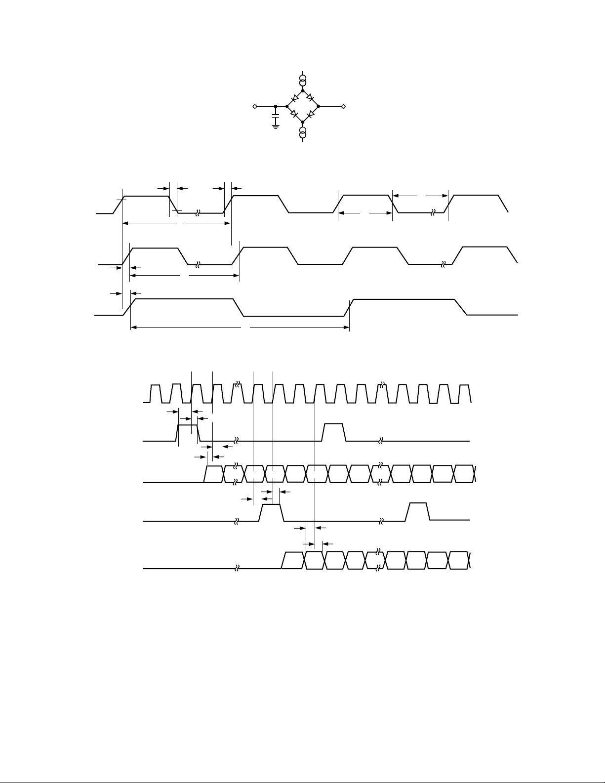
CLKIN
SCO
SCR = 0
SCO
SCR = 1
2.3V
CFMT = 0
SCO
FSI
SDI
t
5
0.8V
t
1
t
6
t
6
t
7
t
4
t
3
t
7
t
2
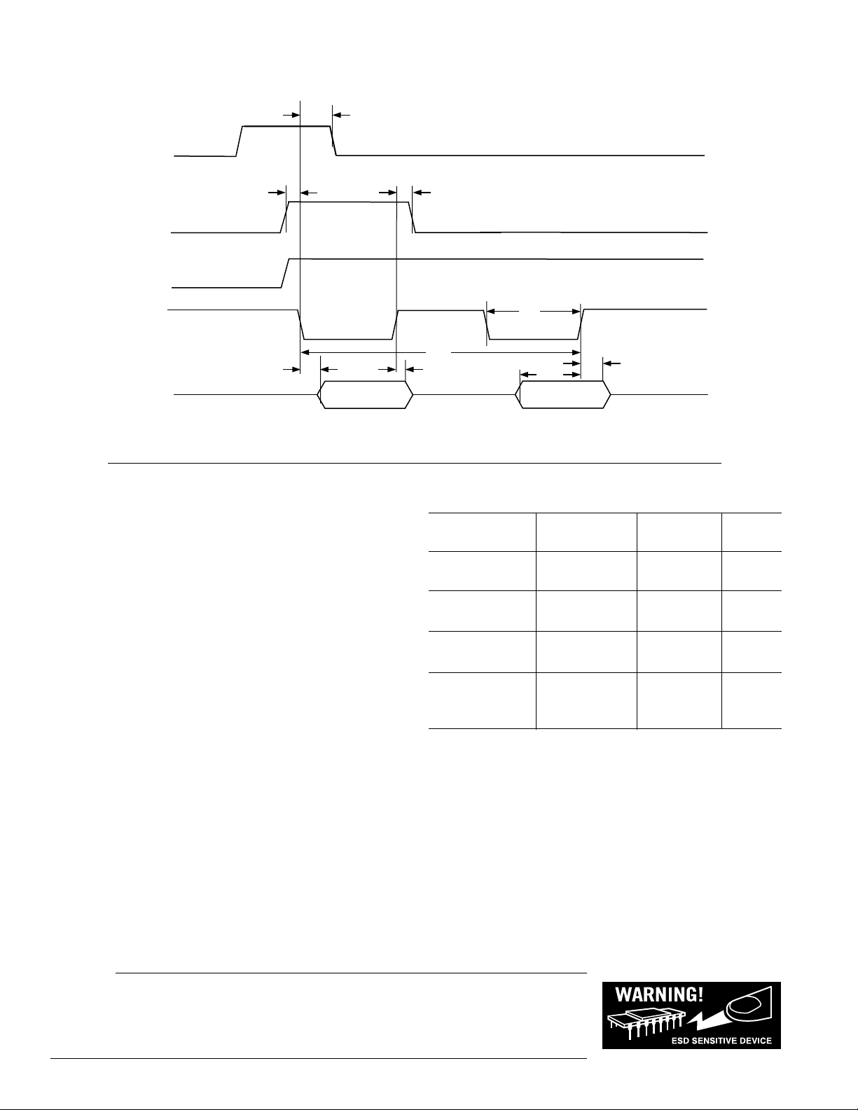
Figure 3. CLKIN to SCO Relationship
t
8
t
9
t
t
10
11
D15 D0 D15 D4 D3 D2 D1
D4 D2D3 D1
t
13
t
14
t
15
D15 D14 D13 D12 D1 D0 D15 D14
FSO
SDO
t
12
Figure 4. Serial Mode (DSP Mode and Boot from ROM (BFR) Mode). In BFR Mode, FSI and SDI are not used.
REV. A–6–
Page 7
S
INT
RD/WR
RS
CS
t
16
SCO
t
17
t
19
CO
SDI
t
18
Figure 5. Serial Mode (EPROM Mode)
t
21
t
20
AD7725
t
24
t
22
DB0 DB15
–
RD/WR
DB0 DB15
–
INT
RS
CS
t
23
THREE-STATE
t
t
26
25
VALID DATA
Figure 6. Parallel Mode (Writing Data to the AD7725)
t
THREE-STATE
28
t
27
t
t
31
23
VA LID DATA
t
30
t
29
t
32
Figure 7. Parallel Mode (Reading Data from the AD7725)
THREE-STATE
THREE-STATE
REV. A
–7–
Page 8
AD7725
INT
t
34
RD/WR
RS
CS
DB0 DB15
–
t
35
t
37
STATU
THREE-STATE THREE-STATE THREE-STATE
S
t
36
t
23
t
33
t
38
t
39
INSTRUCTI
ON
Figure 8. Parallel Mode (Reading the Status Register and Writing Instructions)
ABSOLUTE MAXIMUM RATINGS
(TA = 25°C, unless otherwise noted.)
to DGND . . . . . . . . . . . . . . . . . . . . . . . . –0.3 V to +7 V
DV
DD
to AGND . . . . . . . . . . . . . . . . . . . . . . . . . –0.3 V to +7 V
AV
DD
AV
DD
, AV
to DVDD . . . . . . . . . . . . . . . . . . . . –1 V to +1 V
DD1
1
ORDERING GUIDE
Temperature Package Package
Model Range Description Option
AD7725BS –40°C to +85°CMetric Quad S-44-2
AGND, AGND1 to DGND . . . . . . . . . . . . . –0.3 V to +0.3 V
Digital Inputs to DGND . . . . . . . . . . –0.3 V to DV
Digital Outputs to DGND . . . . . . . . . –0.3 V to DV
V
(+), VIN(–) to AGND . . . . . . . . . . . –0.3 V to AVDD + 0.3 V
IN
REF1 to AGND . . . . . . . . . . . . . . . . . –0.3 V to AV
REF2 to AGND . . . . . . . . . . . . . . . . . –0.3 V to AV
REFIN to AGND . . . . . . . . . . . . . . . . –0.3 V to AV
DGND, AGND . . . . . . . . . . . . . . . . . . . . . . . . . . . . . . . ± 0.3 V
Input Current to Any Pin except Supplies
I
(AI
DD
+ DIDD) . . . . . . . . . . . . . . . . . . . . . . . . . . . . 150 mA
DD
2
. . . . . . . . . ± 10 mA
Operating Temperature Range . . . . . . . . . . . .–40°C to +85°C
Storage Temperature Range . . . . . . . . . . . . . –65°C to +150°C
Junction Temperature . . . . . . . . . . . . . . . . . . . . . . . . . . 150°C
Thermal Impedance . . . . . . . . . . . . . . . . . . . . . . . . 58°C/W
JA
Thermal Impedance . . . . . . . . . . . . . . . . . . . . . . . . 20°C/W
JC
Lead Temperature, Soldering
Vapor Phase (60 sec) . . . . . . . . . . . . . . . . . . . . . . . . . 215°C
Infrared (15 sec) . . . . . . . . . . . . . . . . . . . . . . . . . . . . 220°C
ESD . . . . . . . . . . . . . . . . . . . . . . . . . . . . . . . . . . . . . . . . . . 2 kV
NOTES
1
Stresses above those listed under Absolute Maximum Ratings may cause permanent damage to the device. This is a stress rating only; functional operation of the
device at these or any other conditions above those indicated in the operational
section of this specification is not implied. Exposure to absolute maximum rating
conditions for extended periods may affect device reliability.
2
Transient currents of up to 100 mA will not cause SCR latch-up.
+ 0.3 V
DD
+ 0.3 V
DD
+ 0.3 V
DD
+ 0.3 V
DD
+ 0.3 V
DD
AD7725BS-REEL –40°C to +85°CMetric Quad S-44-2
EVAL- Evaluation
AD7725CB
2
EVAL- Controller
CONTROL Board
3
BRD2
NOTES
1
S = Metric Quad Flat Package (MQFP).
2
This board can be used as a standalone evaluation board or in conjunction with the
Evaluation Board Controller for evaluation/demonstration purposes. It is accompanied by software and technical documentation.
3
Evaluation Board Controller. This board is a complete unit allowing a PC to
control and communicate with all Analog Devices boards ending in the CB
designator. To obtain the complete evaluation kit, the following needs to be
ordered: EVAL-AD7725CB, EVAL-CONTROL BRD2, and a 12 V ac transformer.
The Filter Wizard software can be downloaded from the Analog Devices website.
CAUTION
ESD (electrostatic discharge) sensitive device. Electrostatic charges as high as 4000 V readily
accumulate on the human body and test equipment and can discharge without detection. Although the
AD7725 features proprietary ESD protection circuitry, permanent damage may occur on devices
subjected to high energy electrostatic discharges. Therefore, proper ESD precautions are recommended
to avoid performance degradation or loss of functionality.
t
40
1
Flatpack
Flatpack
Board
REV. A–8–
Page 9

EFMT/DB2
ERR/DB1
SDI/DB0
CFMT/RS
DVAL/INT
DGND
RD/WR
S/P
AGND1
AGND1
AV
DD1
PIN CONFIGURATION
DD
RESETCFG/DB4
DGND/DB3
1
PIN 1
IDENTIFIER
2
3
4
5
6
7
8
9
10
11
12 13 14 15 1 6 17 18 19 20 21 2 2
CLKIN
FSI/DB6
INIT/DB5
(Not to Scale)
XTAL
XTALOFF
HALF_PWR
SDO/DB8
DV
SCO/DB7
40 39 3841424344 36 35 3437
AD7725
TOP VIEW
DD
AGND
AV
AGND
DGND/DB10
FSO/DB9
)
)
–
+
(
(
IN
IN
V
V
CFGEND/DB12
DGND/DB11
33
32
31
30
29
28
27
26
25
24
23
REF1
AGND2
SCR/DB13
SMODE0/DB14
SMODE1/DB15
SOE/CS
SYNC
DGND
STBY
AV
DD
AGND
UNI
REF2
AD7725
PIN FUNCTION DESCRIPTIONS
Pin No. Mnemonic S/P Description
1 EFMT/DB2 Serial Mode. EFMT–Serial Clock Format, Logic Input. This clock format pin selects
the clock edge to be used during configuration. When EFMT is low, Serial Data In is
valid on the rising edge of SCO; when EFMT is high, Serial Data In is valid
on the falling edge of SCO. During normal operation, this pin is ignored.
Parallel Mode. DB2–Data Input/Output Bit.
2 ERR/DB1 Serial Mode. ERR–Configuration Error Flag, Logic Output. If an error occurs during
configuration, this output goes low and is reset high by a pulse on the RESETCFG pin.
Parallel Mode. DB1–Data Input/Output Bit.
3 SDI/DB0 Serial Mode. SDI–Serial Data Input. Serial data is shifted in to the AD7725 MSB first, in
twos complement format, synchronous with SCO.
Parallel Mode. DB0–Data Input/Output Bit (LSB).
4 CFMT/RS Serial Mode. CFMT–Serial Clock Format, Logic Input. This clock format pin selects the
clock edge to be used during normal operation. When CFMT is low, Serial Data Out is
valid on the rising edge of SCO; when CFMT is high, Serial Data Out is valid on the
falling edge of SCO. During configuration, this pin is ignored.
Parallel Mode. RS–Register Select. RS selects between the data register, used to read
conversion data or write configuration data, and the instruction register. When RS is high,
the status register can be read or an instruction can be written to the AD7725. When RS
is low, data such as the configuration file can be written to the ADC while data such as the
device ID or a conversion result can be read from the AD7725 (see Table I).
REV. A
–9–
Page 10

AD7725
Pin No. Mnemonic S/P Description
5 DVAL/INT Serial Mode. DVAL–Data Valid Logic Output. This output is low when there are no
overflows in the postprocessor and goes high when an overflow occurs in the postprocessor.
Parallel Mode. INT–Interrupt Logic Output. INT idles low. A logic high on this output pin
indicates that user intervention is required. There are several cases when this may occur:
•
An instruction is completed. Writing an instruction or reading the status register clears
the interrupt.
•
Write data is requested. Writing data clears the interrupt.
•
Read data is ready. Reading data clears the interrupt.
•
An error occurs – ID or CRC error in the configuration file format, or an overflow in
the postprocessor. Reading the status register clears the interrupt.
•
The device completes power-on reset. Reading the status register clears the interrupt.
6 DGND Ground Reference for Digital Circuitry.
7 RD/WR Serial Mode. This input is not used in serial mode and should be tied to DGND.
Parallel Mode. Read/Write Logic Input. This input is used in conjunction with the CS
input to read data from or write data to the device. A read cycle is initiated when RD/WR
is high. A write cycle is initiated when RD/WR is low. To read or write data, CS should be low.
8S/P Serial/Parallel Interface Select. When S/P is tied low, parallel mode is selected. Serial
mode is selected when S/P is tied high. To change the mode, a full power cycle needs
to be performed.
9, 10 AGND1 Digital Logic Power Supply Ground for the Analog Modulator.
11 AV
12 CLKIN Clock Input. An external clock source can be applied directly to this pin with XTALOFF
13 XTAL Input to Crystal Oscillator Amplifier. If an external clock is used, XTAL should be tied
14 XTALOFF Oscillator Enable Input. A logic high disables the crystal oscillator amplifier to allow the use
15 HALF_PWR Logic Input. When this input is low, the typical analog current is 50 mA and a maximum
16, 18 AGND Power Supply Ground for the Analog Modulator.
17 AV
19 V
20 V
21 REF1 Reference Output. REF1 is connected to the output of the internal 2.5 V reference through a
22 AGND2 Power Supply Ground for the Reference Circuitry, REF2, of the Analog Modulator.
23 REF2 Reference Input. REF2 connects to the output of an external buffer amplifier used to drive
24 UNI Analog Input Range Select Input. The UNI pin selects the analog input range for either
25 AGND Power Supply Ground for the Analog Modulator.
26 AV
DD1
DD
(–) Negative Terminal of the Differential Analog Input.
IN
(+) Positive Terminal of the Differential Analog Input.
IN
DD
Digital Logic Power Supply for the Analog Modulator.
tied high. Alternatively, a parallel resonant fundamental frequency crystal, in parallel with a
1 M resistor, can be connected between the XTAL pin and the CLKIN pin with
XTALOFF tied low. External capacitors are then required from the CLKIN and XTAL
pins to ground. Consult the crystal manufacturer’s recommendation for the load capacitors.
In both cases, once power is applied to the AD7725, the clock input has to be continual.
to AGND1.
of an external clock source. Set low to enable the crystal oscillator amplifier when using an
external crystal between the CLKIN and XTAL pins.
CLKIN frequency of 14.4 MHz applies. When this input is high, the analog current typically
halves and a maximum CLKIN frequency of 9.6 MHz applies.
Power Supply Voltage for the Analog Modulator.
3 k resistor and to a reference buffer amplifier that drives the - modulator. When the
internal reference is used, a 1 µF capacitor is required between REF1 and AGND to decouple
the band gap noise and REF2 should be decoupled to AGND with a 220 nF and a 10 nF
capacitor in parallel.
the - modulator. When REF2 is used as an input, REF1 must be connected to AGND
to disable the internal buffer amplifier.
bipolar (differential or single-ended input) or unipolar (single-ended input) operation. A
logic high input selects unipolar operation and a logic low input selects bipolar operation.
Power Supply Voltage for the Analog Modulator.
REV. A–10–
Page 11

AD7725
Pin No. Mnemonic S/P Description
27 STBY
28 DGND Ground Reference for Digital Circuitry.
29 SYNC Synchronization Logic Input. When using more than one AD7725 operated from a
30 SOE/CS Serial Mode. SOE–Serial Output Enable. In EPROM mode, SOE going low enables the
31 SMODE1/DB15 Serial Mode. SMODE1–Serial Mode Select, Logic Input. This pin selects the serial mode to
32 SMODE0/DB14 Serial Mode. SMODE0–Serial Mode Select, Logic Input. This pin selects the serial mode to
33 SCR/DB13 Serial Mode. SCR–Serial Clock Rate Select, Logic Input. With SCR set to logic low,
34 CFGEND/DB12 Serial Mode. CFGEND–Configuration End, Logic Output. A logic high on CFGEND
35 DGND/DB11 Serial Mode. DGND–Digital Ground.
36 DGND/DB10 Serial Mode. DGND–Digital Ground.
37 FSO/DB9 Serial Mode. FSO–Frame Synchronization Output. FSO indicates the beginning of a
Standby, Logic Input. When STBY is taken high, the device will enter a low power mode.
If the device was fully configured before entering this mode, it will not lose its configuration data.
When STBY is brought low, the device exits the low power mode. If the device
was partially configured before entering the low power mode, it will restart the configuration
process in the case of boot from ROM (BFR) mode, DSP mode, and EPROM mode or, in
parallel mode, a new configure instruction must be issued to configure the device. If the device
was fully configured before entering the low power mode, it will continue to output conversion
results in all serial modes; in parallel mode, the device will wait for an instruction to begin
converting. In STBY mode, the clock input must be continual.
common master clock, SYNC allows each ADC to simultaneously sample its analog input
and update its output register. When SYNC is high, the digital filter sequencer counter is
reset to zero and the postprocessor core is reset. Because the digital filter and sequencer
are completely reset during this action, SYNC pulses cannot be applied continuously.
When SYNC is taken low, normal conversions continue, with valid data resulting after the
filter setting time.
external EPROM and is used to reset the EPROM’s address counter. In DSP mode, SOE is an
active high interrupt. It goes high after a power-on reset and after a pulse on the RESETCFG
pin, indicating the device is ready to be configured. It also goes high following a successful
configuration, indicating that the device was configured correctly. SOE is reset low when FSI
mode,
is detected high by CLKIN. In BFR
of a successful configuration.
Parallel Mode. CS–Chip Select Logic Input. This is an active low logic input used in
conjunction with the RD/WR input to read data from or write data to the device. For a
read operation, the falling edge of CS takes the bus out of three-state and either the
conversion data or the status register data (depending on the state of the RS input), is
placed onto the data bus, after the time t
is used to latch either the configuration data or the instruction (depending on the state of
the RS input) into the AD7725. In this case, the data should be set up for a time t
the CS rising edge.
be used (see Table IV) and thus informs the device where to download configuration data from
automatically on power up. To change the value on this pin, a full power cycle
needs to be performed.
Parallel Mode. DB15–Data Input/Output Bit (MSB).
be used (see Table IV) and thus informs the device where to download configuration data
from automatically on power-up. To change the value on this pin, a full power cycle needs to
be performed.
Parallel Mode. DB14–Data Input/Output Bit.
the serial clock output frequency, SCO, is equal to the CLKIN frequency. A logic high
sets the frequency of SCO to one half the CLKIN frequency.
Parallel Mode. DB13–Data Input/Output Bit.
indicates that device programming is complete and no programming errors occurred.
Parallel Mode. DB12–Data Input/Output Bit.
Parallel Mode. DB11–Data Input/Output Bit.
Parallel Mode. DB10–Data Input/Output Bit.
word transmission on the SDO pin. The FSO signal is a positive pulse approximately
one SCO period wide.
Parallel Mode. DB9–Data Input/Output Bit.
SOE pulses high for eight CLKIN cycles at the end
. For a write operation, the rising edge of CS
31
before
25
REV. A
–11–
Page 12

AD7725
Pin No. Mnemonic S/P Description
38 SDO/DB8 Serial Mode. SDO–Serial Data Output. The serial data is shifted out of the AD7725 MSB
first, in twos complement format, synchronous with SCO.
Parallel Mode. DB8–Data Input/Output Bit.
39 DV
40 SCO/DB7 Serial Mode. SCO–Serial Clock Output. The frequency of SCO is a function of the CLKIN
41 FSI/DB6 Serial Mode. FSI–Frame Synchronization Input. FSI indicates the beginning of a word
42 INIT/DB5 Serial Mode. INIT–Logic Input. When the device is correctly configured, a logic low on this
43 RESETCFG/DB4 Serial Mode. RESETCFG–Logic Input. RESETCFG is used to reset the part when a
44 DGND/DB3 Serial Mode. DGND–Digital Ground.
DD
Digital Power Supply Voltage.
frequency and is set by the SCR pin. When configuration data is being loaded into the
AD7725, SCO = f
Parallel Mode. DB7–Data Input/Output Bit.
transmission on the SDI pin.
Parallel Mode. DB6–Data Input/Output Bit.
pin will prevent the device from converting. When this pin is taken high, the device will start
converting. When daisy-chaining multiple devices, this pin ensures that all devices sample their
analog inputs simultaneously without needing to activate the SYNC pin.
Parallel Mode. DB5–Data Input/Output Bit.
configuration error occurs. A low pulse on this pin will reset the part, and the configuration
file will be downloaded again. The SOE pin will go high following a pulse on the RESETCFG
pin and then again following a successful configuration.
Parallel Mode. DB4–Data Input/Output Bit.
Parallel Mode. DB3–Data Input/Output Bit.
CLKIN
/16.
REV. A–12–
Page 13

AD7725
TERMINOLOGY
Integral Nonlinearity (INL)
This is the maximum deviation of any code from a straight line
passing through the endpoints of the transfer function. The
endpoints of the transfer function are zero scale (not to be
confused with bipolar zero), a point 0.5 LSB below the first
code transition (100 . . . 00 to 100 . . . 01 in bipolar mode,
000 . . . 00 to 000 . . . 01 in unipolar mode) and full scale, a
point 0.5 LSB above the last code transition (011 ...10 to
011 . . . 11 in bipolar mode, 111 . . . 10 to 111 ...11 in
unipolar mode). The error is expressed in LSBs.
Differential Nonlinearity (DNL)
This is the difference between the measured and the ideal
1LSB change between two adjacent codes in the ADC.
Unipolar Offset Error
Unipolar offset error is the deviation of the first code transition
from the ideal V
(+) voltage, which is (VIN(–) + 0.5 LSB) when
IN
operating in the unipolar mode.
Bipolar Offset Error
This is the deviation of the midscale transition code
(111 . . . 11 to 000 . . . 00) from the ideal V
which is (V
Gain Error
(–) – 0.5 LSB) when operating in the bipolar mode.
IN
(+) voltage,
IN
The first code transition should occur at an analog value
0.5 LSB above negative full scale. The last code transition
should occur for an analog value 1.5 LSB below the nominal
full scale. Gain error is the deviation of the actual difference
between first and last code transitions and the ideal difference
between first and last code transitions.
Signal-to-Noise Ratio (SNR)
SNR is the measured signal-to-noise ratio at the output of the
ADC. The signal is the rms magnitude of the fundamental.
Noise is the rms sum of all of the nonfundamental signals up
half the output data rate (f
/2), excluding dc. The ADC is
O
to
evaluated by applying a low noise, low distortion sine wave
signal to the input pins. By generating a Fast Fourier Transform (FFT) plot, the SNR data can then be obtained from the
output spectrum.
Total Harmonic Distortion (THD)
THD is the ratio of the rms sum of the harmonics to the rms
value of the fundamental. THD is defined as
2
THD =
20 log
+ +++
VVVVV
223242526
V
1
where V1 is the rms amplitude of the fundamental and V2, V3,
V4, V5, and V6 are the rms amplitudes of the second through
sixth harmonics.
Spurious Free Dynamic Range (SFDR)
Defined as the difference, in dB, between the peak spurious or
harmonic component in the ADC output spectrum (up to
/2 and excluding dc) and the rms value of the fundamental.
f
O
Normally, the value of this specification will be determined by
the largest harmonic in the output spectrum of the FFT. For
input signals whose second harmonics occur in the stop band
region of the digital filter, the spur in the noise floor limits
the SFDR.
Settling Time and Group Delay
The settling time of a digital filter is dependent on the amount
of decimation employed and the number of filter taps used in
the filter design and is calculated as follows:
settling time
1
data input rate
number of taps=
×
The settling time for each filter stage should be calculated
separately and then added to get the total filter settling time.
Group delay is half the settling time.
REV. A
–13–
Page 14

AD7725–Typical Performance Characteristics
PERFORMANCE PLOTS
The following typical plots are generated using the digital filter shown in Figure 1.
= DVDD, TA = 25C, CLKIN = 9.6 MHz, External Reference = 2.5 V, unless otherwise noted.)
(AV
DD
110
INPUT FREQUENCY = 10kHz
100
90
80
70
dB
60
50
40
30
–50 0
SFDR
–40 –30 –20
ANALOG INPUT LEVEL – dB
THD
SNR
–10
TPC 1. SNR, THD, and SFDR vs. Analog Input
Level Relative to Full Scale
120
INPUT FREQUENCY = 10kHz
110
100
90
dB
80
70
60
2.4 7.2 9.6
0 14.4
SFDR
4.8
CLKIN FREQUENCY – MHz
THD
SNR
12
TPC 2. SNR, THD, and SFDR vs. Sampling Frequency
5000
8192 SAMPLES TAKEN
(+) = VIN(–)
V
IN
MAXIMUM OUTPUT DATA RATE
4000
3000
2000
1000
FREQUENCY OF OCCURRENCE
0
32718 32721 32722
32717 32726
32719 32720 32723 32725
CODE
32724
TPC 4. Histogram of Output Codes for a DC Input
0
–20
–40
–60
–80
–100
–120
–140
POWER LEVEL RELATIVE TO FULL SCALE – dB
–160
50 100 150
0 300
FREQUENCY – kHz
SNR = 84dB
THD = –93.85dB
SFDR = –98.47dB
AIN = 10kHz
MEASURED BW = 300kHz
200
250
TPC 5. 16k Point FFT
110
INPUT FREQUENCY = 10kHz
105
100
95
90
dB
85
80
75
70
–25 0 25
–50 100
TEMPERATURE – C
THD
SFDR
SNR
50
75
TPC 3. SNR, THD, and SFDR vs. Temperature
0
–20
–40
–60
–80
–100
–120
–140
POWER LEVEL RELATIVE TO FULL SCALE – dB
–160
50 100 150
0 300
FREQUENCY – kHz
SNR = 80.48dB
THD = –90.62dB
SFDR = –98dB
AIN = 10kHz
MEASURED BW = 450kHz
250
200 350 400 450
TPC 6. 16k Point FFT for a 108 Tap Low-Pass FIR
Filter Operating with a CLKIN Frequency of 14.4 MHz
REV. A–14–
Page 15

AD7725
CIRCUIT DESCRIPTION
The AD7725 employs a - conversion technique to convert
the analog input into an equivalent digital word. The modulator
samples the input waveform and outputs an equivalent digital
word at the input clock frequency, f
CLKIN
.
Due to the high oversampling rate, which spreads the quantization noise from 0 to f
/2, the noise energy contained in the
CLKIN
band of interest is reduced (Figure 9a). To further reduce the
quantization noise, a high order modulator is employed to shape
the noise spectrum so that most of the noise energy is shifted
out of the band of interest (Figure 9b).
The digital filtering that follows the modulator removes the
large out-of-band quantization noise (Figure 9c) while also
reducing the data rate from f
/16 or less at the output of the filter, depending on the
f
CLKIN
at the input of the filter to
CLKIN
filter type used.
Digital filtering has certain advantages over analog filtering.
Because digital filtering occurs after the A/D conversion, it can
remove noise injected during the conversion process. Analog
filtering cannot do this. The digital filter also has a linear
phase response.
QUANTIZATION NOISE
f
/2
BAND OF INTEREST
BAND OF INTEREST
BAND OF INTEREST
a.
NOISE SHAPING
b.
DIGITAL FILTER CUTOFF FREQUENCY
c.
CLKIN
f
CLKIN
f
CLKIN
/2
/2
Figure 9. - ADC
The AD7725 employs three fixed finite impulse response (FIR)
filters in series. Each individual filter’s output data rate is half
that of its input data rate. The fourth stage is programmable;
the user can select a range of different filter responses at this
stage. Both the filter response and the decimation are user programmable. See the Filtering section for more details.
APPLYING THE AD7725
Analog Input Range
The AD7725 has differential inputs to provide common-mode
noise rejection. In unipolar mode, the analog input is singleended and its range is 0 V to (8/5 V
). In bipolar mode,
REF2
the analog input is single-ended or differential, and its input
range is ±(4/5 V
). The output code is twos complement
REF2
in both modes with 1 LSB = 61 µV.
The ideal input/output transfer characteristics for the two
modes are shown in Figure 10. In both modes, the absolute
voltage on each input must remain within the supply range
AGND to AV
. Bipolar mode allows either single-ended or
DD
differential input signals while unipolar mode allows singleended signals.
011...111
011...110
000...010
000...001
000...000
111...111
OUTPUT CODE
111...110
100...001
100...000
–4/5 V
REF2
(0V)
DIFFERENTIAL INPUT VOLTAGE, VIN(+) – VIN(–)
(4/5 V
0V
REF2
)
4/5 V
(8/5 V
– 1LSB BIPOLAR
REF2
– 1LSB) UNIPOLAR
REF2
Figure 10. Bipolar/(Unipolar) Mode Transfer Function
The AD7725 will accept full-scale inband signals; however,
large scale out-of-band signals can overload the modulator inputs.
A minimal single-pole RC antialias filter set to f
/24 will allow
CLKIN
full-scale input signals over the entire frequency spectrum.
Analog Input
The analog input of the AD7725 uses a switched capacitor
technique to sample the input signal. For the purpose of driving
the AD7725, an equivalent circuit of the analog inputs is shown
in Figure 11. For each half-clock cycle, two highly linear sampling capacitors are switched to both inputs, converting the
input signal into an equivalent sampled charge. A signal source
driving the analog inputs must be able to source this charge,
while also settling to the required accuracy by the end of each
half-clock phase.
REV. A
–15–
Page 16

AD7725
220pF
AD7725
VIN(+)
V
IN
(–)
27
R
IN
390
220
220
10k
10nF220nF
1F
27
R
SOURCE
AIN = 2V
BIASED
ABOUT +2.5V
REF2
REF1
R
FB
220
50
V+
V–
V+
V–
AD7725
2pF
2pF
AC GROUND
VIN(+)
V
IN
500
(–)
500
CLKIN
A
B
A
B
A A BB
Figure 11. Analog Input Equivalent Circuit
Driving the Analog Inputs
To interface the signal source to the AD7725, at least one op
amp will generally be required. The choice of op amp will be
critical to achieving the full performance of the AD7725. The
op amp not only has to recover from the transient loads that the
ADC imposes on it, but it must also have good distortion characteristics and very low input noise. Resistors in the signal path
will also add to the overall thermal noise floor, necessitating the
choice of low value resistors.
Placing an RC filter between the drive source and the ADC
inputs, as shown in Figure 12, has a number of beneficial
effects: transients on the op amp outputs are significantly
reduced since the external capacitor now supplies the instantaneous charge required when the sampling capacitors are switched
to the ADC input pins, and input circuit noise at the sample
images is now significantly attenuated, resulting in improved
overall SNR. The external resistor serves to isolate the external
capacitor from the ADC output, thus improving op amp stability while also isolating the op amp output from any remaining
transients on the capacitor. By experimenting with different
filter values, the optimum performance can be achieved for each
application. As a guideline, the RC time constant (R C) should
be less than a quarter of the clock period to avoid nonlinear
currents from the ADC inputs being stored on the external
capacitor and degrading distortion. This restriction means that
this filter cannot form the main antialias filter for the ADC.
With the unipolar input mode selected, just one op amp is
required to buffer the single-ended input signal to the V
input, and a dc input is applied to the V
(–) pin to provide an
IN
(+)
IN
offset. However, driving the AD7725 with differential signals
(i.e., the bipolar input range is selected) has some distinct
advantages: even-order harmonics in both the drive circuits and
the AD7725 front end are attenuated, and the peak-to-peak
input signal range on both inputs is halved. Halving the input
signal range allows some op amps to be powered from the same
supplies as the AD7725. An example of providing differential
drive to the AD7725 is to use a dual op amp.
Dual Op Amp
Although this differential drive circuit will require two op amps
per ADC, it may avoid the need to generate additional supplies
just for these op amps.
Figures 13 and 14 show two circuits for driving the AD7725.
Figure 13 is intended for use when the input signal is biased
about 2.5 V, while Figure 14 is used when the input signal is
biased about ground. While both circuits convert the input
signal into a differential signal, the circuit in Figure 14 also level
shifts the signal so that both outputs are biased about 2.5 V.
Suitable op amps include the AD8047, the AD8041 and its dual
equivalent the AD8042, or the AD8022. The AD8047 has
lower input noise than the AD8041/AD8042 but has to be
supplied from a +7.5 V/–2.5 V supply. The AD8041/AD8042
will typically degrade the SNR from 83 dB to 81 dB but can be
powered from the same single 5 V supply as the AD7725.
R
C
R
Figure 12. Input RC Network
VIN(+)
V
IN
AD7725
(–)
Figure 13. Single-Ended-to-Differential Input Circuit
for Bipolar Mode Operation (Analog Input Biased
about 2.5 V)
REV. A–16–
Page 17

AD7725
R
FB
220
220
220
27
220pF
27
10nF220nF
1F
VIN(+)
AD7725
V
(–)
IN
REF2
REF1
AIN =
BIASED
ABOUT
GROUND
R
50
R
SOURCE
220
20k
390
IN
2V
10k
Figure 14. Single-Ended-to-Differential Input Circuit for Bipolar
Mode Operation (Analog Input Biased about Ground)
Applying the Reference
The AD7725 can operate with either an external reference or
with its on-chip 2.5 V reference. A block diagram of the internal
reference circuit is shown in Figure 15. The internal reference
circuitry includes an on-chip 2.5 V band gap reference and a
reference buffer circuit. The internal 2.5 V reference voltage is
connected to the REF1 pin through a 3 kΩ resistor. It is buffered
to drive the analog modulator’s switched capacitor DAC (REF2)
as shown in Figure 15. When using the internal reference, a 1 µF
capacitor is required between REF1 and AGND to decouple the
band gap noise. If the internal reference is required to bias
external circuits, an external precision op amp should be used to
buffer REF1.
COMPARATOR
REF1
1F
REF2
220nF 10nF
1V
REFERENCE
BUFFER
2.5
REFERENCE
3k
AD7725
SWITCHED-CAPACITOR
DAC REFERENCE
Where the output common-mode range of the amplifier driving
the inputs is restricted, the full-scale input signal span can be
reduced by applying a lower than 2.5 V reference. For example,
a 1.25 V reference would make the bipolar (differential) input
range ±1 V but would degrade SNR.
In all cases, since the REF2 voltage connects to the analog
modulator, a 220 nF and 10 nF capacitor must connect directly
from REF2 to AGND. The external capacitors provide the
charge required for the dynamic load presented at the REF2 pin
(see Figure 16).
4pF
4pF
A
AD7725
B
A
B
220nF
REF2
10nF
CLKIN
A
B
SWITCHED-CAPACITOR
DAC REFERENCE
A
B
Figure 16. REF2 Equivalent Input Circuit
The AD780 is ideal to use as an external reference with the
AD7725. Figure 17 shows a suggested connection diagram.
Grounding Pin 8 on the AD780 selects the 3 V output mode.
AD780
1F
5V
22nF
1
2
3
4
NC = NO CONNECT
NC
+V
IN
TEMP
GND
O/P
SELECT
NC
V
OUT
TRIM
8
2.5V
7
6
5
220nF 10nF
22F
REF2
AD7725
REF1
Figure 17. External Reference Circuit Connection
Clock Generation
The AD7725 has an on-chip oscillator circuit to allow a crystal
or an external clock signal to generate the master clock for
the ADC. In both cases, the clock input has to be continual;
once power is applied to the AD7725, it has to be continually
clocked. The connection diagram for use with a crystal is shown
in Figure 18. Consult the manufacturer’s recommendation for
the load capacitors. To enable the oscillator circuit on the
AD7725, XTAL_OFF should be tied low.
Figure 15. Reference Circuit Block Diagram
Where gain error or gain drift requires the use of an external
reference, this can be applied directly to the REF2 pin. In this
case, the reference buffer in Figure 15 can be turned off by
grounding the REF1 pin. The AD7725 will accept an external
reference voltage between 1.2 V and 3.15 V.
REV. A
–17–
Page 18

AD7725
POST -
PROCESSOR
MODULATOR
FIR 1
DEC 2
FIR 2
DEC 2
FIR 3
DEC 2
PRESET
FILTER
INPUT WORD
RATE = CLKIN
OUTPUT WORD
RATE = CLKIN/8
XTAL MCLK
Figure 18. Crystal Oscillator Connection
When an external clock source is being used, the internal
lator circuit can be disabled by tying XTAL_OFF high. A low
phase noise clock should be used to generate the ADC sampling clock because sampling clock jitter effectively modulates
the input signal and raises the noise floor. The sampling
generator should be isolated from noisy digital circuits, grounded,
and heavily decoupled to the analog ground plane.
The sampling clock generator should be referenced to the analog
ground in a split ground system; however, this is not always possible because of system constraints. In many applications, the
sampling clock must be derived from a higher frequency multipurpose system clock that is generated on the digital ground
plane. If the clock signal is passed between its origin on a digital
ground plane to the AD7725 on the analog ground plane, the
ground noise between the two planes adds directly to the clock
and will produce excess jitter. The jitter can cause degradation
in the signal-to-noise ratio and also produce unwanted harmonics. This can be remedied somewhat by transmitting the sampling
signal as a differential one, using either a small RF transformer
or a high speed differential driver and a receiver such as PECL.
In either case, the original master system clock should be generated from a low phase noise crystal oscillator.
SYSTEM SYNCHRONIZATION
The SYNC input provides a synchronization function for use in
parallel or serial mode. SYNC allows the user to begin gathering
samples of the analog input from a known point in time.
allows a system using multiple AD7725s, operated from a
common master clock, to be synchronized so that each ADC
simultaneously updates its output register. In a system using
multiple AD7725s, a common signal to their SYNC inputs
will synchronize their operation. When SYNC is high, the digital filter sequencer is reset to zero. A SYNC pulse, one CLKIN
cycle long, can be applied. This way, SYNC is sensed
the next rising edge of CLKIN. When SYNC is sensed low,
normal conversion continues. Following a SYNC, the
tor and filter need time to settle before data can be read from
the AD7725. Also, when INIT is taken high, it activates SYNC,
which ensures that multiple devices cascaded in serial mode will
sample their analog inputs simultaneously.
1M
oscil-
clock
This
low on
modula-
FILTERING
The Preset Filter
The preset filter is the digital filter directly following the modulator. This is a fixed filter whose main function is to remove the
large out-of-band quantization noise shaped by the modulator.
This filter is made up of three cascaded half-band FIR filters,
and each filter decimates by two. The word rate into the preset
filter is CLKIN, and due to the decimation in the three subsequent filter stages, the output word rate of the preset filter, and
thus the input word rate to the postprocessor, is CLKIN/8. See
Figure 19.
Figure 19. The Preset Filter
The Postprocessor
The AD7725 contains Systolix’s PulseDSPTM user-programmable postprocessor. The postprocessor directly follows the
preset filter. The postprocessor core is a systolic array of simple
high performance processors. These processors are grouped into
36 multiply accumulate (MAC) blocks, with each block consisting of three multipliers and one adder. Each block can process
three filter taps, thus the postprocessor allows up to 36 3 = 108
filter taps. In a systolic array, numerical data is pumped around
processors. Each of these processors is allocated to a dedicated
function and only performs that single function. The data is
passed between processors and, in this manner, complex operations are performed on the input signal. In the AD7725, data
transfers between processors are fully synchronous. As a result,
the user does not have to consider timing issues.
The postprocessor core is optimized for signal conditioning
applications. In this type of application, generally the most
common function is filtering. The core can support any filter
structure, whether FIR, IIR, recursive, or nonrecursive. The
core also supports polynomial functions, commonly used in
linearization algorithms.
Data can be transparently decimated or interpolated when
passed between processors. This simplifies the design of multirate
filtering and gives great flexibility when specifying the final
output word rate. The AD7725 postprocessor supports decimation/interpolation by factors up to 256.
REV. A–18–
Page 19

AD7725
Figure 20 shows an example of a filtering function implemented
on the postprocessor. Figure 20a shows the data path representation of an FIR filter, while Figure 20b shows how this algorithm
would be implemented on the AD7725. Because the postprocessor
can implement three filter taps per MAC block, 1.3 MAC
blocks are required to implement a 4-tap FIR filter. This is a
useful guideline when calculating the design requirements for a
new application.
SIGNAL
SIGNAL
OUT
IN
C
0
–1
Z
C
1
–1
Z
C
2
–1
Z
C
3
–1
Z
a) FIR Data Path Representation
1 MAC BLOCK
SIGNAL
SIGNAL
OUT
–1
IN
C
0
Z
C
1
–1
Z
–1
Z
C
2
C
3
–1
Z
–1
Z
b) FIR Postprocessor Implementation
Figure 20. AD7725 Postprocessor Mapping
PROGRAMMING THE POSTPROCESSOR
The postprocessor is programmed by loading a user-defined
filter in the form of a configuration file into the device.
Generating a Configuration File to Load into the Postprocessor
A user-defined configuration file can be generated to load into
the postprocessor on the AD7725 to program the multipliers
and accumulators to perform user-specific filtering requirements. The configuration file can be generated using a digital
filter design package called Filter Wizard, which is available
from the Analog Devices website.
Filter Wizard
This digital filter design package allows the user to design different filter types and then generates the appropriate configuration
file to be loaded into the postprocessor. This application includes
the ability to specify a range of different filter options including
single or multistage; normalized or user-specified output
frequency; FIR or IIR; low-pass, band-pass; Window type;
pass-band frequency and ripple; stop-band frequency, attenuation and ripple; daisy-chaining and interlacing. It also informs
the user of the power dissipation of the AD7725 associated
with the particular filter designed. This is to avoid filters being
designed that result in the device exceeding its maximum power
specifications. The magnitude, phase, and impulse responses
can be plotted so that the user knows the filter response (cutoff
frequency, transition width, attenuation) before generating the
coefficients. Once the filter characteristics have been decided,
the configuration file is generated and will be ready for loading
into the postprocessor.
Filter Configuration File Format
The configuration file that is generated by the Filter Wizard is
made up of 8272 bits of data. The first word in the file is called
the ID word, and the device will accept the configuration file only
if this is 0x7725. The rest of the configuration data is split into 12
blocks of 672 bits. The AD7725 postprocessor therefore accepts
672 bits at a time (42, 16-bit words). Each block of 672 bits is
followed by a cyclic redundancy check (CRC) word. The ID
word and the CRC words are used by the device to check for
errors in the configuration file and are not actually written to the
postprocessor. The postprocessor therefore holds 8064 bits of
data (672 12). See the Serial Mode and Parallel Mode sections
for further information on how configuration errors are detected
and handled. The filter coefficients in the configuration file that
are loaded into the postprocessor have 24-bit precision and have
a value in the range –8 ≤ coefficient < +8. The coefficients are
made up of 1 sign bit, 3 magnitude bits left of the decimal point,
and 20 right of the decimal point.
Using the Internal Default Filter
The AD7725 has a default filter stored in internal ROM that
can be loaded into the postprocessor. This functionality allows
the user to evaluate the device without having to download a
configuration file.
The default filter is a two-stage, low-pass,
FIR
filter whose specifications are directly related to the CLKIN
frequency. With a CLKIN frequency of 9.6 MHz, the default
filter has a cutoff frequency of 49 kHz and a stop-band frequency
of 72.7 kHz. This filter has a total decimation by 4, which occurs
in the first stage, resulting in the output data being available to the
interface at a frequency of CLKIN/32. For more detailed specifications on this filter see the Preset Filter, Default Filter, and
Postprocessor Characteristics section. When powered up in
boot-from-ROM mode, the AD7725 will automatically load the
default filter characteristic into the postprocessor. Figure 21
shows the default filter response, when operating with a 9.6 MHz
CLKIN frequency.
0
–20
–40
–60
–80
–100
ATTENUATION – dB
–120
–140
–160
0 150
50 100
FREQUENCY – kHz
Figure 21. Default Filter Response for CLKIN = 9.6 MHz
REV. A
–19–
Page 20

AD7725
Filter Design
The bit stream of data from the modulator and preset filter is
available to the postprocessor at a frequency of CLKIN/8. Due
to the nature of the design of the postprocessor, there is an
unavoidable minimum decimate by 2 resulting in the maximum
output data rate of any filter being CLKIN/16.
A filter can be either FIR or IIR in design. FIR filters are inherently
stable and have linear phase. However, they are computationally
inefficient and require more coefficients for a given roll-off compared to IIR filters. IIR filters have the disadvantage of being
potentially unstable and having nonlinear phase. The maximum
number of taps that the postprocessor can hold is 108. Therefore,
a single filter with 108 taps can be generated, or a multistage filter
can be designed whereby the total number of taps adds up to 108.
Design Factors
Stop-Band Attenuation and Transition Width
In filter design, it is desirable to have a large stop-band attenuation and a narrow filter transition width. To achieve both of
and a stop-band frequency of 150 kHz if the data stream is
decimated by 2 prior to the filtering stage. For IIR filters,
decimation has no effect on the transition width.
When decimation is performed, the amount of filter coefficients
required to achieve certain filter specifications is reduced, resulting in a reduction in the power dissipation of the device to
realize the filter. Therefore, if a one-stage filter meets the roll-off
and stop-band attenuation requirements of the application but
is dissipating more power than is acceptable, then decimation
will provide a solution here. Prior to decimating, a suggestion is
to use a half-band filter as these require a low number of taps to
accomplish simple low-pass filtering. A half-band filter has its
midpoint of the transition region centered on half the Nyquist
frequency (or f
subsequent stages is reduced, so is the bandwidth.
Figure 22 shows that for a given transition width, as the
decimation factor prior to the filter is increased the current
consumption is reduced, resulting in reduced power dissipation.
these, a large number of filter taps is required. Therefore some
compromises have to be made during the design to be able to
optimize the amount of taps used. There is usually a trade-off of
stop-band attenuation for transition width, or vice versa. For
example, a filter with a cutoff frequency of 100 kHz that rolls off
between 100 kHz and 200 kHz uses fewer taps than a filter with a
cutoff frequency of 100 kHz that rolls off between 100 kHz and
150 kHz. To reduce the number of taps used to achieve a
certain specification, a multistage filter can be designed that
performs
decimation between stages. The first filter stage can be
used to perform decimation and as a prefilter to remove out-ofband noise, then the subsequent stages can have more stringent
specifications.
Decimation
Decimation reduces the output data rate of the filter, resulting in
lower input data rates for subsequent filter stages.
is used in a multistage filter, the noise is wrapped around f
When decimation
/2 each
S
time the bit stream is decimated by 2. It is therefore important to
appropriately filter out the quantization noise that will wrap into
the band of interest when decimation occurs, prior to decimation.
With appropriate filtering, the noise floor will increase by 3 dB each
time the data stream is decimated by 2; however the noise floor is
down at 120 dB prior to decimation. Therefore, with suitable decimation, the SNR will be 83 dB typically at the AD7725 output.
Decimating the data rate allows an improvement in the filter
transition width equal to the inverse of the decimation factor.
For FIR filters, if a filter is designed for an input data rate of
half the maximum data rate, i.e., the previous filter stage had
decimation by 2, the filter can obtain half the transition width of
a filter designed for the maximum input data rate for a given
number of taps. For example, the number of taps required to
generate a filter with a cutoff frequency of 100 kHz and a
stop-band frequency of 200 kHz will equal the number of taps
required to generate a filter with a cutoff frequency of 100 kHz
Power Consumption vs. Filter Taps vs. CLKIN Frequency
When designing filters for the AD7725, an important factor to
take into account is the power consumption. There is a direct
relationship between DI
the postprocessor, and the CLKIN frequency. The maximum
I
DD
age is 150 mA. The more filter taps used, the higher the DI
Also, the higher the CLKIN frequency, the higher the DI
Therefore, a trade-off sometimes needs to be made between
CLKIN frequency and filter taps to stay within the power
budget of the part.
These power constraints are built into the filter design package,
Filter Wizard. As the filter is being designed, the power consumption is shown and is highlighted once the power budget
has been exceeded.
/4). By decimating though, because the input to
S
120
100
80
– mA
DD
I
60
40
082
46
DECIMATION FACTOR
Figure 22. IDD vs. Decimation for a Filter with a
Transition Width of 66 kHz as Shown in Figure 1
, the number of filter taps used in
DD
(combined AIDD and DIDD) allowed by the AD7725 pack-
.
DD
.
DD
REV. A–20–
Page 21

AD7725
AD7725
S/P
SYNC
RS
CS
RD/WR
DATA[ 15:0]
DVAL/INT
DSP/P
ADDR
RD
DATA[ 15:0]
INTERRUPT
ADDR
DECODER
WR
Figures 23 and 24 show plots of filter taps and CLKIN
frequency versus I
180
160
140
120
100
– mA
80
DD
I
60
40
20
0
0 14.4
.
DD
MAXIMUM I
2.4 4.8 7.2 9.6 12.0
DD
54 TAPS
CLKIN – MHz
108 TAPS
90 TAPS
72 TAPS
HALF_PWR DISABLEDHALF_PWR ENABLED
36 TAPS
Figure 23. Typical IDD vs. CLKIN for Various
Numbers of Filter Taps
To get a more accurate number of taps for a given CLKIN
frequency, see Figure 24.
180
160
140
120
100
– mA
80
DD
I
60
40
20
0
0 10010
MAXIMUM I
DD
2.4MHz
20 30 40 50 60 70 80 90
FILTER TAPS
14.4MHz
12MHz
9.6MHz
7.2MHz
4.8MHz
1MHz
110
Figure 24. Typical IDD vs. Filter Taps for Various
CLKIN Frequencies
Figures 23 and 24 were created for a one-stage low-pass FIR
filter, which will give the worst case I
The I
will decrease as the amount of decimation employed in
DD
figures.
DD
the filter is increased.
MODES OF OPERATION
The AD7725 can operate with either a serial or a parallel interface.
These modes are chosen by setting the logic state of the S/P pin.
REV. A
PARALLEL MODE
The parallel mode is selected by tying S/P to DGND. Programming the postprocessor and operation of the AD7725 in
parallel mode requires the use of an instruction set. The user
also has access to an on-chip status register that provides information about the operation of the device. The parallel interface
is a standard interface that interfaces to digital signal processors
and microprocessors. Figure 25 shows the interface between the
AD7725 and a DSP/microprocessor, and Figures 6, 7, and 8
show the timing of the parallel interface.
Figure 25. AD7725 Parallel Interface to Microprocessor
Operating the AD7725 in Parallel Mode
The AD7725 uses an instruction set, its interrupt pin output
(the INT pin), and an on-chip status register to communicate
with the DSP/microprocessor. An interrupt is issued by the
AD7725 whenever user intervention is required. The interrupt
can be cleared by either writing an instruction or reading the
status register. At the completion of power-on reset, the
AD7725 will issue an interrupt to indicate that user intervention
is required for it to begin communicating with the DSP/microprocessor. An instruction should then be issued to load the
configuration data to program the postprocessor. Once the
configuration file has been loaded, another interrupt is issued by
the device. The status register can then be read to check if any
errors occurred during configuration. If no errors occur during
the configuration process, an instruction can be issued to inform
the device to begin converting.
Pins RD/WR, CS, and RS are used along with the data pins D0
to D15 to write instructions/configuration data and read the
status register/conversion data.
During a read cycle, the RS pin informs the AD7725 whether
the status register or a conversion result is being read. When RS
is high, the status register is read while the data register, such as
the device ID or a conversion result, is read when RS is low.
Similarly, during a WR cycle, an instruction is written when RS
is high and data (such as configuration data) is written when RS
is low (see Table I).
Table I. Reading and Writing
RD/WR (Pin 7) RS (Pin 4) Operation
00Write Data
01Write Instruction
10Read Data
11Read Status Register
–21–
Page 22

AD7725
Status Register
The status register is a 16-bit register that provides the user with
information about the status of the device. The information available to the user includes whether a configuration file was loaded
successfully, what errors if any, occurred the last instruction
written, and other information that may be useful to the user
when operating the device. To read the status register, RS is
taken high and RD/WR is taken high. When CS is taken low, the
contents of the status register will be output. The status register is
shown in Table II and the instruction set in Table III.
Table II. Status Register
Bit Name Function
15 InstrBUSY This bit is set to 1 when an
instruction is performed.
14 Data Ready This bit is set to 1 when data is
ready to be read from the device
(a read data cycle is required).
13 Data Request This bit is set to 1 when the device.
requires data to be written to it (a write
data cycle is required).
12 ID Error This bit is set to 1 if the programming
data has an incorrect ID value.
11 CRC Error This bit is set to 1 if corrupt
data is loaded into the device.
10 Data Error This bit is set to 1 if an overflow occurs
to indicate that the conversion result is
invalid.
9 InstrReg[15] Instruction Register Bit 15
8 InstrReg[13] Instruction Register Bit 13
7 InstrReg[12] Instruction Register Bit 12
6 InstrReg[11] Instruction Register Bit 11
5 InstrReg[6] Instruction Register Bit 6
4 InstrReg[5] Instruction Register Bit 5
3 InstrReg[4] Instruction Register Bit 4
2 InstrReg[1] Instruction Register Bit 1
1 InstrReg[0] Instruction Register Bit 0
0 CFGEND Configuration End Flag. This is set to 1
when the device has been configured
correctly and is ready to start converting.
Table III. Instruction Set for Parallel Mode
Instruction Hex Code Description
RdID 0x8802 Read Device ID
RdCONV 0x8D21 Read Converter Data. When
this instruction is issued to the
AD7725, the device continues to
output conversion data until the
ABORT instruction is issued.
WrConfig 0x1800 Write Configuration Data
WrConfigEM 0x1A00 Write Configuration Data,
Mask Errors
ABORT 0x0000 Abort. This instruction is a
soft reset, that is, it breaks the
conversion process and leaves
the device in a clean state,
still configured, ready for the
next instruction.
BFR 0x2000 Boot from Internal ROM
Configuring the Device
Following power-up, the AD7725 is configured by loading a userdefined filter from an external source via the parallel interface.
Three in
Table III).
•
•
For evaluation purposes, the user can load the default filter
stored in internal ROM into the postprocessor. In this case the
following instruction should be issued:
structions are provided for configuring the AD7725 (see
WrConfig (Write Configuration)
When this instruction is issued, the device generates an
interrupt every time a new word of the configuration data is
required. The interrupt is cleared on the falling edge of CS
during the data write cycle. This continues until the complete file is written. Immediately after the last word of the
configuration data is written, a final interrupt is asserted to
indicate “Instruction Done.”
However, if an error occurred during the configuration
process, for example, if the configuration data is corrupt or
in the wrong format, an interrupt will be asserted.
It is advised that when using this instruction, the status register be read after each interrupt to ensure no errors occurred
and that the correct response is made. If configuration data is
corrupt, it will not be internally written to the postprocessor.
WrConfigEM (Write Configuration with Error Mask)
When this instruction is issued, no interrupts to signal
will ever be asserted during the download of the configuration file. This saves reading the status register in response
to every interrupt as with the previous instruction. The
configuration process will always run through the 504
(42 writes 12 blocks) data write cycles in the configuration file and once this is complete, the “Instruction Done”
interrupt is issued. In this case, the status register should be
checked at the end of the configuration to verify whether
any errors occurred. If configuration data is corrupt, it will
not be internally written to the postprocessor.
errors
•
BFR (Boot from ROM)
This instruction informs the device to load the configuration
data for the default filter stored in internal ROM.
REV. A–22–
Page 23

AD7725
Converting
To begin conversions, the RdCONV (Read Converter Data)
instruction is issued (see Table III). INT is asserted as soon as
the conversion data is ready to be read (Bit 14 of the status
register will be set). INT remains high until the digital word is
read from the device. It will then go low and return high when
the next conversion is complete. The device continues to convert until the ABORT instruction is issued.
SERIAL MODE
The serial mode is selected by tying S/P to DVDD. Figure 4
shows the serial interface of the AD7725. The AD7725 operates
solely as a master providing two serial data input pins for the
transfer of configuration data into the device (FSI and SDI),
two serial data output pins for transfer of conversion data out of
the device (FSO and SDO), and a serial clock output (SCO).
Data is shifted in or out of the device synchronous with SCO.
The FSI and FSO signals are used to indicate to either the
device or the processor, the beginning of a word transmission
into or out of the device. The AD7725 provides the clock for
conversion and data transfers. The CFMT pin selects the active
edge of SCO during conversions and the EFMT pin selects the
active edge of SCO during configuration.
Programming the postprocessor and operating the AD7725 in
serial mode is purely pin-driven. Serial mode has three different
submodes that determine the way in which the postprocessor is to
be configured following power-up. These modes are selected by
setting the logic values on the SMODE0 and SMODE1 pins (see
Table IV). These modes are
•
DSP: The filter can be user defined and can be loaded from
a DSP.
•
EPROM: The filter can be user defined and can be loaded
from an external EPROM.
•
Boot from ROM (BFR): The default filter (stored in internal ROM) can be loaded into the postprocessor, which
allows the user to evaluate the device without having to load
configuration data.
In serial mode, several AD7725s can be daisy-chained together
so they can all be configured from one EPROM or DSP and
conversion data from all devices can be read back by one DSP.
DSP Mode–Loading Configuration Data from a DSP
In this mode, a user-defined filter can be developed and the
resulting configuration file loaded into the postprocessor from a
DSP. The DSP therefore loads data into the AD7725 and reads
back the conversion results. This mode of operation is selected by
tying SMODE0 to DV
and SMODE1 to DGND. The values
DD
on these pins inform the AD7725 that user-defined filter data is
to be loaded into the postprocessor from the DSP automatically
following power-up. The data is loaded using FSI and SDI and
the transfer of data is controlled by SCO. During the download
of configuration data, SCO = f
/16. Following power-on
CLKIN
reset, the SOE pin goes high to inform the DSP that configuration of the postprocessor can begin. If no errors occur during the
configuration, the CFGEND output will go high. In Figure 26,
the CFGEND is tied to INIT, thus it will drive INIT high, and the
part will begin converting. However, if an error does occur during
the configuration, the ERR bit will go low, and CFGEND will not
go high. The INIT pin will therefore not start conversions. The
part will not do anything until RESETCFG is pulsed low. When
this occurs, the part is reset, SOE goes high, and the configuration
file is reloaded.
The AD7725 will read the entire configuration file, and, if an
error does occur during configuration, the user will be notified
only once the whole file has been read. In this case, the data will
not be loaded into the postprocessor. After data has been downloaded, the serial clock frequency (SCO) is selected by the value
on SCR and can be CLKIN (SCR = 0) or CLKIN/2 (SCR = 1).
SCO must have a frequency equal to CLKIN if the AD7725
outputs data at CLKIN/16. For lower output word rates, either
clock frequency can be used. To load configuration data into
the AD7725, an FSI pulse one CLKIN cycle wide informs the
AD7725 that data is being transferred into the device. The data
is loaded using the next 16 SCLK cycles following the detection
of the FSI pulse. Figure 26 shows the connection diagram for
the AD7725 when loading configuration data from a DSP, and
Figure 27 shows a flow chart of the power-up and configuration sequence.
DV
DD
SMODE0
S/P
DV
AD7725
ERR
CFGEND
INIT
SOE
DD
DVAL
RESETCFG
SMODE1
SYNC
SCO
FSO
SDO
SDI
FSI
ADSP-21xx
SCLK0
RFS0
DR0
DT0
TFS0
INT
Figure 26. Connection Diagram for Loading the
Filter Configuration Data from a DSP
POWER-ON RESET
SOE GOES HIGH
IMMEDIATE BOOT
FROM A DSP
USER-DEFINED FILTER
DATA LOADED INTO
THE POSTPROCESSOR
FROM A DSP
DATA
LOADED
CORRECTLY?
YES
CFGEND = 1
INIT = 1
DEVICE STARTS
CONVERTING
SMODE0 = 1
SMODE1 = 0
NO
ERR = 0
PULSE
RESETCFG
LOW
REV. A
Figure 27. Flow Chart of DSP Mode
–23–
Page 24

AD7725
Table IV. Programming Modes
S/P SMODE[1, 0] Configuration Mode Description
0xx PARALLEL Parallel Interface. The 16-bit bidirectional microprocessor.
Interface is used for read/write operations.
100 BFR Serial Interface. Boot from the default filter (internal ROM) at
power-on reset (POR).
101 DSP Serial Interface. Bidirectional serial synchronous interface
suitable for interfacing to a DSP.
110 EPROM Serial Interface. Boot from external serial EPROM at POR.
111 EPROM Serial Interface. Boot from external serial EPROM at POR.
EPROM Mode—Loading Configuration Data from an External EPROM
In this mode, a user-defined filter can be developed off-chip, and
the resulting configuration file is loaded into the postprocessor in
the AD7725 from an External EPROM. The AD7725 therefore
receives filter data from an EPROM before outputting conversion
results via the serial interface to a DSP. This mode of operation is
selected by tying SMODE0 to DGND and SMODE1 to DV
DD
.
The values on these pins inform the AD7725 that user-defined
filter data is to be loaded from an external EPROM automatically
on power-up. Following power-up, the AD7725 will drive the SOE
pin low, which will enable the EPROM and reset its address
counter. The transfer of the configuration data will then commence with the data being latched into the AD7725 on the SCO
rising edge. During the download of data, SCO has a frequency of
CLKIN/16. FSI is not used in the data transfer, so it should be tied
low. Once configuration is complete and no error occurred, SOE
will go high, disabling the EPROM; SCO will return to either
CLKIN or CLKIN/2, depending on SCR; CFGEND will go high
driving the INIT pin high, and the device will start converting.
However, if an error does occur during the configuration, the ERR
bit will go low and CFGEND will not go high. The part will not
do anything until RESETCFG is pulsed low. When this occurs,
the part is reset, SOE goes low again to enable the EPROM,
and the part is reconfigured. Figure 28 shows the connection
diagram for the AD7725 when loading configuration data from
an EPROM, and Figure 29 shows a flow chart of the power-up
and configuration sequence.
SERIAL EPROM
CE
OE
CEO
DATA
CLK
DV
DD
DV
DD
SOE
SMODE1
S/P
AD7725
ERR
CFGEND
INIT
DVAL
RESETCFG
SMODE0
SYNC
SDI
SCO
FSO
SDO
FSI
ADSP-21xx
SCLK0
RFS0
DR0
Figure 28. Connection Diagram for Loading the
Filter Configuration Data from an External EPROM
POWER-ON RESET
IMMEDIATE BOOT
FROM AN EPROM
USER-DEFINED FILTER
DATA LOADED INTO
THE POSTPROCESSOR
FROM EPROM
DATA
LOADED
CORRECTLY?
YES
DEVICE STARTS
CONVERTING
SMODE0 = 0
SMODE1 = 1
SOE GOES LOW
NO
ERR = 0
SOE GOES HIGH
CFGEND = 1
INIT = 1
PULSE
RESETCFG
LOW
Figure 29. Flow Chart of EPROM Mode
Boot from ROM Mode (BFR)—Using the Internal Default Filter
This mode of operation allows the user to evaluate the AD7725
without having to load configuration data. It is selected by tying
SMODE0 and SMODE1 to DGND. The values on these pins
inform the AD7725 that the postprocessor is to be configured
with the default filter stored in internal ROM. The default filter
data will be loaded into the postprocessor automatically following
power-up. Once the configuration is complete, the CFGEND pin
will go high. In Figure 30, CFGEND is tied to INIT, thus it will
drive the INIT pin high, and the AD7725 will begin converting.
FSI and SDI are not used in this mode, so they should be tied
to DGND. In this mode of operation, the AD7725 operates as a
normal - ADC with a fixed filter response.
During configuration, SCO will have a frequency of CLKIN/16.
Once configuration is complete, the frequency of SCO is selected
by SCR and will be either CLKIN or CLKIN/2. Additionally,
the SCO edge on which the data is output from the device can
be selected using CFMT. With SCR = 0, SCO equals CLKIN.
With SCR = 1, SCO equals CLKIN/2. With CFMT = 0, data is
output on the SCO rising edge, while data is output on the
falling edge when CFMT = 1. Figure 30 shows the connection
diagram for the AD7725 when using the internal default filter,
and Figure 31 shows a flow chart of the power-up and configuration sequence.
REV. A–24–
Page 25

AD7725
DV
DD
AD7725
S/P
RESETCFG
ERR
CFGEND
INIT
DVAL
SOE
SMODE0
SMODE1
SYNC
SCO
FSO
SDO
SDI
FSI
ADSP-21xx
SCLK0
RFS0
DR0
DT0
TFS0
Figure 30. Connection Diagram for Loading the
Default Filter in BFR Mode
CFGEND = 1
INIT = 1
SMODE0 = 0
SMODE1 = 0
POWER-ON RESET
IMMEDIATE BOOT
FROM ROM
DEFAULT FILTER
LOADED INTO
POSTPROCESSOR
FROM INTERNAL ROM
DEVICE STARTS
CONVERTING
Figure 31. Flow Chart of BFR Mode
DAISY-CHAINING DEVICES
Several AD7725s can be daisy-chained/cascaded together.
This feature of the AD7725 reduces system demands as it
allows several devices to be configured using one serial data
stream. It also allows conversion data from several devices to
be read back by a single DSP as one serial data stream. When
devices are daisy-chained, configuration/conversion data flows
from device to device using the SDO/FSO and SDI/FSI pins of
each device. A specific daisy-chaining configuration file needs
to be developed using the filter design package Filter Wizard.
The following sections describe the daisy-chaining options the
user can choose.
Daisy-Chaining during Configuration
Several AD7725s can be daisy-chained together so that they can
all be configured from a common external serial EPROM or a
DSP. Filter Wizard allows the user to specify the number of
devices in the chain and to design a specific filter for each device.
It then generates a separate configuration file for each device.
The configuration files for all the devices can be combined
into one configuration file in order, starting with the file for
the first device, (for example, with a text editor) so that the
user only has to load one file into the EPROM or DSP. This
configuration file is loaded into the devices using the FSI/SDI
and the FSO/SDO of each device. Once the devices have been
configured in a daisy chain, each device can be run independently, and conversion data is read back using the FSO and
SDO from each device separately.
Daisy-Chaining—Configuration and Conversion Data
Several AD7725s can be daisy-chained so that they are configured from a common external serial EPROM or DSP (as
discussed earlier in Daisy-Chaining during Configuration),
and all conversion data from each individual device can be
read back by a single DSP on one serial data stream. To do
this, an interlacer is required following each filter on each
device. This design can be implemented using Filter Wizard.
The function of the interlacer is to sequentially combine the
conversion data outputs of each device into one serial data
stream. The interlacer combines the data using interpolation
and summing. Interpolation pads the data with zeros; then the
interlacer takes the output data from the previous device, delays
it by one clock cycle and sums it with the interpolated output
from the current device. This occurs on each device in the chain,
and the output data from the last device consists of the conversion data from all devices in one continuous data stream. When
designing filters with interlacing, the decimation rate of the filter
on each device should be twice the number of devices in the
chain, or a multiple of this value, to ensure there is no interference between the conversion data of different devices. Due to
the interpolation and decimation, the effective output data rate
of each device (out of the last device) is CLKIN/(16 number
of devices) and the actual output data rate of the final device is
CLKIN/16. Once the daisy-chaining and interlacing design is
complete, one configuration file is generated to be loaded into
the devices. Figure 32 shows an example of daisy-chaining three
devices, using interlacing.
Loading Configuration Data
When loading the configuration file from a common EPROM or
DSP, the configuration data is loaded into the first device in the
chain. Once this device is configured, the data will be loaded
into the second device in the chain via FSO/SDO of Device 1
and FSI/SDI of Device 2. When this device is configured,
the data is loaded into the next device in the chain until all
devices are configured. The CFGEND pin of the last device is
connected to the INIT pin of all the devices so that when the
last device is successfully configured, conversions are initiated.
ANALOG
INPUT
REV. A
CLKIN
9.6MHz
DEVICE1
FILTER1
DEC 6
INTERLACER
DIGITAL
INPUT
ANALOG
INPUT
DIGITAL
INPUT
DEVICE3DEVICE2
FILTER2
DEC 6
INTERLACER
ANALOG
INPUT
FILTER3
DEC 6
Figure 32. Daisy-Chaining Example
–25–
INTERLACER
DATA OUTPUT
RATE = CLKIN/16
DATA OUTPUT FORMAT:
DEVICE3, DEVICE2,
DEVICE1; DEVICE3, ...
EFFECTIVE DATA OUTPUT RATE
FROM EACH DEVICE:
= CLKIN/(16 3)
= 200kSPS
Page 26

AD7725
Converting
When the ADCs are converting, the conversion result of the
first device in the chain is sent to the second device and is combined with the conversion data of the second device by the
interlacer. This data is then combined with the data from the
next device in the chain, and so on. The output from the last
device will be a continuous serial data stream consisting of the
conversion results of all the devices in the chain. A single DSP
can read back all the conversion data in the sequence:
Device N; ... Device 2; Device 1; Device N; ... Device 2;
Device 1; and so on.
Figure 33 shows a connection diagram for daisy-chaining multiple
devices with a common DSP, and Figure 34 shows a connection
diagram for daisy-chaining multiple devices with a common DSP
and a shared EPROM.
ADSP-21xx
RFS0
DR0
SCLK0
SPORT0
DT0
TFS0
IRQ1
AD7725
CFGEND
INIT
SCO
SDI
FSI
SOE
DSP MODE
SDO
FSO
INIT
SCO
SDI
FSI
SOE
DSP MODE
AD7725
CFGEND
SDO
FSO
Figure 33. Daisy-Chaining Devices with a Common DSP
SERIAL INTERFACE TO A DSP
In serial mode, the AD7725 can be directly interfaced to several
industry-standard digital signal processors. In all cases, the
AD7725 operates as the master with the DSP operating as a slave.
The AD7725 provides its own serial clock (SCO) to transmit the
digital words on the SDO pin to the DSP. The AD7725 also generates the frame synchronization signal that synchronizes the
transfer of the 16-bit word from the AD7725 to a DSP. SCO will
have a frequency equal to CLKIN or CLKIN/2 depending on the
state of the SCR pin.
AD7725 to ADSP-21xx Interface
Figure 35 shows the interface between the ADSP-21xx and the
AD7725. For the ADSP-21xx, the bits in the serial port control
register should be set up as RFSR and TFSR = 1 (a frame sync
is required for each data transfer), SLEN = 15 (16-bit word
lengths), RFSW and TFSW = 0 (normal framing mode for
receive and transmit operations), INVRFS and INVTFS = 0
(active high RFS and TFS), IRFS = 0 (external RFS), ITFS = 1
(internal TFS), and ISCLK = 0 (external serial clock).
SCO
FSO
AD7725*
*ADDITIONAL PINS OMITTED FOR CLARITY
SDO
FSI
SDI
SCLK
RFS
ADSP-21xx*
DR
TFS
DT
Figure 35. AD7725 to ADSP-21xx Interface
XC1700D
CEO
CLK
DAT
OE
CE
AD7725
INIT
CFGEND
SCO
SDI
FSI
SOE
EPROM
MODE
SDO
FSO
AD7725
INIT
CFGEND
SCO
SDI
SDO
FSI
FSO
SOE
DSP MODE
ADSP-21xx
SPORT0
SCLK0
DR0
RFS0
Figure 34. Daisy-Chaining Devices with a Common DSP
and a Shared EPROM
Cascading Filters across Multiple Devices
If the design of a filter is too large for one AD7725 device to
handle, the filter can be cascaded across multiple devices.
For example, if you have a 3-stage filter in your design that
requires over 108 taps to be implemented, this filter can be
shared between two or three devices. To do this, a configuration file needs to be developed in Filter Wizard. Filter Wizard
allows the user to split the filter stages up and implement
them on different devices with the output of the final device
being the filtered input of the first device.
GROUNDING AND LAYOUT
The analog and digital power supplies to the AD7725 are independent and separately pinned out to minimize coupling between
analog and digital sections within the device. All the AD7725
AGND and DGND pins should be soldered directly to a ground
plane to minimize series inductance. In addition, the ac path
from any supply pin or reference pin (REF1 and REF2) through
its decoupling capacitors to its associated ground must be made
as short as possible (Figure 36). To achieve the best decoupling,
place surface-mount capacitors as close as possible to the device,
ideally right up against the device pins.
To avoid capacitive coupling, ground planes must not overlap. The AD7725’s digital and analog ground planes must be
connected at one place by a low inductance path, preferably
right under the device. Typically, this connection will either
be a trace on the printed circuit board of 0.5 cm wide when
the ground planes are on the same layer, or plated through
holes with an equivalent resistance of a 0.5 cm track when
the ground planes are on different layers. Any external logic
connected to the AD7725 should use a ground plane separate
from the AD7725’s digital ground plane. These two digital
ground planes should also be connected at just one place.
Separate power supplies for AV
desirable. The digital supply pin DV
a separate analog supply, but, if necessary, DV
power connection to AV
DD
and DVDD are also highly
DD
should be powered from
DD
.
may share its
DD
REV. A–26–
Page 27

AD7725
A minimum etch technique is generally best for ground planes
as it gives the best shielding. Noise can be minimized by paying
attention to the system layout and preventing different signals
from interfering with each other. High level analog signals should
be separated from low level analog signals, and both should be
kept away from digital signals. In waveform sampling and reconstruction systems, the sampling clock (CLKIN) is as vulnerable
to noise as any analog signal. CLKIN should be isolated from the
analog and digital systems. Fast switching signals like clocks
should be shielded with their associated ground to avoid radiating
noise to other sections of the board, and clock signals should
never be routed near the analog inputs.
Avoid running digital lines under the device, as these will couple
noise onto the die. The analog ground plane should be allowed
to run under the AD7725 to shield it from noise coupling. The
power supply lines to the AD7725 should use as large a trace as
possible (preferably a plane) to provide a low impedance path
and reduce the effects of glitches on the power supply line.
Avoid crossover of digital and analog signals. Traces on opposite sides of the board should run at right angles to each other.
This will reduce the effects of feedthrough through the board.
5V
39
DV
DD
DGND
DGND
AV
DD
AGND1
AGND1
AV
DD
AGND
AV
DD
AGND
AGND
REF2
AGND2
REF1
1
DIGITAL
GROUND
PLANE
ANALOG
GROUND
PLANE
10F
AGND
10F
DGND
5V
+
0.1F
0.1F
220nF
0.1F
1F
10nF
10nF
10nF
10nF
10nF
10nF
OPTIMIZING HEAT REMOVAL BY PCB CONSTRUCTION AND DEVICE MOUNTING
For normal still air conditions, the primary heat dissipation path
from the chip to the ambient is via the component leads into the
PCB. The thermal resistance of the board is then a significant
variable. This can be lowered by maximizing the use of ground
planes as heat sinks and also by optimizing the way in which the
heat can be dissipated, for example conduction into the board
mounting chassis. The greater the percentage of copper in the
board, especially in the region of the device, the lower the thermal resistance. The use of wide tracks and thermal vias to the
ground plane will have a significant effect. Placing critical components close to where the edge of the board is attached to the
chassis can provide additional cooling without the use of heat
sinks or forced air. Avoid close spacing of high power devices in
order to ensure that the heat is dissipated over the maximum
possible area.
EVALUATING THE AD7725 PERFORMANCE
There is an AD7725 evaluation package available that includes
a fully assembled and tested evaluation board, documentation,
and software for controlling the board from a PC via the Evaluation Board Controller. The Evaluation Board Controller can
be used in conjunction with the AD7725 Evaluation Board (as
well as with many other Analog Devices evaluation boards ending
in the CB designator) to demonstrate/evaluate the performance of
the AD7725. The software allows the user to perform ac (Fast
Fourier Transform) and dc (Histogram of Codes) tests on the
AD7725. By downloading the filter design package, Filter
Wizard, user-defined filter files can be loaded into the AD7725
to program the postprocessor via the Evaluation Board Controller.
See the ADI website for more information.
Figure 36. Reference and Supply Decoupling
REV. A
–27–
Page 28

AD7725
OUTLINE DIMENSIONS
44-Lead Metric Quad Flat Package [MQFP]
(S-44-2)
Dimensions shown in millimeters
2.10
2.00
1.95
0.25 MIN
VIEW A
ROTATED 90 CCW
VIEW A
7
0
COPLANARITY
0.10
COMPLIANT TO JEDEC STANDARDS MO-112-AA-1
1.03
0.88
0.73
SEATING
PLANE
2.45
MAX
0.8
8
33
34
44
1
0.80
BSC
PIN 1
13.90
BSC SQ
TOP VIEW
(PINS DOWN)
23
11
0.45
0.30
22
10.00
BSC SQ
12
Revision History
Location Page
2/04—Data Sheet changed from REV. 0 to REV. A
Changes to title . . . . . . . . . . . . . . . . . . . . . . . . . . . . . . . . . . . . . . . . . . . . . . . . . . . . . . . . . . . . . . . . . . . . . . . . . . . . . . . . . . . . . . . . . 1
Changes to Figure 1 . . . . . . . . . . . . . . . . . . . . . . . . . . . . . . . . . . . . . . . . . . . . . . . . . . . . . . . . . . . . . . . . . . . . . . . . . . . . . . . . . . . . . . 3
Updated ORDERING GUIDE . . . . . . . . . . . . . . . . . . . . . . . . . . . . . . . . . . . . . . . . . . . . . . . . . . . . . . . . . . . . . . . . . . . . . . . . . . . . . 8
Changes to PIN FUNCTION DESCRIPTIONS . . . . . . . . . . . . . . . . . . . . . . . . . . . . . . . . . . . . . . . . . . . . . . . . . . . . . . . . . . . . . . 10
Changes to Figure 13 . . . . . . . . . . . . . . . . . . . . . . . . . . . . . . . . . . . . . . . . . . . . . . . . . . . . . . . . . . . . . . . . . . . . . . . . . . . . . . . . . . . . 16
Changes to Figure 14 . . . . . . . . . . . . . . . . . . . . . . . . . . . . . . . . . . . . . . . . . . . . . . . . . . . . . . . . . . . . . . . . . . . . . . . . . . . . . . . . . . . . 17
Changes to DSP Mode—Loading Configuration Data from a DSP . . . . . . . . . . . . . . . . . . . . . . . . . . . . . . . . . . . . . . . . . . . . . . . . . 23
Changes to EPROM Mode—Loading Configuration Data from an External EPROM . . . . . . . . . . . . . . . . . . . . . . . . . . . . . . . . . . 24
Changes to Figure 28 . . . . . . . . . . . . . . . . . . . . . . . . . . . . . . . . . . . . . . . . . . . . . . . . . . . . . . . . . . . . . . . . . . . . . . . . . . . . . . . . . . . . 24
Changes to GROUNDING AND LAYOUT . . . . . . . . . . . . . . . . . . . . . . . . . . . . . . . . . . . . . . . . . . . . . . . . . . . . . . . . . . . . . . . . . 26
Changes to Figure 36 . . . . . . . . . . . . . . . . . . . . . . . . . . . . . . . . . . . . . . . . . . . . . . . . . . . . . . . . . . . . . . . . . . . . . . . . . . . . . . . . . . . . 27
Updated OUTLINE DIMENSIONS . . . . . . . . . . . . . . . . . . . . . . . . . . . . . . . . . . . . . . . . . . . . . . . . . . . . . . . . . . . . . . . . . . . . . . . 28
C01552–0–2/04(A)
–28–
REV. A
 Loading...