

Page 1
16-Bit, 1.2 MSPS CMOS,
www.BDTIC.com/ADI
FEATURES
16-bit Σ-∆ ADC
1.2 MSPS output word rate
32×/16× oversampling ratio
Low-pass and band-pass digital filter
Linear phase
On-chip 2.5 V voltage reference
Standby mode
Flexible parallel or serial interface
Crystal oscillator
Single 5 V supply
GENERAL DESCRIPTION
The AD7723 is a complete 16-bit, sigma-delta ADC. The part
operates from a 5 V supply. The analog input is continuously
sampled, eliminating the need for an external sample-and-hold.
The modulator output is processed by a finite impulse response
(FIR) digital filter. The on-chip filtering combined with a high
oversampling ratio reduces the external antialias requirements
to first order in most cases. The digital filter frequency response
can be programmed to be either low-pass or band-pass.
The AD7723 provides 16-bit performance for input bandwidths
up to 460 kHz at an output word rate up to 1.2 MHz. The
sample rate, filter corner frequencies, and output word rate are
set by the crystal oscillator or external clock frequency.
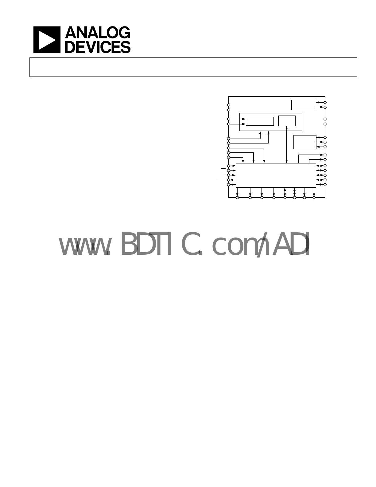
Sigma-Delta ADC
AD7723
FUNCTIONAL BLOCK DIAGRAM
SDO/
DB8
REF2
REF1
DV
DD
DGND
XTAL_OFF
XTAL
CLKIN
DGND/DB15
DGND/DB14
SCR/DB13
SLDR/DB12
SLP/DB11
TSI/DB10
FSO/DB9
FIR
FSI/
DB6
2.5V
REFERENCE
XTAL
CLOCK
SCO/
DB7
AV
AGND
VIN(+)
VIN(–)
UNI
HALF_PWR
STBY
MODE 1
MODE 2
SYNC
DVDD/CS
CFMT/RD
DGND/DRDY
DGND/DB0
DGND/
DB1
AD7723
MODULATOR
DGND/
DGND/
DB2
DB3
CONTROL
LOGIC
DOE/
SFMT/
DB4
Figure 1.
FILTER
DB5
DD
The part provides an on-chip 2.5 V reference. Alternatively, an
external reference can be used.
A power-down mode reduces the idle power consumption
to 200 µW.
The AD7723 is available in a 44-lead MQFP package and is
specified over the industrial temperature range from
–40°C to +85°C.
01186-001
Data can be read from the device in either serial or parallel
format. A stereo mode allows data from two devices to share a
single serial data line. All interface modes offer easy, high speed
connections to modern digital signal processors.
Rev. C
Information furnished by Analog Devices is believed to be accurate and reliable.
However, no responsibility is assumed by Analog Devices for its use, nor for any
infringements of patents or other rights of third parties that may result from its use.
Specifications subject to change without notice. No license is granted by implication
or otherwise under any patent or patent rights of Analog Devices. Trademarks and
registered trademarks are the property of their respective owners.
Two input modes are provided, allowing both unipolar and
bipolar input ranges.
One Technology Way, P.O. Box 9106, Norwood, MA 02062-9106, U.S.A.
Tel: 781.329.4700 www.analog.com
Fax: 781.461.3113 ©2005 Analog Devices, Inc. All rights reserved.
Page 2

AD7723
www.BDTIC.com/ADI
TABLE OF CONTENTS
Specifications..................................................................................... 3
Timing Specifications....................................................................... 6
Absolute Maximum Ratings.......................................................... 10
ESD Caution................................................................................ 10
Pin Configuration And Function Descriptions.......................... 11
Te r mi n ol o g y .................................................................................... 14
Typical Performance Characteristics ........................................... 15
Circuit Description......................................................................... 18
Applying the AD7723 .................................................................... 20
Analog Input Range ................................................................... 20
Analog Input ............................................................................... 20
Driving the Analog Inputs ........................................................ 20
Applying the Reference .............................................................. 21
Clock Generation .......................................................................22
System Synchronization ................................................................ 23
Data Interfacing.............................................................................. 24
Parallel Interface ......................................................................... 24
Serial Interface................................................................................ 25
Two-Channel Multiplexed Operation..................................... 25
Serial Interface to DSPs ................................................................. 27
AD7723 to ADSP-21xx Interface............................................. 27
AD7723 to SHARC Interface.................................................... 27
AD7723 to DSP56002 Interface ............................................... 27
AD7723 to TMS320C5x Interface............................................ 27
Grounding and Layout .................................................................. 28
Outline Dimensions ....................................................................... 29
Ordering Guide .......................................................................... 29
REVISION HISTORY
5/05—Rev. B to Rev. C
Changes to Format ............................................................. Universal
Changes to Figure 6.......................................................................... 8
Changes to System Synchronization............................................ 23
Updated Outline Dimensions....................................................... 29
Changes to the Ordering Guide.................................................... 29
10/03—Rev. A to Rev. B
C
hanges to Ordering Guide............................................................ 8
Outline Dimensions Updated ....................................................... 23
9/02—Data Sheet changed from Rev. 0 to Rev. A
ew TPCs 1 and 2 Added ............................................................. 13
N
Edits to Figures 17 and 18 ............................................................. 18
Outline Dimensions Updated....................................................... 23
Rev. C | Page 2 of 32
Page 3

AD7723
www.BDTIC.com/ADI
SPECIFICATIONS
AVDD = DVDD = 5 V ± 5%; AGND = AGND1 = AGND2 = DGND = 0 V; f
otherwise noted.
Table 1.
B Version
Parameter Test Conditions/Comments Min Typ Max Unit
DYNAMIC SPECIFICATIONS
f
Decimate by 32
Bipolar Mode
Signal to Noise
Full Power 2.5 V reference 87 90 dB
3 V reference 88.5 91 dB
Half Power 86.5 89 dB
Total Harmonic Distortion
Spurious-Free Dynamic Range4 2.5 V reference −92 dB
3 V reference −90 dB
Unipolar Mode
Signal to Noise 87 dB
Total Harmonic Distortion4 −89 dB
Spurious-Free Dynamic Range4 −90 dB
Band-Pass Filter Mode
Bipolar Mode
Signal to Noise 76 79 dB
Decimate by 16
Bipolar Mode
Signal to Noise Measurement bandwidth = 0.383 × F
2.5 V reference 82 86 dB
3 V reference 83 87 dB
Signal to Noise Measurement bandwidth = 0.5 × F
Total Harmonic Distortion4 2.5 V reference −88 dB
Spurious-Free Dynamic Range4 3 V reference −86 dB
2.5 V reference −90 dB
3 V reference −88 dB
Unipolar Mode
Signal to Noise Measurement bandwidth = 0.383 × F
Signal to Noise Measurement bandwidth = 0.5 × F
Total Harmonic Distortion4 −89 dB
DIGITAL FILTER RESPONSE
Low-Pass Decimate by 32
0 kHz to f
f
/66.9 −3 dB
CLKIN
f
/64 −6 dB
CLKIN
f
/51.9 to f
CLKIN
Group Delay 1293/2 f
Settling Time 1293/f
/83.5 ±0.001 dB
CLKIN
CLKIN
1
= 19.2 MHz; REF2 = 2.5 V; TA = T
CLKIN
2, 3
4
HALF_PWR = 0 to 1
= 10 MHz when HALF_PWR = 1
CLKIN
−96 −90 dB
O
O
O
78 81.5 dB
84 dB
O
81 dB
/2 −90 dB
CLKIN
to T
MIN
CLKIN
MAX
, unless
Rev. C | Page 3 of 32
Page 4

AD7723
www.BDTIC.com/ADI
B Version
Parameter Test Conditions/Comments Min Typ Max Unit
Low-Pass Decimate by 16
0 kHz to f
f
/33.45 −3 dB
CLKIN
f
/32 −6 dB
CLKIN
f
/25.95 to f
CLKIN
Group Delay 541/2 f
Settling Time 541/f
Band-Pass Decimate by 32
f
/51.90 to f
CLKIN
f
/62.95, f
CLKIN
f
/64, f
CLKIN
0 kHz to f
Group Delay 1293/2 f
Settling Time 1293/f
Output Data Rate, F
Decimate by 32 f
Decimate by 166 f
ANALOG INPUTS
Full-Scale Input Span VIN(+) − VIN(−)
Bipolar Mode ±4/5 × V
Unipolar Mode 0 8/5 × V
Absolute Input Voltage VIN(+) − VIN(−) AGND AV
Input Sampling Capacitance 2 pF
Input Sampling Rage, f
CLOCK
CLKIN Duty Ratio 45 55 %
REFERENCE
REF1 Output Resistance 3 kΩ
Using Internal Reference
REF2 Output Voltage 2.39 2.54 2.69 V
REF2 Output Voltage Drift 60 ppm/°C
Using External Reference
REF2 Input Impedance REF1 = AGND 4 kΩ
REF2 External Voltage Range 1.2 2.5 3.15 V
STATIC PERFORMANCE
Resolution 16 Bits
Differential Nonlinearity Guaranteed monotonic ±0.5 ±1 LSB
Integral Nonlinearity ±2 LSB
DC CMRR 80 dB
Offset Error ±20 mV
Gain Error
LOGIC INPUTS (EXCLUDING CLKIN)
V
, Input High Voltage 2.0 V
INH
V
, Input High Voltage 0.8 V
INL
CLOCK INPUT (CLKIN)
V
, Input High Voltage 3.8 V
INH
V
, Input High Voltage 0.4 V
INL
ALL LOGIC INPUTS
IIN, Input Current VIN = 0 V to DV
CIN, Input Capacitance 10 pF
/41.75 ±0.001 dB
CLKIN
/2 −90 dB
CLKIN
CLKIN
CLKIN
/41.75 ±0.001 dB
CLKIN
/33.34 −3 dB
CLKIN
/32 −6 dB
CLKIN
/83.5, f
CLKIN
5
O
/25.95 to f
CLKIN
CLKIN
/2 −90 dB
CLKIN
CLKIN
/32
CLKIN
/16
CLKIN
19.2 MHz
±0.5 % FSR
DD
±10 µA
CLKIN
REF2
REF2
DD
V
V
V
Rev. C | Page 4 of 32
Page 5

AD7723
www.BDTIC.com/ADI
B Version
Parameter Test Conditions/Comments Min Typ Max Unit
LOGIC OUPUTS
VOH, Output High Voltage |I
VOL, Output Low Voltage |I
POWER SUPPLIES
AV
DD
I
AVDD
HALF_PWR = Logic High 25 33 mA
DV
DD
I
DVDD
HALF_PWR = Logic High 15 20 mA
Power Consumption
1
Operating temperature range is −40°C to +85°C (B: Version).
2
Typical values for SNR apply for parts soldered directly to the PCB ground plane.
3
Dynamic specifications apply for input signal frequencies from dc to 0.0240 × f
4
When using the internal reference, THD and SFDR specifications apply only to input signals above 10 kHz with a 10 µF decoupling capacitor between REF2 and
AGND2. At frequencies below 10 kHz, THD degrades to 84 dB and SFDR degrades to 86 dB.
5
Gain error excludes reference error.
6
CLKIN and digital inputs static and equal to 0 or DVDD.
6
| = 200 µA 4.0 V
OUT
| = 1.6 mA 0.4 V
OUT
4.75 5.25 V
HALF_PWR = Logic Low 50 60 mA
4.75 5.25 V
HALF_PWR = Logic Low 25 35 mA
Standby Mode 200 µW
in decimate by 16 mode and from dc to 0.0120 × f
CLKIN
in decimate by 32 mode.
CLKIN
Rev. C | Page 5 of 32
Page 6
AD7723
www.BDTIC.com/ADI
TIMING SPECIFICATIONS
AVDD = DVDD = 5 V ± 5%; AGND = AGND1 = DGND = 0 V; f
or high; T
A
= T
MIN
to T
, unless otherwise noted.
MAX
Table 2.
Parameter Symbol Min Typ Max Unit
CLKIN Frequency f
CLKIN Period (t
CLK
– 1/f
) t
CLK
CLKIN Low Pulse Width t
CLKIN High Pulse Width t
CLKIN Rise Time t
CLKIN Fall Time t
FSI Setup Time t
FSI Hold Time t
FSI High Time
1
CLKIN to SCO Delay t
SCO Period2, SCR = 1 t
SCO Period2, SCR = 0 t
SCO Transition to FSO High Delay t
SCO Transition to FSO Low Delay t
SCO Transition to SDO Valid Delay t
SCO Transition from FSI
3
SDO Enable Delay Time t
SDO Disable Delay Time t
DRDY
High Time2
Conversion Time2 (Refer to Table 3 and Table 4) t
CLKIN to
DRDY
Transition
CLKIN to DATA Valid t
CS
/RD Setup Time to CLKIN
CS
/RD Hold Time to CLKIN
Data Access Time t
Bus Relinquish Time t
SYNC Input Pulse Width t
SYNC Low Time before CLKIN Rising t
DRDY
High Delay after Rising SYNC
DRDY
Low Delay after SYNC Low
1
FSO pulses are gated by the release of FSI (going low).
2
Guaranteed by design.
3
Frame sync is initiated on the falling edge of CLKIN.
= 19.2 MHz; CL = 50 pF; SFMT = logic low or high, CFMT = logic low
CLKIN
CLK
1
2
3
4
5
6
7
t
8
9
10
10
11
12
13
t
14
15
16
t
17
18
t
19
20
t
21
t
22
23
24
25
26
t
27
t
28
1 19.2 MHz
0.052 1 µs
0.45 × t
0.45 × t
1
1
0.55 × t
0.55 × t
1
1
5 ns
5 ns
0 5 ns
0 5 ns
1 t
25 40 ns
2 t
1 t
0 5 ns
0 5 ns
5 12 ns
60 t
CLK
+ t
2
5 20 ns
5 20 ns
2 t
16/32 t
35 50 ns
20 35 ns
0 ns
20 ns
20 35 ns
20 35 ns
1 t
0 ns
25 35 ns
2049 t
CLK
CLK
CLK
CLK
CLK
CLK
CLK
I
OL
1.6mA
TO
OUTPUT
PIN
50pF
C
L
I
OH
200µA
1.6V
01186-002
Figure 2. Load Circuit for Timing Specifications
Rev. C | Page 6 of 32
Page 7
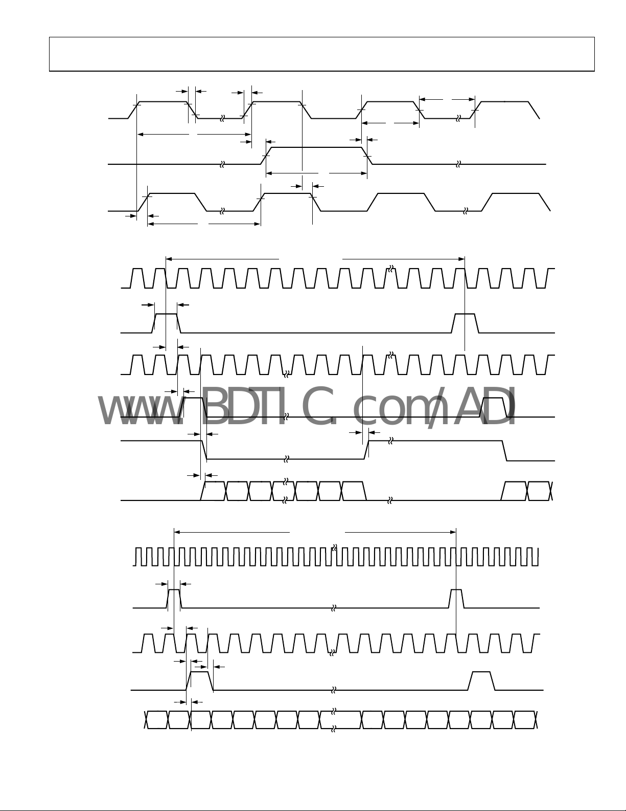
AD7723
www.BDTIC.com/ADI
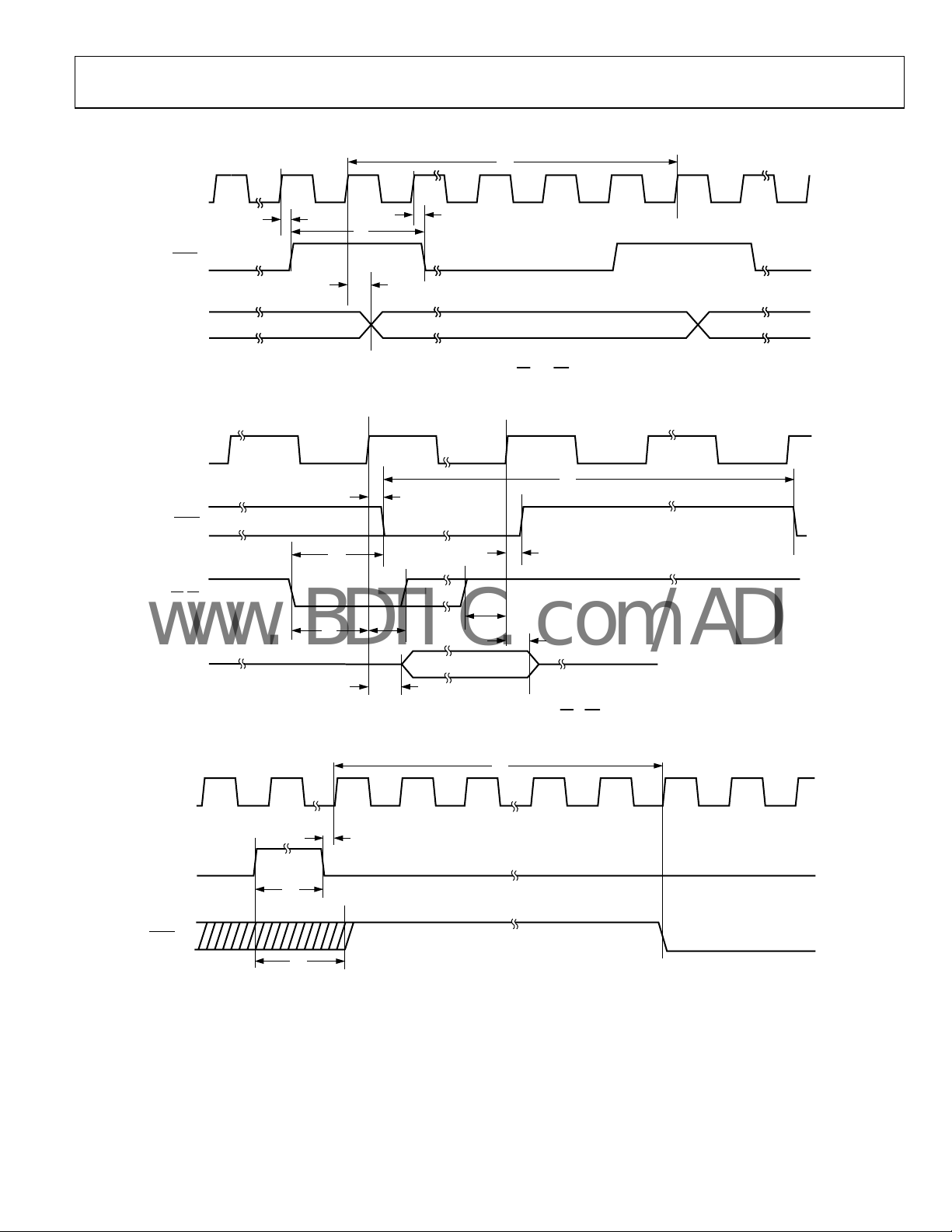
t
CLKIN
FSI
SCO
CLKIN
FSI
(SFMT = 1)
SCO
(CFMT = 0)
2.3V
5
0.8V
t
1
t
9
t
10
Figure 3. Serial Mode Timing for Clock Input, Frame Sync Input, and Serial Clock Output
t
8
t
14
t
4
t
6
t
8
t
9
32 CLKIN CYCLES
t
2
t
3
t
7
01186-003
t
11
FSO
(SFMT = 0)
t
11
01186-004
FSO
(SFMT = 1)
SDO
t
12
t
13
D15 D14 D13 D2 D1 D0 D15 D14
Figure 4. Serial Mode 1: Timing for Frame Sync Input, Frame Sync Output, Serial Clock Output, and Serial Data Output (See Table 3 for Control Inputs, TSI = DOE)
32 CLKIN CYCLES
CLKIN
t
8
FSI
t
SCO
(CFMT = 0)
FSO
14
t
11
t
12
t
13
SDO
D2 D1 D0 D15 D14 D13 D12 D11 D5
D3 D2 D1 D0 D15 D14
D4
Figure 5. Serial Mode 2: Timing for Frame Sync Input, Frame Sync Output, Serial Clock Output, and Serial Data Output (See Table 3 for Control Inputs, TSI = DOE)
Rev. C | Page 7 of 32
01186-005
Page 8
AD7723
www.BDTIC.com/ADI
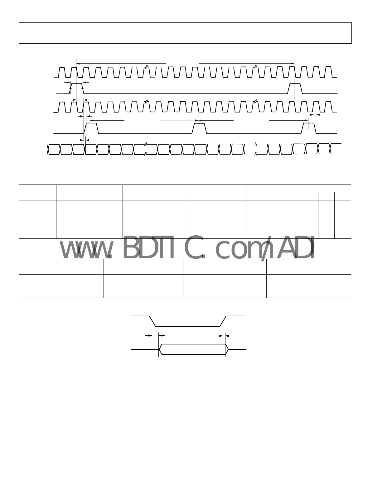
32 CLKIN CYCLES
CLKIN
t
FSI
SCO
(CFMT = 0)
FSO
SDO
t
t
13
D3
D2
8
t
14
t
D15
12
01186-006
11
D1
D15D0
16 CLKIN CYCLES 16 CLKIN CYCLES
D14
D13 D13 D3
D2
D3
D0D1
D15 D14 D1D2 D0
Figure 6. Serial Mode 3: Timing for Frame Sync Input, Frame Sync Output, Serial Clock Output, and Serial Data Output (See Table 3 for Control Inputs, TSI = DOE)
Table 3. Serial Interface (MODE1 = 0, MODE2 = 0)
Control Inputs
Serial Mode Decimation Ratio (SLDR) Digital Filter Mode (SLP) SCO Frequency (SCR) Output Data Rate SLDR SLP SCR
1 32 Low Pass f
1 32 Band Pass f
2 32 Low Pass f
2 32 Band Pass f
3 16 Low Pass f
CLKIN
CLKIN
/2 f
CLKIN
/2 f
CLKIN
CLKIN
f
/32 1 1 0
CLKIN
f
/32 1 0 0
CLKIN
/32 1 1 1
CLKIN
/32 1 0 1
CLKIN
f
/16 0 1 0
CLKIN
Table 4. Parallel Interface
Control Inputs
Digital Filter Mode Decimation Ratio Output Data Rate MODE1 MODE2
Band Pass 32 f
Low Pass 32 f
Low Pass 16 f
/32 0 1
CLKIN
/32 1 0
CLKIN
/16 1 1
CLKIN
DOE
t
16
01186-007
SDO
t
15
Figure 7. Serial Mode Timing for Data Output Enable and Serial Data Output
Rev. C | Page 8 of 32
Page 9
AD7723
www.BDTIC.com/ADI
t
18
CLKIN
t
19
DRDY
t
19
t
17
t
20
DB0–DB15
CLKIN
DRDY
RD/CS
DB0–DB15
WORD N – 1 WORD N + 1
Figure 8. Parallel Mode Read Timing,
WORD N
CS
and RD Tied Logic Low
t
18
t
19
t
22
t
t
t
21
22
t
23
21
VALID DATA
Figure 9. Parallel Mode Read Timing,
t
19
t
24
CS
= RD
t
28
01186-008
01186-009
CLKIN
t
26
SYNC
t
25
DRDY
t
27
Figure 10. SYNC Timing
Rev. C | Page 9 of 32
01186-010
Page 10

AD7723
www.BDTIC.com/ADI
ABSOLUTE MAXIMUM RATINGS
TA = 25°C, unless otherwise noted.
Table 5.
Parameter Rating
DVDD to DGND −0.3 V to +7 V
AVDD, AV
AVDD, AV
AGND, AGND1 to DGND
Digital Inputs to DGND −0.3 V to DVDD + 0.3 V
Digital Outputs to DGND −0.3 V to DVDD + 0.3 V
VIN (+), VIN(−) to AGND −0.3 V to AVDD + 0.3 V
REF1 to AGND −0.3 V to AVDD + 0.3 V
REF2 to AGND −0.3 V to AVDD + 0.3 V
Operating Temperature Range −40°C to +85°C
Storage Temperature Range −65°C to +150°C
Junction Temperature 150°C
θJA Thermal Impedance
Lead Temperature, Soldering
Vapor Phase (60 sec) 215°C
Infrared (15 sec) 220°C
to AGND −0.3 V to +7 V
DD1
DD1
to DV
DD
−1 V to +1 V
−0.3 V to +0.3 V
95°C/W
Stresses above those listed under Absolute Maximum Ratings
may cause permanent damage to the device. This is a stress
rating only; functional operation of the device at these or any
other conditions above those indicated in the operational
section of this specification is not implied. Exposure to absolute
maximum rating conditions for extended periods may affect
device reliability.
ESD CAUTION
ESD (electrostatic discharge) sensitive device. Electrostatic charges as high as 4000 V readily accumulate
on the human body and test equipment and can discharge without detection. Although this product features
proprietary ESD protection circuitry, permanent damage may occur on devices subjected to high energy
electrostatic discharges. Therefore, proper ESD precautions are recommended to avoid performance
degradation or loss of functionality.
Rev. C | Page 10 of 32
Page 11

AD7723
www.BDTIC.com/ADI
PIN CONFIGURATION AND FUNCTION DESCRIPTIONS
DD
FSI/DB6
SCO/DB7
DV
40 39 3841
AD7723
TOP VIEW
(Not to Scale)
DD
AV
AGND
HALF_PWR
SDO/DB8
AGND
FSO/DB9
VIN(–)
TSI/DB10
SLP/DB11
SLDR/DB12
33
SCR/DB13
32
DGND/DB14
31
DGND/DB15
30
DVDD/CS
29
SYNC
28
DGND
27
STBY
26
AV
DD
25
AGND
24
UNI
23
REF2
REF1
VIN(+)
AGND2
01186-011
DGND/DB2
DGND/DB1
DGND/DB0
CFMT/RD
DGND/DRDY
DGND
MODE2
MODE1
AGND1
AGND1
AV
DD1
DOE/DB4
DGND/DB3
SFMT/DB5
42
4344 3 6 35 3437
1
PIN 1
IDENTIFIER
2
3
4
5
6
7
8
9
10
11
12 13 14 15 16 17 18 192021 22
XTAL
CLKIN
XTAL_OFF
Figure 11. 44-Lead MQFP
Table 6. Pin Function Descriptions
Pin No. Mnemonic Description
6, 28 DGND Ground Reference for Digital Circuitry.
8, 7 MODE1/MODE2
Mode Control Inputs. The MODE1 and MODE2 pins choose either parallel or serial data interface operation
and select the operating mode for the digital filter in parallel mode. See Table 3 and Table 4.
9, 10 AGND1 Digital Logic Power Supply Ground for the Analog Modulator.
11 AV
DD1
12 CLKIN
Digital Logic Power Supply Voltage for the Analog Modulator.
Clock Input. An external clock source can be applied directly to this pin with XTAL_OFF tied high.
Alternatively, a parallel resonant fundamental frequency crystal, in parallel with a 1 MΩ resistor, can
be connected betweenthe XTAL pin and the CLKIN pin with XTAL_OFF tied low. External capacitors
are then required from the CLKIN and XTAL pins to ground. Consult the crystal manufacturer’s
recommendation for the load capacitors.
13 XTAL Input to Crystal Oscillator Amplifier. If an external clock is used, XTAL should be tied to AGND1.
14 XTAL_OFF
Oscillator Enable Input. A logic high disables the crystal oscillator amplifier to allow use of an external
clock source. Set low when using an external crystal between the CLKIN and XTAL pins.
15 HALF_PWR
When set high, the power dissipation is reduced by approximately one-half, and a maximum CLKIN
frequency of 10 MHz applies.
16, 18, 25 AGND Power Supply Ground for the Analog Modulator.
17, 26 AV
DD
Positive Power Supply Voltage for the Analog Modulator.
19 VIN(−) Negative Terminal of the Differential Analog Input.
20 VIN(+) Positive Terminal of the Differential Analog Input.
21 REF1
Reference Output. REF1 connects through 3 kΩ to the output of the internal 2.5 V reference and to a buffer
amplifier that drives the Σ-∆ modulator.
22 AGND2 Power Supply Ground Return to the Reference Circuitry, REF2, of the Analog Modulator.
23 REF2
Reference Input. REF2 connects to the output of an internal buffer amplifier that drives the Σ-∆ modulator.
When REF2 is used as an input, REF1 must be connected to AGND to disable the internal buffer amplifier.
24 UNI
Analog Input Range Select Input. The UNI pin selects the analog input range for either bipolar or unipolar
operation. A logic high input selects unipolar operation and a logic low selects bipolar operation.
27 STBY Standby Logic Input. A logic high sets the AD7723 into the power-down state.
Rev. C | Page 11 of 32
Page 12

AD7723
www.BDTIC.com/ADI
Pin No. Mnemonic Description
29 SYNC
39 DV
Table 7. Parallel Mode Pin Function Descriptions
Pin
No. Mnemonic Description
1 DGND/DB2 Data Output Bit.
2 DGND/DB1 Data Output Bit.
3 DGND/DB0 Data Output Bit (LSB).
4
CFMT/RD
5
DGND/DRDY
30
DV
31 DGND/DB15 Data Output Bit (MSB).
32 DGND/DB14 Data Output Bit.
33 SCR/DB13 Data Output Bit.
34 SLDR/DB12 Data Output Bit.
35 SLP/DB11 Data Output Bit.
36 TSI/DB10 Data Output Bit.
37 FSO/DB9 Data Output Bit.
38 SDO/DB8 Data Output Bit.
40 SCO/DB7 Data Output Bit.
41 FSI/DB6 Data Output Bit.
42 SFMT/DB5 Data Output Bit.
43 DOE/DB4 Data Output Bit.
44 DGND/DB3 Data Output Bit.
DD
Read Logic Input. Used in conjunction with CS to read data from the parallel bus. The output data bus is enabled
when the rising edge of CLKIN senses a logic low level on RD
data bits, DB15 to DB0, are high impedance.
Data Ready Logic Output. A falling edge indicates a new output word is available to be read from the output data
register. DRDY returns high upon completion of a read operation. If a read operation does not occur between output
updates, DRDY pulses high for two CLKIN cycles before the next output update. DRDY also indicates when
conversion results are available after a SYNC sequence.
DD
/CS
Chip Select Logic Input.
Synchronization Logic Input. When using more than one AD772
SYNC allows each ADC to simultaneously sample its analog input and update its output register. A rising
edge resets the AD7723 digital filter sequencer counter to 0. When the rising edge of CLKIN senses a logic
low on SYNC, the reset state is released. Because the digital filter and sequencer are completely reset
during this action, SYNC pulses cannot be applied continuously.
Digital Power Supply Voltage; 5 V ± 5%.
3 operated from a common master clock,
if CS is also low. When RD is sensed high, the output
Rev. C | Page 12 of 32
Page 13

AD7723
www.BDTIC.com/ADI
Table 8. Serial Mode Pin Function Descriptions
Pin
No.
Mnemonic Description
1 DGND/DB2 Tie to DGND.
2 DGND/DB1 Tie to DGND.
3 DGND/DB0 Tie to DGND.
4
CFMT/RD
5
DGND/DRDY
30
DV
31 DGND/DB15 Tie to DGND.
32 DGND/DB14 Tie to DGND.
33 SCR/DB13
34 SLDR/DB12
35 SLP/DB11
36 TSI/DB10
37 FSO/DB9
38 SDO/DB8
40 SCO/DB7 Serial Clock Output.
41 FSI/DB6
42 SFMT/DB5
43 DOE/DB4
44 DGND/DB3 Tie to DGND.
Serial Clock Format Logic Input. The clock format pin selects whether the serial data, SDO, is valid on the rising or
falling edge of the serial clock, SCO. When CFMT is logic low, serial data is valid on the falling edge of the serial clock,
SCO. If CFMT is logic high, SDO is valid on the rising edge of SCO.
Tie to DGND.
/CS
DD
Tie to DVDD.
Serial Clock Rate Select Input. With SCR set logic low, the ser
frequency. A logic high sets it equal to one-half the CLKIN frequency.
Serial Mode Low/High Output Data Rate Select Input. With SLD
low selects the high data rate. The high data rate corresponds to data at the output of the fourth decimation filter
(decimate by 16). The low data rate corresponds to data at the output of the fifth decimation filter (decimate by 32).
Serial Mode Low-Pass/Band-Pass Filter Select Input. With SLP s
A logic low selects band-pass.
Time Slot Logic Input. The logic level on TSI sets the active state of the DOE pin. With TSI set logic high, DOE enables
the SDO output
same serial data bus. When this function is not needed, TSI and DOE should be tied low.
Frame Sync Output. FSO indicates the beginning of a word transmission on the SDO pin. Depending on the logic
level of the SFMT pin, the FSO signal is either a p
that is active low for the duration of the 16-data bit transmission.
Serial Data Output. The serial data is shifted out
transmissions last 32 SCO cycles. After the LSB is output, trailing zeros are output for the remaining 16 SCO cycles.
Serial Modes 2 and 3 data transmissions last 16 SCO cycles.
Frame Synchronization Logic Input. The FSI input is used to synchronize the AD7723 serial output data register to an
external
sample its analog input and update its output register.
Serial Data Format Logic Input. The logic level
A logic low makes the FSO output a pulse one SCO cycle wide at the beginning of a serial data transmission. With
SFMT set to a logic high, the FSO signal is a frame pulse that is active low for the duration of the 16-bit transmission.
For Serial Modes 2 and 3, SFMT should be tied high.
Data Output Enable Logic Input. The DOE pin controls the three-state output buf
of DOE is determined by the logic level on the TSI pin. When the DOE logic level equals the level on the TSI pin, the
serial data output, SDO, is active. Otherwise, SDO is high impedance. SDO can be three-state after a serial data
transmission by connecting DOE to FSO. In normal operations, TSI and DOE should be tied low.
buffer when it is a logic high and vice versa. TSI is used when two AD7723s are connected to the
ositive pulse approximately one SCO period wide or a frame pulse
MSB first, synchronous with the SCO. Serial Mode 1 data
source and to allow more than one AD7723, operated from a common master clock, to simultaneously
on the SFMT pin selects the format of the FSO signal for Serial Mode 1.
ial clock output frequency, SCO, is equal to the CLKIN
R set logic high, the low data rate is selected. A logic
et logic high, the low-pass filter response is selected.
fer of the SDO pin. The active state
Rev. C | Page 13 of 32
Page 14

AD7723
www.BDTIC.com/ADI
TERMINOLOGY
Signal-to-Noise Ratio (SNR)
SNR is the measured signal-to-noise ratio at the output of the
ADC. The signal is the rms magnitude of the fundamental.
Noise is the rms sum of all of the nonfundamental signals up to
half the output data rate (F
evaluated by applying a low noise, low distortion sine wave
signal to the input pins. By generating a fast fourier transform
(FFT) plot, the SNR data can then be obtained from the output
spectrum.
/2), excluding dc. The ADC is
O
Integral Nonlinearity
This is the maximum deviation of any code from a straight line
passing through the endpoints of the transfer function. The
endpoints of the transfer function are minus full scale, a point
0.5 LSB below the first code transition (100 . . . 00 to 100 . . . 01
in bipolar mode, 000 . . . 00 to 000 . . . 01 in unipolar mode),
and plus full scale, a point 0.5 LSB above the last code transition
(011 . . . 10 to 011 . . . 11 in bipolar mode, 111 . . . 10 to 111 . . .
11 in unipolar mode). The error is expressed in LSBs.
Total Harmonic Distortion (THD)
THD is the ratio of the rms sum of the harmonics to the rms
value of the fundamental. THD is defined as
2
THD
= 20log
V
where
V
is the rms amplitude of the fundamental, and V2, V3,
1
, V5, and V6 are the rms amplitudes of the second through
4
2
4
3
V
1
VVVVV
++++
6
5
2
2
2
2
sixth harmonics. The THD is also derived from the FFT plot of
the ADC output spectrum.
Spurious-Free Dynamic Range (SFDR)
Defined as the difference, in dB, between the peak spurious or
harmonic component in the ADC output spectrum (up to F
/2
O
and excluding dc) and the rms value of the fundamental.
Normally, the value of this specification is determined by the
largest harmonic in the output spectrum of the FFT. For input
signals whose second harmonics occur in the stop-band region
of the digital filter, the spur in the noise floor limits the SFDR.
Pass-Band Ripple
The frequency response variation of the AD7723 in the defined
pass-band frequency range.
Pass-Band Frequency
The frequency up to which the frequency response variation is
within the pass-band ripple specification.
Cutoff Frequency
The frequency below which the AD7723’s frequency response
will not have more than 3 dB of attenuation.
Differential Nonlinearity
This is the difference between the measured and the ideal 1 LSB
change between two adjacent codes in the ADC.
Common-Mode Rejection Ratio
The ability of a device to reject the effect of a voltage applied to
both input terminals simultaneously—often through variation
of a ground level—is specified as a common–mode rejection
ratio. CMRR is the ratio of gain for the differential signal to the
gain for the common-mode signal.
Unipolar Offset Error
Unipolar offset error is the deviation of the first code transition
(10 . . . 000 to 10 . . . 001) from the ideal differential voltage
(VIN(+) – VIN(–)+ 0.5 LSB) when operating in the unipolar
mode.
Bipolar Offset Error
This is the deviation of the midscale transition code (111 . . . 11
to 000 . . . 00) from the ideal differential voltage (VIN(+) –
VIN(–) – 0.5 LSB) when operating in the bipolar mode.
Gain Error
The first code transition should occur at an analog value ½ LSB
above –full scale. The last transition should occur for an analog
value 1 ½ LSB below the nominal full scale. Gain error is the
deviation of the actual difference between first and last code
transitions and the ideal difference between first and last code
transitions.
Stop-Band Frequency
The frequency above which the AD7723’s frequency response
will be within its stop-band attenuation.
Stop-Band Attenuation
The AD7723’s frequency response will not have less than 90 dB
of attenuation in the stated frequency band.
Rev. C | Page 14 of 32
Page 15

AD7723
www.BDTIC.com/ADI
TYPICAL PERFORMANCE CHARACTERISTICS
AVDD = DVDD = 5 V; TA = 25°C; CLKIN = 19.2 MHz; external 2.5 V reference, unless otherwise noted.
110
SIGNAL FREQUENCY = 98kHz
MEASUREMENT BANDWIDTH = 460kHz
100
90
80
(dB)
70
60
50
40
–50 –40
THD
SFDR
SNR
–30 –20 –10 0
ANALOG INPUT LEVEL (dB)
01186-012
Figure 12. SNR, THD, and SFDR vs. Analog Input Level Relative to Full Scale
(Output Data Rate = 1.2 MHz)
110
SIGNAL FREQUENCY = 98kHz
MEASUREMENT BANDWIDTH = 300kHz
100
90
80
(dB)
70
60
50
40
–50 0–40
THD
SFDR
SNR
–30 –20
ANALOG INPUT LEVEL (dB)
–10
01186-013
Figure 13. SNR, THD, and SFDR vs. Analog Input Level Relative to Full Scale
(Output Data Rate = 600 kHz)
102
SIGNAL FREQUENCY = 98kHz
MEASUREMENT BANDWIDTH = 460kHz
100
(dB)
98
96
94
92
90
88
86
84
–50
TEMPERATURE (°C)
3RD
2ND
THD
SNR
100–25 0 25 50 75
01186-014
Figure 14. SNR and THD vs. Temperature (Output Data Rate = 1.2 MHz)
106
SIGNAL FREQUENCY = 98kHz
MEASUREMENT BANDWIDTH = 300kHz
104
102
100
98
(dB)
96
94
92
90
88
–50
TEMPERATURE (°C)
3RD
2ND
THD
SNR
01186-015
100–25 0 25 50 75
Figure 15. SNR and THD vs. Temperature (Output Data Rate = 600 kHz)
106
104
102
100
98
96
(dB)
INPUT SIGNAL = 10kHz
94
MEASUREMENT BANDWIDTH = 0.383 × OWR
92
90
88
86
84
100 500
SFDR
1000 1500 2150
OUTPUT WORD RATE (kHz)
THD
SNR
01186-016
Figure 16. SNR, THD, and SFDR vs. Sampling Frequency (Decimate by 16)
115
INPUT SIGNAL = 10kHz
MEASUREMENT BANDWIDTH = 0.5 × OWR
110
105
(dB)
100
95
90
50 150
300 600 900
OUTPUT WORD RATE (kHz)
450 750
SFDR
THD
SNR
01186-017
Figure 17. SNR, THD, and SFDR vs. Sampling Frequency (Decimate by 32)
Rev. C | Page 15 of 32
Page 16

AD7723
G
www.BDTIC.com/ADI
2000
VIN(+) = VIN(–)
1800
8192 SAMPLES TAKEN
1600
1400
1200
1000
800
600
400
FREQUENCY OF OCCURRENCE
200
0
32700 3271332702
Figure 18. Histogram of Output Codes with DC Input
5000
VIN(+) = VIN(–)
4500
8192 SAMPLES TAKEN
4000
3500
3000
2500
2000
1500
1000
FREQUENCY OF OCCURRENCE
500
0
32703 3271032704
Figure 19. Histogram of Output Codes with DC Input
1.0
67108864 SAMPLES TAKEN
0.8
DIFFERENTIAL MODE
0.6
0.4
0.2
0
–0.2
DNL ERROR (LSB)
–0.4
–0.6
–0.8
–1.0
0
Figure 20. Differential Nonlinearity (Output Data Rate = 1.2 MHz)
32704 32706 32708 32710 32712
CODE
(Output Data Rate = 1.2 MHz)
32705 32706 32707 32708 32709
CODE
(Output Data Rate = 600 kHz)
CODE
R
FB
R
IN
390Ω
SOURCE
FB
220Ω
AD8047
A1
R
BALANCE2
220Ω
R
BALANCE2
220Ω
A2
AD8047
)/(2 × RFB)
27Ω
27Ω
20
VIN(+)
220pF
AD7723
19
VIN(–)
23
10nF220nF
1µF
REF2
21
REF1
01186-021
01186-018
AIN = ±2V
BIASED
ABOUT
GROUND
AIN = 2 × RFB/(RIN + R
R
= R
BALANCE1
R
REF2
= R
REF1
BALANCE2
× (RIN + R
R
SOURCE
R
10kΩ
SOURCE
× (RIN + R
SOURCE
50Ω
R
BALANCE1
220Ω
REF1
R
REF2
20kΩ
)
)/R
Figure 21. Differential Nonlinearity (Output Data Rate = 600 kHz)
1.0
67108864 SAMPLES TAKEN
DIFFERENTIAL MODE
0.8
0.6
0.4
0.2
0
–0.2
INL ERROR (LSB)
–0.4
–0.6
–0.8
01186-019
–1.0
0
CODE
01186-022
6553516384 32768 49152
Figure 22. Integral Nonlinearity (Output Data Rate =1.2 MHz)
1.0
67108864 SAMPLES TAKEN
DIFFERENTIAL MODE
0.8
0.6
0.4
0.2
0
–0.2
INL ERROR (LSB)
–0.4
–0.6
–0.8
01186-020
6553516384 32768 49152
–1.0
0
CODE
01186-023
6553516384 32768 49152
Figure 23. Integral Nonlinearity (Output Data Rate = 600 kHz)
Rev. C | Page 16 of 32
Page 17

AD7723
www.BDTIC.com/ADI
225
200
175
150
125
100
POWER (mW)
75
50
25
AIDD(HALF_POWER = 1)
0
02
AIDD(HALF_POWER = 0)
DI
DD
5101520
CLOCK FREQUENCY (MHz)
01186-024
5
Figure 24. Power Consumption vs. CLKIN Frequency
0
SNR = –86.19dB
–25
–50
–75
SNR + D = –85.9dB
THD = –96.42dB
SFDR = –99.61dB
2ND HARMONIC = –100.98dB
3RD HARMONIC = –99.61dB
A
= 100kHz
IN
MEASURED BW = 460kHz
0
–20
–40
–60
–80
–100
–120
–140
POWER LEVEL RELATIVE TO FULL SCALE (dB)
–160
0
50k 100k
SNR = –89.91dB
SNR + D = –89.7dB
THD = –101.16dB
SFDR = –102.1dB
2ND HARMONIC = –102.1dB
3RD HARMONIC = –110.3dB
A
= 50kHz
IN
MEASURED BW = 300kHz
150k 200k 250k
FREQUENCY (Hz)
Figure 26. 16 K Point FFT (Output Data Rate = 600 kHz)
300k
01186-026
–100
–125
POWER LEVEL RELATIVE TO FULL SCALE (dB)
–150
0
100k 200k
300k 400k 500k
FREQUENCY (Hz)
Figure 25. 16 K Point FFT (Output Data Rate = 1.2 MHz)
01186-025
600k
Rev. C | Page 17 of 32
Page 18

AD7723
www.BDTIC.com/ADI
CIRCUIT DESCRIPTION
The AD7723 ADC employs a Σ-Δ conversion technique to
convert the analog input into an equivalent digital word. The
modulator samples the input waveform and outputs an
equivalent digital word at the input clock frequency, f
Due to the high oversampling rate that spreads the quantization
noise from 0 to f
/2, the noise energy contained in the band
CLKIN
of interest is reduced (Figure 27A). To further reduce the
quantization noise, a high-order modulator is employed to
shape the noise spectrum so that most of the noise energy is
shifted out of the band of interest (Figure 27B).
The digital filter that follows the modulator removes the large
out-of-band quantization noise (Figure 27C) while also
reducing the data rate from f
f
CLKIN
/32 or f
/16 at the output of the filter, depending on the
CLKIN
at the input of the filter to
CLKIN
state on the MODE1/MODE2 pins in parallel interface mode or
the SLDR pin in serial interface mode. The AD7723 output data
rate is a little over twice the signal bandwidth, which guarantees
that there is no loss of data in the signal band.
Digital filtering has certain advantages over analog filtering.
First, since digital filtering occurs after the A/D conversion, it
can remove noise injected during the conversion process.
Analog filtering cannot remove noise injected during
conversion. Second, the digital filter combines low pass-band
ripple with a steep roll-off while also maintaining a linear phase
response.
CLKIN
.
the converter is 16. Data fed to the interface from the output of
the fifth filter results in an output data rate of f
CLKIN
/32 and a
corresponding OSR for the converter of 32. When an output
data rate (ODR) of f
/32 is selected, the digital filter
CLKIN
response can be set to either low-pass or band-pass. The bandpass response is useful when the input signal is band limited
because the resulting output data rate is half that required to
convert the band when the low-pass operating mode is used. To
illustrate the operation of this mode, consider a band-limited
signal, as shown in Figure 28A. This signal band can be
correctly converted by selecting the (low-pass) ODR = f
CLKIN
/16
mode, as shown in Figure 28B. Note that the output data rate is a
little over twice the maximum frequency in the frequency band.
Alternatively, the band-pass mode can be selected, as shown in
Figure 28C. The band-pass filter removes unwanted signals
from dc to just below f
/16, the output of the band-pass filter is sampled at
f
CLKIN
/32. This effectively translates the wanted band to a
f
CLKIN
maximum frequency of a little less than f
/64. Rather than outputting data at
CLKIN
/64, as shown in
CLKIN
Figure 28D. Halving the output data rate reduces the workload
of any following signal processor and also allows a lower serial
clock rate to be used.
0dB
BAND LIMITED SIGNAL
A
f
CLKIN
/16
QUANTIZATION NOISE
f
/2
BAND OF INTEREST
A
NOISE SHAPING
BAND OF INTEREST
B
DIGITAL FILTER CUTOFF FREQUENCY
BAND OF INTEREST
C
Figure 27. Sigma-Delta ADC
CLKIN
f
CLKIN
f
CLKIN
/2
/2
01186-027
The AD7723 employs four or five finite impulse response (FIR)
filters in series. Each individual filter’s output data rate is half
that of the filter’s input data rate. When data is fed to the
interface from the output of the fourth filter, the output data
rate is f
/16 and the resulting oversampling ratio (OSR) of
CLKIN
0dB
LOW-PASS FILTER. OUTPUT DATA RATE = f
BAND-PASS FILTER
0dB
0dB
LOW-PASS FILTER. OUTPUT DATA RATE =
LOW-PASS FILTER RESPONSE
B
RESPONSE
BAND-PASS FILTER
C
FREQUENCY
TRANSLATED
INPUT SIGNAL
Figure 28. Band-Pass Operation
ODR
D
SAMPLE
IMAGE
SAMPLE
IMAGE
SAMPLE
IMAGE
CLKIN
f
CLKIN
f
f
CLKIN
f
CLKIN
ODR
CLKIN
/16
/32
/16
/16
/16
The frequency response of the three digital filter operating
modes is shown in Figure 29, Figure 30, and Figure 31.
01186-028
Rev. C | Page 18 of 32
Page 19

AD7723
–
www.BDTIC.com/ADI
Figure 32 shows the frequency response of the digital filter in
both low-pass and band-pass modes. Due to the sampling
0dB
–100dB
0 1.00.5
Figure 29. Low-Pass Filter Decimate by 16
0dB
100dB
f
CLKIN
01186-029
nature of the converter, the pass-band response is repeated
about the input sampling frequency, f
multiples of f
. Out-of-band noise or signals coincident with
CLKIN
, and at integer
CLKIN
any of the filter images are aliased down to the pass band.
However, due to the AD7723’s high oversampling ratio, these
bands occupy only a small fraction of the spectrum, and most
broadband noise is attenuated by at least 90 dB. In addition, as
shown in Figure 33, with even a low-order filter, there is
significant attenuation at the first image frequency. This
contrasts with a normal Nyquist rate converter where a very
high-order antialias filter is required to allow most of the
bandwidth to be used while ensuring sufficient attenuation at
multiples of f
0dB
OUTPUT
DATA RATE
0dB
.
CLKIN
1f
CLKIN
2f
CLKIN
3f
CLKIN
Figure 32. Digital Filter Frequency Response
ANTIALIAS FILTER
RESPONSE
01186-032
REQUIRED
ATTENUATION
0 1.00.5
Figure 30. Low-Pass Filter Decimate by 32
0dB
–100dB
0 1.00.5
Figure 31. Band-Pass Filter Decimate by 32
f
CLKIN
f
CLKIN
01186-030
01186-031
f
CLKIN
/32
f
CLKIN
01186-033
Figure 33. Frequency Response of Antialias Filter
Rev. C | Page 19 of 32
Page 20

AD7723
www.BDTIC.com/ADI
APPLYING THE AD7723
ANALOG INPUT RANGE
The AD7723 has differential inputs to provide common-mode
noise rejection. In unipolar mode, the analog input range is 0 to
8/5 × V
±4/5 × V
both modes with 1 LSB = 61 µV. The ideal input/output transfer
characteristics for the two modes are shown in Figure 34. In
both modes, the absolute voltage on each input must remain
within the supply range AGND to AV
allows either single-ended or complementary input signals.
011…111
011…110
000…010
000…001
000…000
111…111
111…110
100…001
100…000
The AD7723 accepts full-scale, in-band signals. However, large
scale out-of-band signals can overload the modulator inputs.
Figure 35 shows the maximum input signal level as a function
of frequency. A minimal single-pole, RC, antialias filter set to
f
CLKIN
spectrum.
, while in bipolar mode, the analog input range is
REF2
. The output code is twos complement binary in
REF2
. The bipolar mode
DD
–4/5 × V
(0V)
REF2
0V +4/5 × V
REF2
)
(+4/5 × V
(+8/5 × V
01186-034
– 1LSB BIPOLAR
REF2
– 1LSB) UNIPOLAR
REF2
Figure 34. Bipolar (Unipolar) Mode Transfer Function
/24 allows full-scale input signals over the entire frequency
2.2
2.1
2.0
1.9
1.8
1.7
1.6
PEAK INPUT (V p-p)
1.5
V
= 2.5V
1.4
1.3
REF
0 0.50.02 0.04 0.06 0.08 0.10 0.12 0.14
INPUT SIGNAL FREQUENCY RELATIVE TO
f
CLKIN
Figure 35. Peak Input Signal Level vs. Signal Frequency
01186-035
ANALOG INPUT
The analog input of the AD7723 uses a switched capacitor
technique to sample the input signal. For the purpose of driving
the AD7723, an equivalent circuit of the analog inputs is shown
in Figure 36. For each half clock cycle, two highly linear
sampling capacitors are switched to both inputs, converting the
input signal into an equivalent sampled charge. A signal source
driving the analog inputs must be able to source this charge
while also settling to the required accuracy by the end of each
half-clock phase.
ΦA
500Ω
20
VIN(+)
VIN(–)
500Ω
19
CLKIN
ΦB
ΦA
ΦB
Φ
A
Figure 36. Analog Input Equivalent Circuit
AD7723
2pF
2pF
AC
GROUND
Φ
Φ
Φ
A
B
B
01186-036
DRIVING THE ANALOG INPUTS
To interface the signal source to the AD7723, at least one op
amp is generally required. Choice of op amp is critical to
achieving the full performance of the AD7723. The op amp not
only has to recover from the transient loads that the ADC
imposes on it, but it must also have good distortion
characteristics and very low input noise. Resistors in the signal
path can also add to the overall thermal noise floor,
necessitating the choice of low value resistors.
Placing an RC filter between the drive source and the ADC
inputs, as shown in Figure 37, has a number of beneficial
effects. Transients on the op amp outputs are significantly
reduced because the external capacitor now supplies the
instantaneous charge required when the sampling capacitors are
switched to the ADC input pins and input circuit noise at the
sample images is now significantly attenuated, resulting in
improved overall SNR. The external resistor serves to isolate the
external capacitor from the ADC output, thus improving op
amp stability while also isolating the op amp output from any
remaining transients on the capacitor. By experimenting with
different filter values, the optimum performance can be
achieved for each application. As a guideline, the RC time
constant (R × C) should be less than a quarter of the clock
period to avoid nonlinear currents from the ADC inputs being
stored on the external capacitor and degrading distortion. This
restriction means that this filter cannot form the main antialias
filter for the ADC.
Rev. C | Page 20 of 32
Page 21

AD7723
G
www.BDTIC.com/ADI
R
C
R
VIN(+)
VIN(–)
AD7723
01186-037
Figure 37. Input RC Network
With the unipolar input mode selected, just one op amp is
required to buffer single-ended input signals. However, driving
the AD7723 with complementary signals and with the bipolar
input range selected has some distinct advantages: even-order
harmonics in both the drive circuits and the AD7723 front end
are attenuated and the peak-to-peak input signal range on both
inputs is halved. Halving the input signal range allows some op
amps to be powered from the same supplies as the AD7723.
Although a complementary driver requires the use of two op
amps per ADC, it may avoid the need to generate additional
supplies just for these op amps.
Figure 38 and Figure 39 show two such circuits for driving the
AD7723. Figure 38 is intended for use when the input signal is
biased about 2.5 V, while Figure 39 is used when the input signal
is biased about ground. While both circuits convert the input
signal into a complementary signal, the circuit in Figure 39 also
level shifts the signal so that both outputs are biased about 2.5 V.
Suitable op amps include the AD8047, AD8044, AD8041, and
its dual equivalent, the AD8042. The AD8047 has lower input
noise than the AD8041/AD8042 but has to be supplied from a
+7.5 V/−2.5 V supply. The AD8041/AD8042 typically degrades
SNR from 90 dB to 88 dB but can be powered from the same
single 5 V supply as the AD7723.
R
FB
R
390Ω
/(R
IN
SOURCE
220Ω
AD8047
A1
220Ω
220Ω
A2
AD8047
+ RIN)
27Ω
27Ω
10nF220nF
1µF
220pF
20
19
23
21
VIN(+)
AD7723
VIN(–)
REF2
REF1
R
AIN = ±2V
BIASED
ABOUT 2.5V
SOURCE
50Ω
GAIN = 2 × R
10kΩ
FB
Figure 38. Single-Ended-to-Differential Input Circuit for Bipolar Mode
Operation (Analog Input Biased About 2.5 V)
01186-038
R
FB
AIN = ±2V
BIASED
ABOUT
GROUND
AIN = 2 × RFB/(RIN + R
= R
R
BALANCE1
R
REF2
= R
REF1
BALANCE2
× (RIN + R
R
SOURCE
R
10kΩ
SOURCE
× (RIN + R
SOURCE
50Ω
R
BALANCE1
REF1
R
REF2
20kΩ
)
)/R
220Ω
R
IN
390Ω
SOURCE
FB
220Ω
AD8047
A1
220Ω
R
BALANCE2
R
BALANCE2
220Ω
A2
AD8047
)/(2 × RFB)
27Ω
27Ω
20
VIN(+)
220pF
AD7723
19
VIN(–)
23
10nF220nF
1µF
REF2
21
REF1
01186-039
Figure 39. Single-Ended-to-Differential Input Circuit for Bipolar Mode
Operation (Analog Input Biased About Ground)
APPLYING THE REFERENCE
The reference circuitry used in the AD7723 includes an on-chip
2.5 V band-gap reference and a reference buffer circuit. The
block diagram of the reference circuit is shown in Figure 40.
The internal reference voltage is connected to REF1 through a
3 kΩ resistor and is internally buffered to drive the analog
modulator’s switched cap DAC (REF2). When using the
internal reference, a 1 µF capacitor is required between REF1
and AGND to decouple the band-gap noise. If the internal
reference is required to bias external circuits, use an external
precision op amp to buffer REF1.
1V
REF1
REF2
21
23
1µF
Figure 40. Reference Circuit Block Diagram
Where gain error or gain error drift requires the use of an
external reference, the reference buffer in Figure 40 can be
turned off by grounding the REF1 pin and the external
reference can be applied directly to REF2 pin. The AD7723
accepts an external reference voltage between 1.2 V to 3.15 V.
By applying a 3 V rather than a 2.5 V reference, SNR is typically
improved by about 1 dB. Where the output common-mode
range of the amplifier driving the inputs is restricted, the fullscale input signal span can be reduced by applying a lower than
2.5 V reference. For example, a 1.25 V reference would make
the bipolar input span ±1 V but would degrade SNR.
COMPARATOR
REFERENCE
BUFFER
3kΩ
2.5V
REFERENCE
AD7723
SWITCHED-CAP
DAC REFERENCED
01186-040
Rev. C | Page 21 of 32
Page 22

AD7723
www.BDTIC.com/ADI
In all cases, since the REF2 voltage connects to the analog
modulator, a 220 nF and 10 nF capacitor must connect directly
from REF2 to AGND. The external capacitor provides the
charge required for the dynamic load presented at the REF2 pin
(see Figure 41).
Φ
A
REF2
23
10nF
220nF
CLKIN
Φ
B
A
Figure 41. REF2 Equivalent Input Circuit
The AD780 is ideal to use as an external reference with the
AD7723. Figure 42 shows a suggested connection diagram.
Grounding Pin 8 on the AD780 selects the 3 V output mode.
2.5V
8
7
220nF
6
22µ F
5
1µ F
5V
22nF
1
2
3
4
NC = NO CONNECT
NC
+V
IN
TEMP
GND
SELECT
AD780
O/P
V
OUT
TRIM
NC
Figure 42. External Reference Circuit Connection
CLOCK GENERATION
The AD7723 contains an oscillator circuit to allow a crystal or
an external clock signal to generate the master clock for the
ADC. The connection diagram for use with a crystal is shown
in Figure 43. Consult the manufacturer’s recommendation for
the load capacitors. To enable the oscillator circuit on board the
AD7723, XTAL_OFF should be tied low.
Φ
4pF
SWITCHED-CAP
DAC REFERENCED
ΦΦ
4pF
B
B
Φ
A
ΦΦ
A
B
10nF
01186-041
REF2
AD7723
REF1
01186-042
AD7723
XTAL CLKIN
1MΩ
01186-043
Figure 43. Crystal Oscillator Connection
When an external clock source is being used, the internal
oscillator circuit can be disabled by tying XTAL_OFF high. A
low phase noise clock should be used to generate the ADC
sampling clock because sampling clock jitter effectively
modulates the input signal and raises the noise floor. The
sampling clock generator should be isolated from noisy digital
circuits, grounded, and heavily decoupled to the analog ground
plane.
The sampling clock generator should be referenced to the
analog ground in a split ground system. However, this is not
always possible because of system constraints. In many
applications, the sampling clock must be derived from a higher
frequency multipurpose system clock that is generated on the
digital ground plane. If the clock signal is passed between its
origin on a digital ground plane to the AD7723 on the analog
ground plane, the ground noise between the two planes adds
directly to the clock and produces excess jitter. The jitter can
cause degradation in the signal-to-noise ratio and also produce
unwanted harmonics. This can be remedied somewhat by
transmitting the sampling signal as a differential one, using
either a small RF transformer or a high speed differential driver
and a receiver such as PECL. In either case, the original master
system clock should be generated from a low phase noise crystal
oscillator.
Rev. C | Page 22 of 32
Page 23

AD7723
www.BDTIC.com/ADI
SYSTEM SYNCHRONIZATION
The SYNC input provides a synchronization function for use in
parallel or serial mode. SYNC allows the user to begin gathering
samples of the analog input from a known point in time.
This allows a system using multiple AD7723s, operated from a
mmon master clock, to be synchronized so that each ADC
co
simultaneously updates its output register.
In a system using multiple AD7723s, a common signal to their
c inputs synchronizes their operation. On the rising edge of
syn
SYNC, the digital filter sequencer is reset to 0. The filter is held
in a reset state until a rising edge on CLKIN senses SYNC low.
A SYNC pulse, one CLKIN cycle long, can be applied
synchronous to the falling edge of CLKIN. This way, on the
next rising edge of CLKIN, SYNC is sensed low, the filter is
taken out of its reset state, and multiple parts begin to gather
input samples.
Following a SYNC, the modulator and filter need time to settle
ore data can be read from the AD7723.
bef
following a synchronization and it remains high until valid data
is available at the interface.
When operating in any of the serial modes, either SYNC or
rame sync input (FSI) may be used to synchronize multiple
f
AD7723 devices to a common master clock. The functionality
of FSI is detailed in the Serial Interface section.
DRDY
goes high
Rev. C | Page 23 of 32
Page 24

AD7723
www.BDTIC.com/ADI
DATA INTERFACING
The AD7723 offers a choice of serial or parallel data interface
options to meet the requirements of a variety of system
configurations. In parallel mode, multiple AD7723s can easily
be configured to share a common data bus. Serial mode is ideal
when it is required to minimize the number of data interface
lines connected to a host processor. In either case, careful
attention to the system configuration is required to realize the
high dynamic range available with the AD7723. Consult the
recommendations in the Grounding and Layout section. The
following recommendations for parallel interfacing also apply
for the system design when using the serial mode.
PARALLEL INTERFACE
When using the AD7723, place a buffer/latch adjacent to the
converter to isolate the converter’s data lines from any noise
that may be on the data bus. Even though the AD7723 has three
state outputs, use of an isolation latch represents good design
practice.
Figure 44 shows how the parallel interface of the AD7723 can
be configured to interface with the system data bus of a
microprocessor or a microcontroller, such as the MC68HC16 or
8XC251. With
bits are always active. When
and RD tied permanently low, the data output
CS
goes high for two clock
DRDY
cycles, the rising edge of
is used to latch the conversion
DRDY
data before a new conversion result is loaded into the output
data register. The falling edge of
DRDY
then sends an
appropriate interrupt signal for interface control. Alternatively,
if buffers are used instead of latches, the falling edge of
DRDY
provides the necessary interrupt when a new output word is
available from the AD7723.
AD7723
DRDY
16 16
DB15
CS
RD
74XX16374
OE
Figure 44. Parallel Interface Connection
ADDR
DECODE
DSP
D15
ADDR
RD
INTERRUPT
01186-044
Rev. C | Page 24 of 32
Page 25

AD7723
www.BDTIC.com/ADI
SERIAL INTERFACE
The AD7723’s serial data interface can operate in three modes,
depending on the application requirements. The timing
diagrams in Figure 4, Figure 5, and Figure 6 show how the
AD7723 may be used to transmit its conversion results. Table 3
shows the control inputs required to select each serial mode and
the digital filter operating mode. The AD7723 operates solely in
the master mode, providing three serial data output pins for
transfer of the conversion results. The serial data clock output,
SCO, serial data output, SDO, and frame sync output, FSO, are
all synchronous with CLKIN. FSO is continuously output at the
conversion rate of the ADC.
Serial data shifts out of the SDO pin synchronous with SCO.
The FSO is used to frame the output data transmission to an
external device. An output data transmission is either 16 or 32
SCO cycles in duration (see Table 3). Serial data shifts out of the
SDO pin, MSB first, LSB last, for a duration of 16 SCO cycles. In
Serial Mode 1, SDO outputs 0s for the last 16 SCO cycles of the
32-cycle data transmission frame.
The clock format pin, CFMT, selects the active edge of SCO.
With CFMT tied logic low, the serial interface outputs FSO and
SDO change state on the SCO rising edge and are valid on the
falling edge of SCO. With CFMT set high, FSO and SDO
change state on the falling SCO edge and are valid on the SCO
rising edge.
In Serial Mode 1, the control input, SFMT, can be used to select
the format for the serial data transmission (see Figure 4). FSO is
either a pulse, approximately one SCO cycle in duration, or a
square wave with a period of 32 SCO cycles. With a logic low
level on SFMT, FSO pulses high for one SCO cycle at the
beginning of a data transmission frame. With a logic high level
on SFMT, FSO goes low at the beginning of a data transmission
frame and returns high after 16 SCO cycles.
Note that in Serial Mode 1, FSI can be used to synchronize the
AD7723 if SFMT is set to a logic high. If SFMT is set low, the
FSI input has no effect on synchronization.
In Serial Mode 2 and Serial Mode 3, SFMT should be tied high.
TSI and DOE should be tied low in these modes. The FSO is a
pulse, approximately one SCO cycle in duration, occurring at
the beginning of the serial data transmission.
TWO-CHANNEL MULTIPLEXED OPERATION
Two additional serial interface control pins, DOE and TSI, are
provided to allow the serial data outputs of two AD7723s, to
easily share one serial data line when operating in Serial
Mode 1. Figure 45 shows the connection diagram. Since a serial
data transmission frame lasts 32 SCO cycles, two ADCs can
share a single data line by alternating transmission of their 16bit output data onto one SDO pin.
The frame sync input, FSI, can be used if the AD7723
conversion process must be synchronized to an external source.
FSI allows the conversion data presented to the serial interface
to be a filtered and decimated result derived from a known
point in time. A common frame sync signal can be applied to
two or more AD7723s to synchronize them to a common
master clock.
When FSI is applied for the first time, the digital filter
sequencer counter is reset to 0, the AD7723 interrupts the
current data transmission, reloads the output shift register,
resets SCO, and transmits the conversion result. Synchronization starts immediately and the following conversions are
invalid while the digital filter settles. FSI can be applied once
after power-up, or it can be a periodic signal, synchronous to
CLKIN, occurring every 32 CLKIN cycles. Subsequent FSI
inputs applied every 32 CLKIN cycles do not alter the serial
data transmission and do not reset the digital filter sequencer
counter. FSI is an optional signal; if synchronization is not
required, FSI can be tied to a logic low and the AD7723
generates FSO outputs.
SFMT
CFMT
TSI
FSI
CLKIN
FSI
CLKIN
SFMT
TSI
CFMT
AD7723
MASTER
AD7723
SLAVE
SDO
SCO
FSO
DOE
DOE
SDO
SCO
FSO
TO HOST
PROCESSOR
FROM
CONTROL
LOGIC
DV
DD
DGND
DV
DD
DGND
Figure 45. Serial Mode 1 Connection for Two-Channel Multiplexed Operation
The data output enable pin, DOE, controls the SDO output
buffer. When the logic level on DOE matches the state of the
TSI pin, the SDO output buffer drives the serial data line;
otherwise, the output of the buffer goes high impedance. The
serial format pin, SFMT, is set high to choose the frame sync
output format. The clock format pin, CFMT, is set low so that
serial data is made available on SDO after the rising edge of
SCO and can be latched on the SCO falling edge.
01186-045
Rev. C | Page 25 of 32
Page 26

AD7723
www.BDTIC.com/ADI
The master device is selected by setting TSI to a logic low and
connecting its FSO to DOE. The slave device is selected with its
TSI pin tied high and both its FSI and DOE controlled from the
master’s FSO. Since the FSO of the master controls the DOE
input of both the master and slave, one ADC’s SDO is active
while the other is high impedance (Figure 46). When the master
transmits its conversion result during the first 16 SCO cycles of
a data transmission frame, the low level on DOE sets the slave’s
SDO high impedance. Once the master completes transmitting
its conversion data, its FSO goes high and triggers the slave’s FSI
to begin its data transmission frame.
CLKIN
FSI
t
9
SCO
FSO (MASTER)
DOE (MASTER AND SLAVE)
FSI (SLAVE)
SDO (MASTER)
SDO (SLAVE)
Figure 46. Serial Mode 1 Timing for Two-Channel Multiplexed Operation
t
12
t
15
D1 D0 D15 D14
Since FSO pulses are gated by the release of FSI (going low) and
the FSI of the slave device is held high during its data
transmission, the FSO from the master device must be used for
connection to the host processor.
t
13
D15 D14 D1 D0
t
16
t
11
t
16
t
15
01186-046
Rev. C | Page 26 of 32
Page 27

AD7723
www.BDTIC.com/ADI
SERIAL INTERFACE TO DSPs
In serial mode, the AD7723 can be directly interfaced to several
industry-standard digital signal processors. In all cases, the
AD7723 operates as the master with the DSP operating as the
slave. The AD7723 provides its own serial clock (SCO) to
transmit the digital word on the SDO pin to the DSP. The
AD7723 also generates the frame synchronization signal that
synchronizes the transfer of the 16-bit word from the AD7723
to the DSP. Depending on the serial mode used, SCO has a
frequency equal to CLKIN or equal to CLKIN/2. When SCO
equals 19.2 MHz, the AD7723 can be interfaced to the Analog
Devices ADSP-2106x SHARC DSP. With a 19.2 MHz master
clock and SCO equal to CLKIN/2, the AD7723 can be
interfaced with the ADSP-21xx family of DSPs, the DSP56002,
and the TMS320C5x-57. When the AD7723 is used in the
HALF_PWR Mode, that is, CLKIN is less than 10 MHz, then
the AD7723 can be used with DSPs, such as the
TMS320C20/TMS320C25 and the DSP56000/DSP56001.
AD7723 TO ADSP-21xx INTERFACE
Figure 47 shows the interface between the ADSP-21xx and the
AD7723. The AD7723 is operated in Mode 2 so that SCO =
CLKIN/2. For the ADSP-21xx, the bits in the serial port control
register should be set up as RFSR = 1 (a frame sync is needed
for each transfer), SLEN = 15 (16-bit word lengths), RFSW = 0
(normal framing mode for receive operations), INVRFS = 0
(active high RFS), IRFS = 0 (external RFS), and ISCLK = 0
(external serial clock).
ADSP-21xx
DR
RFS
SCLK
Figure 47. AD7723 to ADSP-21xx Interface
AD7723
SDO
FSO
SCO
01186-047
AD7723 TO SHARC INTERFACE
The interface between the AD7723 and the ADSP-2106x
SHARC DSP is the same as shown in Figure 47, but the DSP is
configured as follows: SLEN = 15 (16-bit word transfers),
SENDN = 0 (the MSB of the 16-bit word is received by the DSP
first), ICLK = 0 (an external serial clock is used), RFSR = 0 (a
frame sync is required for every word transfer), IRFS = 0 (the
receive frame sync signal is external), CKRE = 0 (the receive
data is latched into the DSP on the falling clock edge), LAFS = 0
(the DSP begins reading the 16-bit word after the DSP has
identified the frame sync signal rather than the DSP reading the
word at the same instant as the frame sync signal is identified),
and LRFS = 0 (RFS is active high). The AD7723 can be used in
Mode 1, Mode 2, or Mode 3 when interfaced to the ADSP2106x SHARC DSP.
AD7723 TO DSP56002 INTERFACE
Figure 48 shows the AD7723 to DSP56002 interface. To
interface the AD7723 to the DSP56002, the ADC is operated in
Mode 2 when the ADC is operated with a 19.2 MHz clock. The
DSP56002 is configured as follows: SYN = 1 (synchronous
mode), SCD1 = 0 (RFS is an input), GCK = 0 (a continuous
serial clock is used), SCKD = 0 (the serial clock is external),
WL1 = l, WL0 = 0 (transfers is 16 bits wide), FSL1 = 0, and
FSL0 = 1 (the frame sync is active at the beginning of each
transfer). Alternatively, the DSP56002 can be operated in
asynchronous mode (SYN = 0).
In this mode, the serial clock for the receive section is input to
the SCO pin. This is accomplished by setting Bit SCDO to 0
(external Rx clock).
DSP56002
SDR
SC1
SCK
Figure 48. AD7723 to DSP56002 Interface
AD7723
SDO
FSO
SCO
01186-048
AD7723 TO TMS320C5x INTERFACE
Figure 49 shows the AD7723 to TMS320C5x interface. For the
TMS320C5x, FSR and CLKR are automatically configured as
inputs. The serial port is configured as follows: FO = 0 (16-bit
word transfers) and FSM = 1 (a frame sync occurs for each
transfer).
TMS320C5x
DR
FSR
CLKR
Figure 49. AD7723 to TMS320C5x Inter face
AD7723
SDO
FSO
SCO
01186-049
Rev. C | Page 27 of 32
Page 28

AD7723
www.BDTIC.com/ADI
GROUNDING AND LAYOUT
The analog and digital power supplies to the AD7723 are
independent and separately pinned out to minimize coupling
between the analog and digital sections within the device. The
AD7723 AGND and DGND pins should be soldered directly to
a ground plane to minimize series inductance. In addition, the
ac path from any supply pin or reference pin (REF1 and REF2)
through its decoupling capacitors to its associated ground must
be made as short as possible (Figure 50). To achieve the best
decoupling, place surface-mount capacitors as close as possible
to the device, ideally right up against the device pins.
Avoid running digital lines under the device as these couple
noise onto the die. The analog ground plane should be allowed
to run under the AD7723 to shield it from noise coupling. The
power supply lines to the AD7723 should use as large a trace as
possible (preferably a plane) to provide a low impedance path
and reduce the effects of glitches on the power supply line.
Avoid crossover of digital and analog signals. Traces on
opposite sides of the board should run at right angles to each
other. This reduces the effects of feedthrough through the
board.
All ground planes must not overlap to avoid capacitive
coupling. The AD7723’s digital and analog ground planes must
be connected at one place by a low inductance path, preferably
right under the device. Typically, this connection is either a
trace on the printed circuit board of 0.5 cm wide when the
ground planes are on the same layer, or 0.5 cm wide minimum
plated through holes when the ground planes are on different
layers. Any external logic connected to the AD7723 should use
a ground plane separate from the AD7723’s digital ground
plane. These two digital ground planes should also be
connected at just one place.
Separate power supplies for AV
desirable. The digital supply pin DV
a separate analog supply, but if necessary, DV
power connection to AV
DD
and DVDD are also highly
DD
should be powered from
DD
may share its
DD
, as shown in the connection diagram
in Figure 50. The ferrites are also recommended to filter high
frequency signals from corrupting the analog power supply.
A minimum etch technique is generally best for ground planes
because it gives the best shielding. Noise can be minimized by
paying attention to the system layout and preventing different
signals from interfering with each other. High level analog
signals should be separated from low level analog signals, and
both should be kept away from digital signals. In waveform
sampling and reconstruction systems, the sampling clock
(CLKIN) is as vulnerable to noise as any analog signal. CLKIN
should be isolated from the analog and digital systems. Fast
switching signals like clocks should be shielded with their
associated ground to avoid radiating noise to other sections of
the board, and clock signals should never be routed near the
analog inputs.
5V
10µ F
AD7723 ANALOG
GROUND PLANE
AD7723 DIGITAL
GROUND PLANE
220nF
1µ F
100nF 100nF
10µ F
Figure 50. Reference and Power Supply Decoupling
100nF
10nF
10nF
10nF
10nF
10nF
10nF
23
22
21
11
10
9
17
18
26
25
39
6
28
REF2
AGND2
REF1
AV
DD
AGND1
AGND1
AV
DD
AGND
AV
DD
AGND
DV
DD
DGND
DGND
1
01186-050
Rev. C | Page 28 of 32
Page 29

AD7723
Q
www.BDTIC.com/ADI
OUTLINE DIMENSIONS
2.10
2.00
1.95
0.25 MIN
VIEW A
ROTATED 90° CCW
10°
6°
2°
1.03
0.88
0.73
SEATING
PLANE
0.23
VIEW A
0.11
7°
0°
0.10
COPLANARITY
COMPLIANT TO JEDEC STANDARDS MO-112-AA-1
Figure 51. 44-Lead Metric Quad Flat Package [MQFP]
Dimensions shown in millimeters
2.45
MAX
(S-44-2)
33
34
44
PIN 1
1
LEAD PITCH
TOP VIEW
(PINS DOWN)
0.80 BSC
13.90
BSC SQ
23
22
12
11
0.45
0.30
LEAD WIDTH
10.00
BSC S
ORDERING GUIDE
Model Temperature Package Package Description Package Outline
AD7723BS –40°C to +85°C 44-Lead Metric Quad Flat Package (MQFP) S-44-2
AD7723BS-REEL –40°C to +85°C 44-Lead Metric Quad Flat Package (MQFP) S-44-2
AD7723BSZ
AD7723BSZ-REEL1 –40°C to +85°C 44-Lead Metric Quad Flat Package (MQFP) S-44-2
EVAL-AD7723CB Evaluation Board
1
Z = Pb-free part.
1
–40°C to +85°C 44-Lead Metric Quad Flat Package (MQFP) S-44-2
Rev. C | Page 29 of 32
Page 30

AD7723
www.BDTIC.com/ADI
NOTES
Rev. C | Page 30 of 32
Page 31

AD7723
www.BDTIC.com/ADI
NOTES
Rev. C | Page 31 of 32
Page 32

AD7723
www.BDTIC.com/ADI
NOTES
©2005 Analog Devices, Inc. All rights reserved. Trademarks and
registered trademarks are the property of their respective owners.
C01186–0–5/05(C)
Rev. C | Page 32 of 32
 Loading...