

Page 1
16-Bit, 195 kSPS
AV
DD
DV
DD
REF1
AGNDDGND
VIN(+)
VIN(–)
P/S
REF2
XTAL
CLKIN
UNI
DB15
DB14
DB12
DB11
DB10
DB9/FSO
CAL
RESET
SYNC
CS
DVAL/RD
CFMT/DRDY
DB0
DB1
DB2
DB3/
TSI
DB4/
DOE
DB5/
SFMT
DB6/
FSI
DB7/
SCO
DB8/
SDO
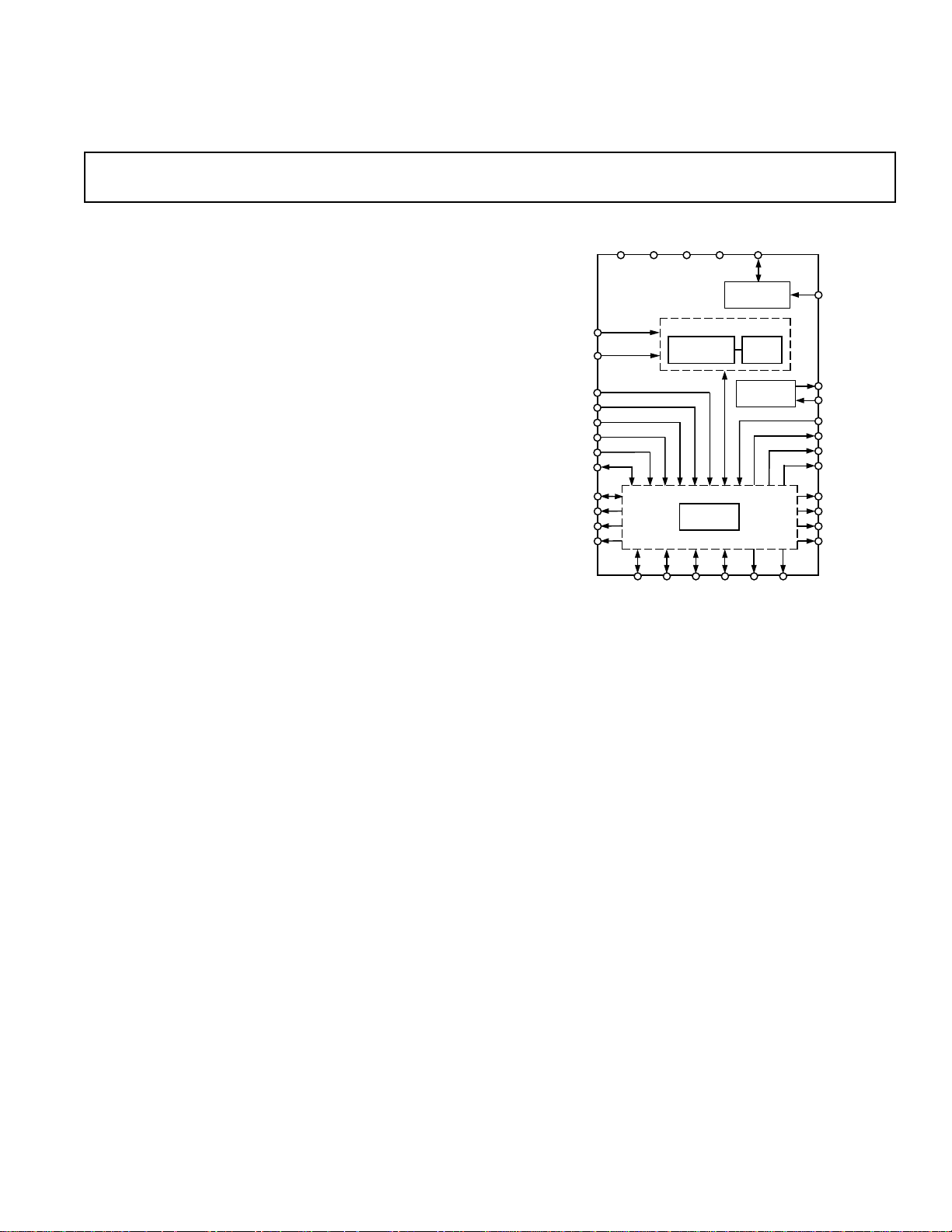
16-BIT A/D CONVERTER
Σ∆
MODULATOR
FIR
FILTER
CLOCK
CIRCUITRY
CONTROL
LOGIC
DB13
AD7722
2.5V
REFERENCE
a
FEATURES
16-Bit Sigma-Delta ADC
643 Oversampling Ratio
Up to 220 kSPS Output Word Rate
Low-Pass, Linear Phase Digital Filter
Inherently Monotonic
On-Chip 2.5 V Voltage Reference
Single Supply +5 V
High Speed Parallel or Serial Interface
GENERAL DESCRIPTION
The AD7722 is a complete low power, 16-bit, sigma-delta
ADC. The part operates from a +5 V supply and accepts a
differential input voltage range of 0 V to +2.5 V or ± 1.25 V
centered around a common-mode bias. The AD7722 provides
16-bit performance for input bandwidths up to 90.625 kHz.
The part provides data at an output word rate of 195.3 kHz.
The analog input is continuously sampled by an analog modulator eliminating the need for external sample-and-hold circuitry.
The modulator output is processed by two Finite Impulse
Response (FIR) digital filters in series. The on-chip filtering
reduces the external antialias requirements to first order, in
most cases. The group delay for the filter is 215.5 µs, while the
settling time for a step input is 431 µs. The sample rate, filter
corner frequency, and output word rate are set by an external
clock that is nominally 12.5 MHz.
Use of a single bit DAC in the modulator guarantees excellent
linearity and dc accuracy. Endpoint accuracy is ensured by onchip calibration. This calibration procedure minimizes the zeroscale and full-scale errors.
CMOS, Sigma-Delta ADC
AD7722
FUNCTIONAL BLOCK DIAGRAM
Conversion data is provided at the output register through a
flexible serial port or a parallel port. This offers 3-wire, high
speed interfacing to digital signal processors. The serial interface
operates in an internal clocking (master) mode, whereby an
internal serial data clock and framing pulse are device outputs.
Additionally, two AD7722s can be configured with the serial
data outputs connected together. Each converter alternately
transmits its conversion data on a shared serial data line.
The part provides an accurate on-chip 2.5 V reference. A
reference input/output function is provided to allow either the
internal reference or an external system reference to be used as
the reference source for the part.
The AD7722 is available in a 44-pin PQFP package and is
specified over the industrial temperature range from –40°C to
+85°C.
REV. 0
Information furnished by Analog Devices is believed to be accurate and
reliable. However, no responsibility is assumed by Analog Devices for its
use, nor for any infringements of patents or other rights of third parties
which may result from its use. No license is granted by implication or
otherwise under any patent or patent rights of Analog Devices.
One Technology Way, P.O. Box 9106, Norwood, MA 02062-9106, U.S.A.
Tel: 617/329-4700 World Wide Web Site: http://www.analog.com
Fax: 617/326-8703 © Analog Devices, Inc., 1996
Page 2

1
AD7722–SPECIFICATIONS
UNI = Logic Low or High; f
= 12.5 MHz; FS = 195.3 kSPS; REF2 = +2.5 V; TA = T
CLKLIN
(AVDD = AV
Parameter Test Conditions/Comments Min Typ Max Units
INH
2
VCM = 2.5 V, VIN(+) = VIN(–) =1.25 V pk-pk
(–) =1.25 V, VIN(+) = 0 to 2.5
or, V
3
3
IN
Input Bandwidth 0 kHz–90.625 kHz 86/84.5 90 dB
Input Bandwidth 0 kHz–100 kHz, f
Input Bandwidth 0 kHz–90.625 kHz –90/–88 dB
DYNAMIC SPECIFICATIONS
Bipolar Mode, UNI = V
Signal to (Noise + Distortion)
Total Harmonic Distortion
Input Bandwidth 0 kHz–100 kHz, f
Spurious Free Dynamic Range Input Bandwidth 0 kHz–90.625 kHz –90 dB
Input Bandwidth 0 kHz–100 kHz, f
Unipolar Mode,
UNI = V
INL
Signal to (Noise + Distortion)
Total Harmonic Distortion
3
VIN(–) = 0 V, VIN(+) = 0 to 2.5
3
Input Bandwidth 0 kHz–90.625 kHz 84.5/83 88 dB
Input Bandwidth 0 kHz–97.65 kHz –89/–87 dB
Spurious Free Dynamic Range Input Bandwidth 0 kHz–97.65 kHz –90 dB
Intermodulation Distortion –93 dB
AC CMRR V
(+) = VIN(–) = 2.5 V pk-pk
IN
= 1.25 V to 3.75 V, 20 kHz 96 dB
V
CM
Digital Filter Response
Pass-Band Ripple 0 kHz–90.625 kHz ±0.005 dB
Cutoff Frequency 96.92 kHz
Stop-Band Attenuation 104.6875 kHz to 12.395 MHz 90 dB
= +5 V 6 5%; DVDD = +5 V 6 5%; AGND = AGND1 = DGND = 0 V;
DD1
to T
MIN
; unless otherwise noted)
MAX
A Version
= 14 MHz 84.5/83 dB
CLKIN
= 14 MHz –88/–86 dB
CLKIN
= 14 MHz –88 dB
CLKIN
ANALOG INPUTS
Full-Scale Input Span V
Bipolar Mode
Unipolar Mode
Absolute Input Voltage V
(+)–VIN(–)
IN
UNI = V
UNI = V
INH
INL
(+) and VIN(–) 0 AV
IN
–V
/2 +V
REF2
0V
REF2
REF2
DD
/2 V
V
V
Input Sampling Capacitance 2pF
Input Sampling Rate Guaranteed by Design 2 × f
CLKIN
Differential Input Impedance 1/8E-09 × f
CLKIN
Hz
kΩ
CLOCK
CLKIN Mark Space Ratio 45 55 %
REFERENCE
REF1 Output Voltage 2.32 2.47 2.62 V
REF1 Output Voltage Drift 60 ppm/°C
REF1 Output Impedance 3kΩ
Reference Buffer
Offset Voltage Offset Between REF1 and REF2 ±12 mV
Using Internal Reference
REF2 Output Voltage 2.32 2.47 2.62 V
REF2 Output Voltage Drift 60 ppm/°C
Using External Reference
REF2 Input Impedance REF1 = AGND 1/16E-09 ×f
CLKIN
kΩ
External Reference Voltage Range Applied to REF1 or REF2 2.32 2.5 2.62 V
STATIC PERFORMANCE
Resolution 16 Bits
Differential Nonlinearity Guaranteed Monotonic ± 0.5 ± 1 LSB
Integral Nonlinearity ±2 LSB
After Calibration
Offset Error
Gain Error
4, 5
4
±3mV
±0.6 % FSR
Without Calibration
Offset Error ±6mV
Gain Error
5
±0.6 % FSR
Offset Error Drift ±1 LSB/°C
Gain Error Drift REF2 Is an Ideal Reference, REF1 = AGND
Unipolar Mode ±1 LSB/°C
Bipolar Mode ±0.5 LSB/°C
–2–
REV. 0
Page 3
AD7722
WARNING!
ESD SENSITIVE DEVICE
I
OL
1.6mA
I
OH
200µA
+1.6V
C
L
50pF
TO
OUTPUT
PIN
Parameter Test Conditions/Comments Min Typ Max Units
A Version
LOGIC INPUTS (Excluding CLKIN)
, Input High Voltage 2.0 V
V
INH
V
, Input Low Voltage 0.8 V
INL
CLOCK INPUT (CLKIN)
, Input High Voltage 4.0 V
V
INH
V
, Input Low Voltage 0.4 V
INL
ALL LOGIC INPUTS
, Input Current VIN = 0 V to DV
I
IN
DD
±10 µA
CIN, Input Capacitance 10 pF
LOGIC OUTPUTS
, Output High Voltage |I
V
OH
VOL, Output Low Voltage |I
| = 200 µA 4.0 V
OUT
| = 1.6 mA 0.4 V
OUT
POWER SUPPLIES
AV
DV
I
DD
DD
DD
, AV
DD1
Total from AVDD and DV
DD
4.75 5.25 V
4.75 5.25 V
75 mA
Power Consumption 375 mW
NOTES
1
Operating temperature range is as follows : A Version ; –40°C to +85°C.
2
Measurement Bandwidth = 0.5 × FS; Input Level = –0.05 dB.
3
TA = +25°C to +85°C/TA = T
4
Applies after calibration at temperature of interest.
5
Gain Error excludes reference error. The ADC gain is calibrated w.r.t. the voltage on the REF2 pin.
Specifications subject to change without notice.
MIN
to T
MAX
.
ABSOLUTE MAXIMUM RATINGS*
(TA = +25°C unless otherwise noted)
DVDD to DGND . . . . . . . . . . . . . . . . . . . . . . . . –0.3 V to 7 V
AV
AV
DD
DD
, AV
, AV
to AGND . . . . . . . . . . . . . . . . . . –0.3 V to 7 V
DD1
to DVDD . . . . . . . . . . . . . . . . . . . –1 V to +1 V
DD1
Model Temperature Package Package
AD7722AS –40°C to +85°C 44-Pin PQFP S-44
ORDERING GUIDE
AGND, AGND1 to DGND . . . . . . . . . . . . . –0.3 V to +0.3 V
Digital Inputs to DGND . . . . . . . . . . –0.3 V to DV
Digital Outputs to DGND . . . . . . . . . –0.3 V to DV
V
(+), VIN(–) to AGND . . . . . . . . . . –0.3 V to AVDD + 0.3 V
IN
REF1 to AGND . . . . . . . . . . . . . . . . –0.3 V to AV
REF2 to AGND . . . . . . . . . . . . . . . . –0.3 V to AV
+ 0.3 V
DD
+ 0.3 V
DD
+ 0.3 V
DD
+ 0.3 V
DD
DGND, AGND1, AGND2 . . . . . . . . . . . . . . . . . . . . . ±0.3 V
Operating Temperature Range . . . . . . . . . . . –40°C to +85°C
Storage Temperature Range . . . . . . . . . . . . –65°C to +150°C
Junction Temperature . . . . . . . . . . . . . . . . . . . . . . . . .+150°C
θ
Thermal Impedance . . . . . . . . . . . . . . . . . . . . . . . 95°C/W
JA
Figure 1. Load Circuit for Timing Specifications
Lead Temperature, Soldering
Vapor Phase (60 sec) . . . . . . . . . . . . . . . . . . . . . . . .+215°C
Infrared (15 sec) . . . . . . . . . . . . . . . . . . . . . . . . . . . .+220°C
*Stresses above those listed under “Absolute Maximum Ratings” may cause
permanent damage to the device. This is a stress rating only and functional
operation of the device at these or any other conditions above those indicated in the
operational section of this specification is not implied. Exposure to absolute
maximum rating conditions for extended periods may affect device reliability.
CAUTION
ESD (electrostatic discharge) sensitive device. Electrostatic charges as high as 4000 V readily
accumulate on the human body and test equipment and can discharge without detection.
Although the AD7722 features proprietary ESD protection circuitry, permanent damage may
occur on devices subjected to high energy electrostatic discharges. Therefore, proper ESD
precautions are recommended to avoid performance degradation or loss of functionality.
REV. 0
–3–
Page 4
AD7722
(AVDD= +5 V 6 5%, DVDD = +5 V 6 5%, AGND = DGND = 0 V, CL = 50 pF, TA = T
f
TIMING SPECIFICATIONS
= 12.5 MHz, SFMT = Logic Low or High, CFMT = Logic Low or High)
CLKIN
CLKIN Frequency f
CLKIN Period (t
CLK
= 1/f
)t
CLK
CLKIN Low Pulse Width t
CLKIN High Pulse Width t
CLKIN Rise Time t
CLKIN Fall Time t
FSI Low Time t
FSI Setup Time t
FSI Hold Time t
CLKIN to SCO Delay t
SCO Period
1
SCO Transition to FSO High Delay t
SCO Transition to FSO Low Delay t
SCO Transition to SDO Valid Delay t
SCO Transition from FSI
2
SDO Enable Delay Time t
SDO Disable Delay Time t
DRDY High Time t
Conversion Time
1
DRDY to CS Setup Time t
CS to RD Setup Time t
RD Pulse Width t
Data Access Time after
Bus Relinquish Time after
RD Falling Edge
RD Rising Edge t
3
CS to RD Hold Time t
RD to DRDY High Time t
SYNC/RESET Input Pulse Width t
DVAL Low Delay from SYNC/RESET t
SYNC/RESET Low Time Before CLKIN Rising t
DRDY High Delay after SYNC/RESET Low t
DRDY Low Delay after SYNC/RESET Low1t
DVAL High Delay after SYNC/RESET Low1t
CAL Setup Time t
CAL Pulse Width t
Calibration Delay from CAL High t
Unipolar Input Calibration Time, (UNI = “0”)1t
Bipolar Input Calibration Time, (UNI = “1”)1t
Conversion Results Valid, (UNI = “0”)
Conversion Results Valid, (UNI = “1”)
NOTES
1
Guaranteed by design.
2
Frame Sync is initiated on falling edge of CLKIN.
3
With RD synchronous to CLKIN t22, can be reduced up to 1 t
1
1
CLK
to T
MAX
,
MIN
Symbol Min Typ Max Units
CLK
1
2
3
4
5
6
7
8
9
t
10
11
12
13
t
14
15
16
17
t
18
19
20
21
t
22
23
24
25
26
27
28
29
30
31
34
35
36
37
37
t
38
t
38
.
0.3 12.5 15 MHz
0.067 0.08 3.33 µs
0.45 × t
0.45 × t
1
1
0.55 × t
0.55 × t
1
1
5ns
5ns
2t
CLK
20 ns
20 ns
40 ns
2t
CLK
410 ns
410 ns
38 ns
2.5 t
CLK
30 45 ns
10 30 ns
2t
64 t
CLK
CLK
0ns
0ns
t
+ 20 ns
CLK
t
+ 40 ns
CLK
t
+ 40 ns
CLK
0ns
1t
CLK
10 ns
40 ns
10 ns
50 ns
(8192 + 64) t
8192 t
CLK
CLK
10 ns
12 t
64 t
(3 × 8192 + 2 × 512) t
(4 × 8192 + 3 × 512) t
(3 × 8192 + 2 × 512 + 64) t
(4 × 8192 + 3 × 512 + 64) t
CLK
CLK
CLK
CLK
CLK
CLK
–4–
REV. 0
Page 5
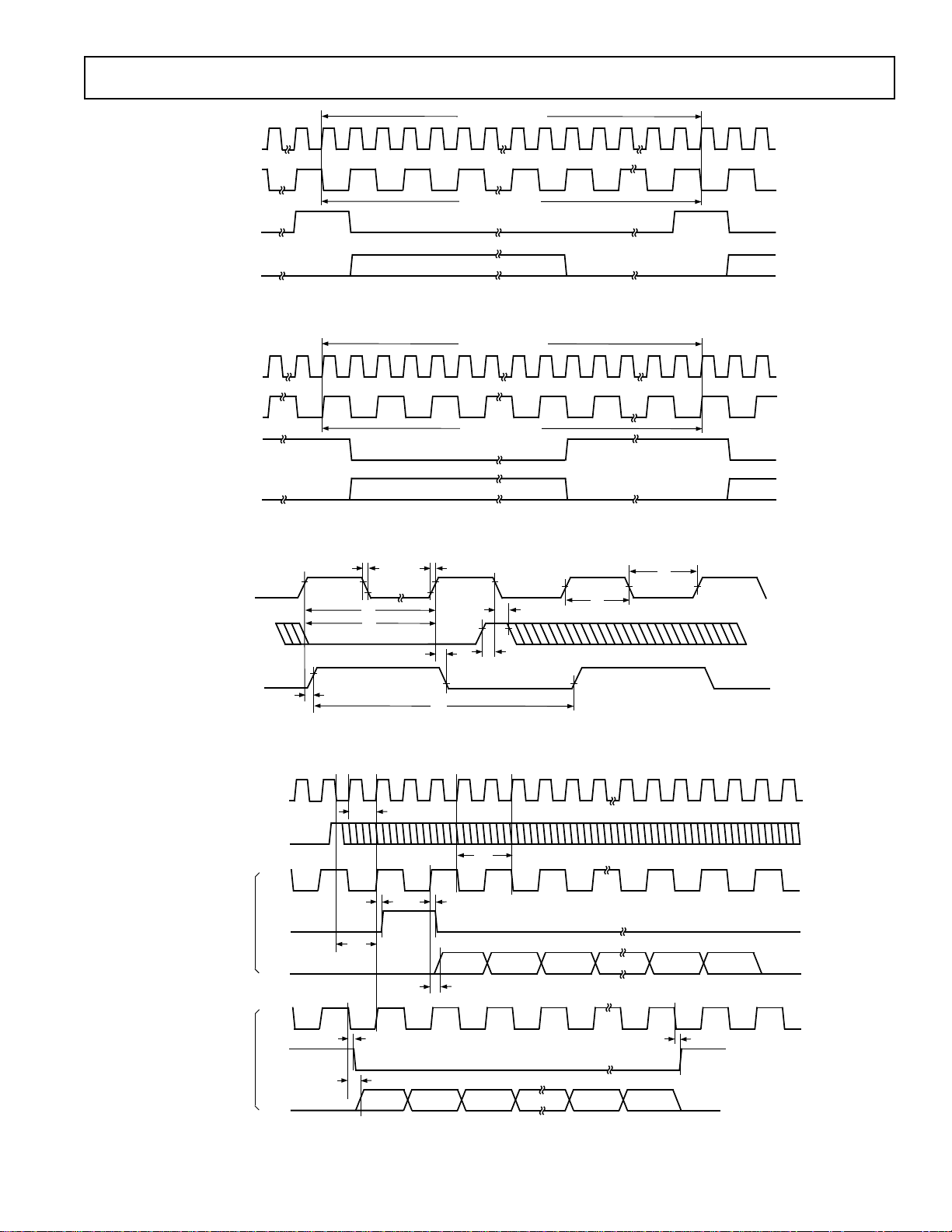
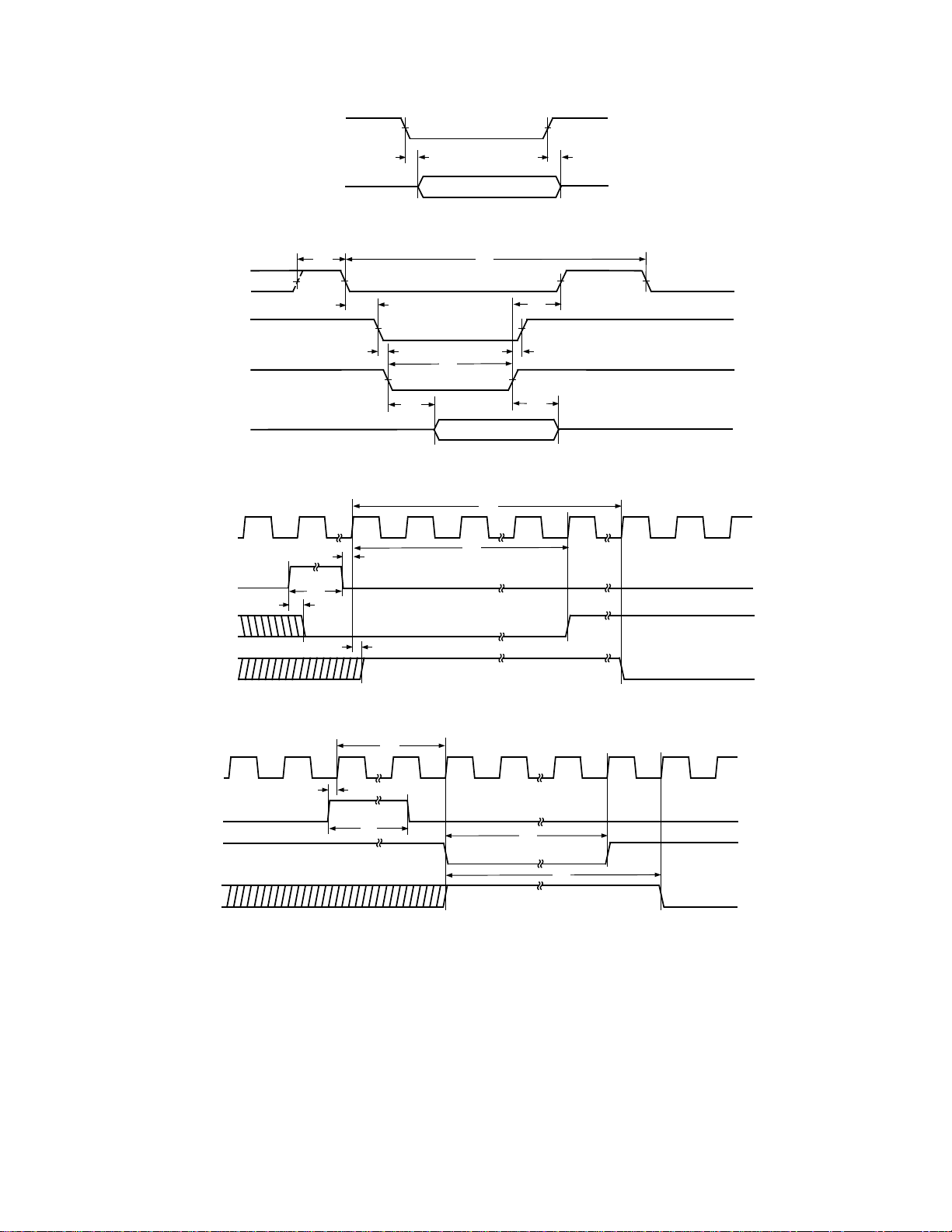
CLKIN
SCO
(CFMT = 0)
FSO
(SFMT = 0)
AD7722
64 CKLIN CYCLES
32 SCO CYCLES
SCO
ZERO FOR LAST 16 SCO CYCLESVALID DATA FOR 16 SCO CYCLES VALID
Figure 2a. Generalized Serial Mode Timing (FSI = Logic Low or High, TSI = DOE)
64 CKLIN CYCLES
CLKIN
SCO
(CFMT = 0)
FSO
(SFMT = 1)
SCO
LOW FOR 16 SCO CYCLES
VALID DATA FOR 16 SCO CYCLES
32 SCO CYCLES
HIGH FOR LAST 16 SCO CYCLES
ZERO FOR LAST 16 SCO CYCLES
Figure 2b. Generalized Serial Mode Timing (FSI = Logic Low or High, TSI = DOE)
t
4
t
t
8
t
9
t
10
t
7
3
t
2
CLKIN
FSI
SCO
2.3V
t
5
0.8V
t
1
t
6
t
9
VALID
Figure 3. Serial Mode Timing for Clock Input, Frame Sync Input and Serial Clock Output
CLKIN
t
1
FSI
t
10
SCO
SFMT = LOGIC
LOW(0)
SFMT = LOGIC
HIGH(1)
FSO
SDO
SCO
FSO
SDO
LOW FOR
D15–D0
t
11
t
14
t
12
t
13
D15 D14 D13 D1 D0
t
12
D15 D14 D13 D1 D0
t
13
t
11
Figure 4. Serial Mode Timing for Frame Sync Input, Frame Sync Output, Serial Clock Output
and Serial Data Output (CFMT = Logic Low, TSI = DOE)
REV. 0
–5–
Page 6
AD7722
DOE
t
16
SDO
t
15
Figure 5. Serial Mode Timing for Data Output Enable and Serial Data Output (TSI = Logic Low)
DRDY
t
17
t
19
t
18
t
25
DB0 – DB15
CLKIN
SYNC, RESET
DVAL
DRDY
CLKIN
CAL
DVAL
DRDY
CS
RD
t
20
t
21
t
22
VALID DATA
t
24
t
23
Figure 6. Parallel Mode Read Timing
t
30
t
t
28
t
t
27
26
t
29
31
Figure 7. SYNC and RESET Timing, Serial and Parallel Mode
t
36
t
34
t
35
t
37
t
38
Figure 8. Calibration Timing, Serial and Parallel Mode
–6–
REV. 0
Page 7
PIN FUNCTION DESCRIPTION
Mnemonic Pin No. Description
AD7722
AV
DD1
14 Clock logic power supply voltage for the analog modulator, +5 V ± 5%.
AGND1 10 Clock logic ground reference for the analog modulator.
AV
DD
20, 23 Analog Power Supply Voltage, +5 V ± 5%.
AGND 9, 13, 15, Ground reference for analog circuitry.
19, 21, 25, 26
DV
DD
39 Digital Power Supply Voltage, +5 V ± 5%.
DGND 6, 28 Ground reference for digital circuitry.
REF1 22 Reference Input/Output. REF1 connects through 3 kΩ to the output of the internal 2.5 V
reference and to the input of a buffer amplifier that drives the Σ−∆ modulator. This pin can
also be overdriven with an external reference 2.5 V.
REF2 24 Reference Input/Output. REF2 connects to the output of an internal buffer amplifier used to
to drive the Σ−∆ modulator. When REF2 is used as an input, REF1 must be connected
to AGND.
V
(+) 18 Positive terminal of the differential analog input.
IN
V
(–) 16 Negative terminal of the differential analog input.
IN
UNI 7 Analog input range select input. UNI selects the analog input range for either bipolar
or unipolar operation. A logic low input selects unipolar operation. A logic high input
selects bipolar operation.
CLKIN 11 Clock Input. Master clock signal for the device. The CLKIN pin interfaces the AD7722
internal oscillator circuit to an external crystal or to an external clock. A parallel resonant,
fundamental-frequency, microprocessor-grade crystal and a 1 MΩ resistor should be
connected between the CLKIN and XTAL pin with two capacitors connected from each
pin to ground. Alternatively, the CLKIN pin can be driven with an external CMOScompatible clock. The AD7722 is specified with a clock input frequency of 12.5 MHz.
XTAL 12 Oscillator Output. The XTAL pin connects the internal oscillator output to an external
crystal. If an external clock is used, XTAL should be left unconnected.
P/
S 8 Parallel/Serial interface select input. A logic high configures output data interface for parallel
mode operation. Serial mode operation is selected with the P/S set to a logic low.
CAL 27 Calibration Logic Input. A logic high input for a duration of one CLKIN cycle initiates a
calibration sequence for the device Gain and Offset Error.
RESET 17 Reset Logic Input. RESET is used to clear the offset and gain calibration registers. RESET is an
asynchronous input. RESET allows the user to set AD7722 to an uncalibrated state if the device
had been previously calibrated. A rising edge also resets the AD7722 Σ−∆ modulator by shorting
the integrator capacitors in the modulator. In addition RESET functions identically to the
SYNC pin described below.
CS 29 Chip select is a level sensitive logic input. CS enables the output data register for parallel mode
read operation. The CS logic level is sensed on the rising edge of CLKIN. The output data bus
is enabled when the rising edge of CLKIN senses a logic low level on CS if RD is also low. When
CS is sensed high, the output data bits DB15–DB0 will be high impedance. In serial mode tie
CS to a logic low.
SYNC 30 Synchronization Logic Input. SYNC is an asynchronous input. When using more than one
AD7722 operated from a common master clock, SYNC allows each ADC’s Σ−∆ modulator
to simultaneously sample its analog input and update its output data register. A rising edge resets
the AD7722 digital filter sequencer counter to zero. After a SYNC, conversion data is not valid
until after the digital filter settles (reference Figure 7). DVAL goes low in the serial mode. When
the rising edge of CLKIN senses a logic low on SYNC (or RESET) the reset state is released; in
parallel mode,
8192 CLKIN cycles (128 × 64/f
convolution cycle of the digital filter (64 CLKIN periods), when valid data is ready to be read
from the output data register.
DRDY goes high. After the reset state is released, DVAL returns high after
); in parallel mode, DRDY returns low after one additional
CLKIN
REV. 0
–7–
Page 8
AD7722
PIN CONFIGURATION
44-Pin PQFP (S-44)
DD
DV
SCO/DB7
FSI/DB6
40 39 3841424344 36 35 3437
AD7722
TOP VIEW
(Not to Scale)
VIN(–)
AGND
RESET
FSO/DB9
SDO/DB8
VIN(+)
AGND
DGND/DB10
DGND/DB11
DGND/DB12
DD
REF1
AV
AGND
33
DGND/DB13
32
DGND/DB14
31
DGND/DB15
30
SYNC
CS
29
28
DGND
27
CAL
26
AGND
25
AGND
24
REF2
23
AV
DD
DGND/DB2
DGND/DB1
DGND/DB0
CFMT/DRDY
DVAL/RD
DGND
UNI
P/S
AGND
AGND1
CLKIN
TSI/DB3
SFMT/DB5
DOE/DB4
1
PIN 1
IDENTIFIER
2
3
4
5
6
7
8
9
10
11
121314 15 16 17 18 192021 22
DD1
XTAL
AGND
AV
PARALLEL MODE PIN FUNCTION DESCRIPTION
Mnemonic Pin No. Description
DVAL/
RD 5 Read Input is a level sensitive logic input. The RD logic level is sensed on the rising edge of CLKIN.
This digital input can be used in conjunction with
bus is enabled when the rising edge of CLKIN senses a logic low level on
CS to read data from the device. The output data
RD if CS is also low. When
RD is sensed high, the output data bits DB15–DB0 will be high impedance.
CFMT/
DRDY 2 Data Ready Logic Output. A falling edge indicates a new output word is available to be read from out-
put data register. DRDY will return high upon completion of a read operation. If a read operation
does not occur between output updates, DRDY will pulse high for two CLKIN cycles before the next
output update. DRDY also indicates when conversion results are available after a SYNC or RESET
sequence and when completing a self-calibration.
DGND/DB15 31 Data Output Bit (MSB)
DGND/DB14 32 Data Output Bit
DGND/DB13 33 Data Output Bit
DGND/DB12 34 Data Output Bit
DGND/DB11 35 Data Output Bit
DGND/DB10 36 Data Output Bit
FSO/DB9 37 Data Output Bit
SDO/DB8 38 Data Output Bit
SCO/DB7 40 Data Output Bit
FSI/DB6 41 Data Output Bit
SFMT/DB5 42 Data Output Bit
DOE/DB4 43 Data Output Bit
TSI/DB3 44 Data Output Bit
DGND/DB2 1 Data Output Bit
DGND/DB1 2 Data Output Bit
DGND/DB0 3 Data Output Bit (LSB)
–8–
REV. 0
Page 9

AD7722
SERIAL MODE PIN FUNCTION DESCRIPTION
Mnemonic Pin No. Description
DVAL/
RD 5 Data Valid Logic Output. A logic high on DVAL indicates that the conversion result in the
output data register is an accurate digital representation of the analog voltage at the input to the
Σ−∆ modulator. The DVAL pin is set low for 8,192 CLKIN cycles if the analog input is overranged
and after initiating CAL, SYNC or RESET.
CFMT/
TSI/DB3 44 Time Slot Logic Input. The logic level on TSI sets the active state of the DOE pin. With TSI set
DOE/DB4 43 Data Output Enable Logic Input. The DOE pin controls the three-state output buffer of the SDO
SFMT/DB5 42 Serial Data Format Logic Input. The logic level on the SFMT pin selects the format of the FSO sig-
FSI/DB6 41 Frame Synchronization Logic Input. The FSI input is used to synchronize the AD7722 serial output
SCO/DB7 40 Serial Data Clock Output. The serial clock output is synchronous to the CLKIN signal and has a
SDO/DB8 38 Serial Data Output. The serial data is shifted out MSB first, synchronous with the SCO. A serial
FSO/DB9 37 Frame Sync Output. This output indicates the beginning of a word transmission on the SDO pin.
DGND/DB0 3 In serial mode these pins should be tied to DGND.
DGND/DB1 2
DGND/DB2 1
DGND/DB10 36
DGND/DB11 35
DGND/DB12 34
DGND/DB13 33
DGND/DB14 32
DGND/DB15 31
DRDY 4 Serial Clock Format Logic Input. The clock format pin selects whether the serial data, SDO, is valid
on the rising or falling edge of the serial clock, SCO. When CFMT is logic low—SDO is valid on the
falling edge of SCO if SFMT is Low; SDO is valid on the rising edge of SCO if SFMT is High.
When CFMT is logic high—SDO is valid on the rising edge of SCO if SFMT is Low; SDO is valid
on the falling edge of SCO if SFMT is High.
logic high, DOE will enable the SDO output buffer when it is a logic high, and vice versa. TSI is
used when two AD7722s are connected to the same serial data bus.
pin. The active state of DOE is determined by the logic level on the TSI pin. When the DOE logic
level equals the level on TSI pin, the serial data output, SDO, is active. Otherwise, SDO will be high
impedance. SDO can be three-state after a serial data transmission by connecting DOE to FSO.
nal. A logic low makes the FSO output a pulse one SCO cycle wide occurring every 32 SCO cycles.
With SFMT set to a logic high, the FSO signal is a frame pulse that is active low for the duration of
the 16 data bit transmission.
data register to an external source. When the falling edge of CLKIN detects a low to high transition,
the AD7722 interrupts the current data transmission, reloads the output serial shift register, resets
SCO, and transmits the conversion result. Synchronization starts immediately, and the next 127
conversions are invalid. In serial mode, DVAL remains high. FSI inputs applied synchronous to the
output data rate do not alter the serial data transmission. If FSI is tied to either a logic high or low,
the AD7722 will generate FSO outputs controlled by the logic level on SMFT.
frequency one-half the CLKIN frequency. A data transmission frame is 32 SCO cycles long.
data transmission lasts 32 SCO cycles. After the LSB is output, trailing zeros are output for the remaining 16 SCO cycles.
Depending on the logic level of the SFMT pin, the FSO signal is either a positive pulse approximately one SCO period wide or a frame pulse, which is active low for the duration of the 16 data bit
transmission (reference Figure 4).
REV. 0
–9–
Page 10

AD7722
TERMINOLOGY
Signal-to-Noise Plus Distortion Ratio (S/(N+D))
S/(N+D) is the measured signal-to-noise plus distortion ratio at
the output of the ADC. The signal is the rms magnitude of the
fundamental. Noise plus distortion is the rms sum of all of the
nonfundamental signals and harmonics to half the sampling
rate (F
/128), excluding dc. The ADC is evaluated by
CLKIN
applying a low noise, low distortion sine wave signal to the
input pins. By generating a Fast Fourier Transform (FFT)
plot, the S/(N+D) data can then be obtained from the output
spectrum.
Total Harmonic Distortion (THD)
THD is the ratio of the rms sum of the harmonics to the rms
value of the fundamental. THD is defined as:
2
2
2
2
2
+V
5
6
THD = 20 log
SQRT V
+V
+V
2
3
()
+V
4
V
1
where V1 is the rms amplitude of the fundamental and V2, V3,
V4, V5 and V6 are the rms amplitudes of the second through
sixth harmonics. The THD is also derived from the FFT plot
of the ADC output spectrum.
Spurious Free Dynamic Range (SFDR)
Defined as the difference, in dB, between the peak spurious or
harmonic component in the ADC output spectrum (up to
F
/128 and excluding dc) and the rms value of the funda-
CLKIN
mental. Normally, the value of this specification will be determined by the largest harmonic in the output spectrum of the
FFT. For input signals whose second harmonics occur in the
stop band region of the digital filter, a spur in the noise floor
limits the SFDR.
Intermodulation Distortion
With inputs consisting of sine waves at two frequencies, fa and
fb, any active device with nonlinearities will create distortion
products at sum and difference frequencies of mfa ± nfb where
m, n = 0, 1, 2, 3, etc. Intermodulation distortion terms are
those for which neither m nor n are equal to zero. For example,
the second order terms include (fa + fb) and (fa – fb), while the
third order terms include (2fa + fb), (2fa – fb), (fa + 2fb) and
(fa – 2fb).
Testing is performed using the CCIF standard where two input
frequencies near the top end of the input bandwidth are used.
In this case, the second order terms are usually distanced in
frequency from the original sine waves, while the third order
terms are usually at a frequency close to the input frequencies.
As a result, the second and third order terms are specified
separately. The calculation of the intermodulation distortion is
as per the THD specification where it is the ratio of the rms
sum of the individual distortion products to the rms amplitude
of the sum of the fundamental expressed in dB.
Pass-Band Ripple
The frequency response variation of the AD7722 in the defined
pass-band frequency range.
Pass-Band Frequency
The frequency up to which the frequency response variation is
within the pass-band ripple specification.
Cutoff Frequency
The frequency below which the AD7722’s frequency response
will not have more than 3 dB of attenuation.
Stop-Band Frequency
The frequency above which the AD7722’s frequency response
will be within its stop-band attenuation.
Stop-Band Attenuation
The AD7722’s frequency response will not have less than 90 dB
of attenuation in the stated frequency band.
Integral Nonlinearity
This is the maximum deviation of any code from a straight line
passing through the endpoints of the transfer function. The
endpoints of the transfer function are minus full scale, a point
0.5 LSB below the first code transition (100 . . . 00 to 100 . . .
01 in bipolar mode, 000 . . . 00 to 000 . . . 01 in unipolar mode)
and plus full scale, a point 0.5 LSB above the last code transition (011 . . . 10 to 011 . . . 11 in bipolar mode, 111 . . . 10 to
111 . . . 11 in unipolar mode). The error is expressed in LSBs.
Differential Nonlinearity
This is the difference between the measured and the ideal
1 LSB change between two adjacent codes in the ADC.
Common-Mode Rejection Ratio
The ability of a device to reject the effect of a voltage applied to
both input terminals simultaneously—often through variation of
a ground level—is specified as a common-mode rejection ratio.
CMRR is the ratio of gain for the differential signal to the gain
for the common-mode signal.
Unipolar Offset Error
Unipolar offset error is the deviation of the first code transition
(00 . . . 000 to 00 . . . 001) from the ideal differential voltage
(VIN(+) – VIN(–)+ 0.5 LSB) when operating in the unipolar
mode.
Bipolar Offset Error
This is the deviation of the midscale transition code (111 . . . 11
to 000 . . . 00) from the ideal differential voltage (VIN(+) –
VIN(–) – 0.5 LSB) when operating in the bipolar mode.
Gain Error
The first code transition should occur at an analog value
1/2 LSB above –full scale. The last transition should occur for
an analog value 1 1/2 LSB below the nominal full scale. Gain
error is the deviation of the actual difference between first and
last code transitions and the ideal difference between first and
last code transitions.
–10–
REV. 0
Page 11

Typical Characteristics–AD7722
INPUT FREQUENCY – kHz
dB
–85
–90
–115
0 20 100
40 60 80
–95
–100
–105
–110
SNR
SFDR
THD
CODE
DNL ERROR – LSB
1.0
0.8
–1.0
0 20000 6553540000
–0.4
–0.8
–0.6
0
–0.2
0.6
0.2
0.4
(AVDD = DVDD = 5.0 V, TA = +258C; CLKIN = 12.5 MHz, AIN = 20 kHz, Bipolar Mode; VIN(+) = 0 V to 2.5 V, VIN(–) = 1.25 V unless otherwise noted)
110
100
90
80
dB
70
60
50
–40 –30 0
SFDR
S/ (N+D)
–20 –10
INPUT LEVEL – dB
Figure 9. S/(N+D) and SFDR vs.
Analog Input Level
–85
–90
SNR
–95
THD
–100
dB
–105
SFDR
–110
–115
0 20 100
VIN (+) = VIN(–) = 1.25Vpk–pk
V
= 2.5V
CM
40 60 80
INPUT FREQUENCY – kHz
84
85
AIN = 1/5 · BW
86
87
88
dB
89
90
91
92
0 50 300
100 150 200 250
OUTPUT DATA RATE – kSPS
Figure 10. S/(N+D) vs. Output
Sample Rate
84
85
AIN = 1/5 · BW
VIN (+) = VIN(–) = 1.25Vpk–pk
86
V
= 2.5V
CM
87
88
dB
89
90
91
92
0 50 300
100 150 200 250
OUTPUT DATA RATE – kSPS
Figure 11. SNR, THD, and SFDR vs.
Input Frequency
92.0
91.5
91.0
90.5
90.0
dB
89.5
89.0
88.5
88.0
–50 0 100
TEMPERATURE – °C
50
Figure 12. SNR, THD, and SFDR vs.
Input Frequency
–94
–96
–98
–100
–102
–104
dB
–106
–108
–110
–112
–114
–116
–50 –25 100
Figure 15. THD vs. Temperature
REV. 0
THD
0255075
TEMPERATURE – °C
3RD
4TH
2ND
Figure 13. S/(N+D) vs. Output
Sample Rate
5000
4500
4000
3500
3000
2500
2000
1500
1000
FREQUENCY OF OCCURENCE
500
0
n–3 n–2 n+3
VIN(+) = VIN(–)
CLKIN = 12.5MHz
8k SAMPLES
n–1 n n+1 n+2
CODES
Figure 16. Histogram of Output
Codes with DC Input
–11–
Figure 14. SNR vs. Temperature
Figure 17. Differential Nonlinearity
Page 12

AD7722–Typical Characteristics
CLKIN FREQUENCY – MHz
POWER – mW
200
0
0 2.5 15
5 7.5 10 12.5
180
80
60
40
20
160
140
100
120
AI
DD
DI
DD
0
–154
dB
–20
–80
–100
–120
–140
–40
–60
0E+0 10E+3 20E+3 30E+3 40E+3 50E+3 60E+3 70E+3 80E+3 98E+3
AIN = 90kHz
CLKIN = 12.5 MHz
SNR = 89.6dB
S/(N+D) = 89.6dB
SFDR = –108.0dB
90E+3
(AVDD = DVDD = 5.0 V, TA = +258C; CLKIN = 12.5 MHz, AIN = 20 kHz, Bipolar Mode; VIN(+) = 0 V to 2.5 V, VIN(–) = 1.25 V unless otherwise noted)
1.0
0.8
0.6
0.4
0.2
0
–0.2
INL ERROR – LSB
–0.4
–0.6
–0.8
–1.0
0 20000 6553540000
CODE
Figure 18. Integral Nonlinearity Error
0
–20
–40
–60
–80
dB
–100
–120
–140
–154
0E+0 10E+3 20E+3 30E+3 40E+3 50E+3 60E+3 70E+3 80E+3
CLKIN = 12.5MHz
SNR = 90.1dB
S/(N+D) = 89.2dB
SFDR = –99.5dB
THD = –96.6dB
2ND = –100.9dB
3RD = –106.0dB
4TH = –99.5dB
90E+3
Figure 19. 16K Point FFT
0
–20
–40
–60
–80
dB
–100
–120
–140
–154
0E+0 10E+3 20E+3 30E+3 40E+3 50E+3 60E+3 70E+3 80E+3 96E+3
XTAL = 12.288MHz
SNR = 89.0dB
S/(N+D) = 87.8dB
SFDR = –94.3dB
THD = –93.8dB
2ND = –94.3dB
3RD = –108.5dB
4TH = –105.7dB
90E+3
98E+3
Figure 21. Power Consumption vs.
CLKIN Frequency
Figure 22. 16K Point FFT
0
AIN = 90kHz
–20
XTAL = 12.288MHz
SNR = 88.1dB
–40
S/(N+D) = 88.1dB
SFDR = –103.7dB
–60
–80
dB
–100
–120
–140
–154
0E+0 10E+3 20E+3 30E+3 40E+3 50E+3 60E+3 70E+3 80E+3 96E+3
90E+3
Figure 20. 16K Point FFT
–12–
Figure 23. 16K Point FFT
REV. 0
Page 13

AD7722
1f
CLKIN
0dB
2f
CLKIN
3f
CLKIN
OUTPUT
DATA RATE
f
CLKIN
/64
0dB
f
CLKIN
ANTIALIAS FILTER
RESPONSE
REQUIRED
ATTENUATION
CIRCUIT DESCRIPTION
The AD7722 ADC employs a sigma-delta conversion technique
that converts the analog input into a digital pulse train. The
analog input is continuously sampled by a switched capacitor
modulator at twice the rate of the clock input frequency, 2 ×
f
. The digital data that represents the analog input is in
CLKIN
the 1’s density of the bit stream at the output of the sigma-delta
modulator. The modulator outputs a bit stream at a data rate
equal to f
CLKIN
.
Due to the high oversampling rate, which spreads the quantization noise from 0 to f
/2, the noise energy contained in the
CLKIN
band of interest is reduced (Figure 24a). To reduce the quantization noise further, a high order modulator is employed to
shape the noise spectrum so that most of the noise energy is
shifted out of the band of interest (Figure 24b).
The digital filter that follows the modulator provides three main
functions. The filter performs sophisticated averaging on the
1 bit samples from the output of the modulator, while removing
the large out of band quantization noise (Figure 24c). Lastly the
digital filter reduces the data rate from f
filter to f
output data rate, F
/64 at the output of the filter. The AD7722
CLKIN
, is a little over twice the signal bandwidth,
S
at the input of the
CLKIN
which guarantees that there is no loss of data in the signal band.
Digital filtering has certain advantages over analog filtering.
First, since digital filtering occurs after the A/D conversion, it
can remove noise injected during the conversion process.
Analog filtering cannot remove noise injected during conversion. Second, the digital filter combines low pass-band ripple
with a steep roll off, while also maintaining a linear phase
response.
QUANTIZATION NOISE
f
/2
BAND OF INTEREST
a.
CLKIN
The AD7722 employs two Finite Impulse Response (FIR) filters
in series. The first filter is a 384 tap filter that samples the output
of the modulator at f
band filter that samples the output of the first filter at f
. The second filter is a 151 tap half-
CLKIN
CLKIN
/32
and decimates by 2. The implementation of this filter architecture results in a filter with a group delay of 42 conversions (84
conversions for settling to a full-scale step).
The digital filter provides 6 dB of attenuation at a frequency
(f
/128) one-half its output rate. With a clock frequency
CLKIN
of 12.5 MHz, the digital filter has a pass-band frequency of
90.625 kHz, a cutoff frequency is 96.92 kHz and stop-band
frequency of 104.6875 kHz.
Due to the sampling nature of the digital filter, the filter does
not provide any rejection at integer multiples of its input
sampling frequency. The filter response in Figure 25a shows the
unattenuated frequency bands occurring at n × f
CLKIN
where
n = 1, 2, 3. . . . At these frequencies, there are frequency bands
± f
wide (f
3 dB
either side of n × f
is the –3 dB bandwidth of the digital filter) on
3 dB
where noise passes unattenuated to the
CLKIN
output. Out of band signals coincident with any of the filter
images are aliased into the pass band. However, due to the
AD7722’s high oversampling ratio, these bands occupy only a
small fraction of the spectrum, and most broadband noise is
filtered. This means that the antialias filtering requirements in
front of the AD7722 are considerably reduced versus a conventional converter with no on-chip filtering. Figure 25b shows the
frequency response of an antialias filter. With a –3 dB corner
frequency set at f
of attenuation at f
/64, a single pole filter will provide 36 dB
CLKIN
.
CLKIN
Depending on the application, however, it may be necessary to
provide additional antialias filtering prior to the AD7722 to
eliminate unwanted signals from the frequency bands the digital
filter passes. It may also be necessary in some applications to
provide analog filtering in front of the AD7722 to ensure that
differential noise signals outside the band of interest do not
saturate the analog modulator.
REV. 0
NOISE SHAPING
BAND OF INTEREST
b.
DIGITAL FILTER CUTOFF FREQUENCY
WHICH EQUALS 97.65kHz (12.5MHz)
BAND OF INTEREST
c.
Figure 24. Sigma-Delta ADC
f
CLKIN
f
CLKIN
/2
Figure 25a. Digital Filter Frequency Response
/2
Figure 25b. Frequency Response of Antialias Filter
–13–
Page 14

AD7722
18
Φ
A
Φ
B
Φ
A
Φ
B
16
2pF
2pF
AC
GROUND
500Ω
Φ
A
Φ
B
Φ
A
Φ
B
CLKIN
VIN(+)
VIN(–)
AD7722
500Ω
APPLYING THE AD7722
Analog Input Range
The AD7722 uses differential inputs to provide common-mode
noise rejection (i.e., the converted result will correspond to the
differential voltage between the two inputs). The absolute
voltage on both inputs must lie between AGND and AV
DD
.
In the unipolar mode, the full-scale analog input range (VIN(+)
– VIN(–)) is 0 V to V
. The output code is straight binary in
REF2
the unipolar mode with 1 LSB = 38 µV. The ideal transfer
function is shown in Figure 26.
In bipolar mode, the full-scale input range is ± V
REF2
/2. The
bipolar mode allows complementary input signals. As another
example, in bipolar mode, VIN(–) can be connected to a dc bias
voltage to allow a single-ended input on VIN(+) equal to V
±V
/2. In bipolar mode the output code is 2s complement
REF2
BIAS
with 1 LSB = 38 µV. The ideal transfer function is shown in
Figure 27.
OUTPUT
CODE
111...111
111...110
111...101
111...100
000...011
000...010
000...001
000...000
–1LSB
0V
DIFFERENTIAL INPUT VOLTAGE VIN(+) – VIN(–)
V
REF2
Figure 26. Unipolar Mode Transfer Function
OUTPUT
CODE
011...111
011...110
000...010
000...001
000...000
111...111
111...110
100...001
100...000
–V
REF2
+V
/2–1LSB
REF2
DIFFERENTIAL INPUT VOLTAGE VIN(+) – VIN(–)
0V
Figure 27. Bipolar Mode Transfer Function
Differential Inputs
The analog input to the modulator is a switched capacitor
design. The analog signal is converted into charge by highly
linear sampling capacitors. A simplified equivalent circuit
diagram of the analog input is shown in Figure 28. A signal
source driving the analog input must be able to provide the
charge onto the sampling capacitors every half CLKIN cycle
and settle to the required accuracy within the next half cycle.
Figure 28. Analog Input Equivalent Circuit
Since the AD7722 samples the differential voltage across its
analog inputs, low noise performance is attained with an input
circuit that provides low common-mode noise at each input.
The amplifiers used to drive the analog inputs play a critical role
in attaining the high performance available from the AD7722.
When a capacitive load is switched onto the output of an op
amp, the amplitude will momentarily drop. The op amp will try
to correct the situation and in the process hits its slew rate limit.
This nonlinear response, which can cause excessive ringing, can
lead to distortion. To remedy the situation, a low-pass RC filter
can be connected between the amplifier and the input to the
AD7722 as shown in Figure 29. The external capacitor at each
input aids in supplying the current spikes created during the
sampling process. The resistor in this diagram, as well as
creating the pole for the antialiasing, isolates the op amp from
the transient nature of the load.
ANALOG
INPUT
R
C
R
C
VIN(+)
AD7722
VIN(–)
Figure 29. Simple RC Antialiasing Circuit
The differential input impedance of the AD7722 switched
capacitor input varies as a function of the CLKIN frequency,
given by the equation:
9
8 × f
10
CLKIN
kΩ
ZIN=
–14–
REV. 0
Page 15

AD7722
24
3kΩ
AD7722
REFERENCE
BUFFER
22
1V
2.5V
REFERENCE
SWITCHED-CAP
DAC REF
REF1
REF2
COMPARATOR
100nF
AD780
1
2
3
4
8
7
6
5
NC
+V
IN
TEMP
GND
O/P
SELECT
NC
V
OUT
TRIM
22nF
1µF
24
REF2
AD7722
22µF
100nF
22
REF1
+5V
Even though the voltage on the input sampling capacitors may
not have enough time to settle to the accuracy indicated by the
resolution of the AD7722, as long as the sampling capacitor
charging follows the exponential curve of RC circuits, only the
gain accuracy suffers if the input capacitor is switched away
too early.
An alternative circuit configuration for driving the differential
inputs to the AD7722 is shown in Figure 30.
R
100Ω
R
100Ω
C
2.7nF
C
2.7nF
C
2.7nF
VIN(+)
AD7722
VIN(–)
Figure 30. Differential Input with Antialiasing
A capacitor between the two input pins sources or sinks charge
to allow most of the charge that is needed by one input to be
effectively supplied by the other input. This minimizes undesirable charge transfer from the analog inputs to and from ground.
The series resistor isolates the operational amplifier from the
current spikes created during the sampling process and provides
a pole for antialiasing. The –3 dB cutoff frequency
(f
) of the antialias filter is given by Equation 1, and the
3 dB
attenuation of the filter is given by Equation 2.
=
6 π RC
1
(1)
2
f
f
(2)
3dB
f
3dB
Attenuation = 20 log 1/ 1+
The choice of the filter cutoff frequency will depend on the
amount of roll-off that is acceptable in the pass band of the
digital filter and the required attenuation at the first image
frequency. For example, when operating the AD7722 with a
12.5 MHz clock; with the typical values of R and C of 100 Ω and
2.7 nF shown in Figure 30, the –3 dB cutoff frequency (f
3 dB
creates less than 1 dB of in band (90.625 kHz) roll-off and
provides about 36 dB attenuation at the first image frequency.
The capacitors used for the input antialiasing circuit must have
low dielectric absorption to avoid distortion. Film capacitors
such as Polypropylene, Polystyrene or Polycarbonate are
suitable. If ceramic capacitors are used, they must have NP0
dielectric.
Applying the Reference
The reference circuitry used in the AD7722 includes an on-chip
2.5 V band gap reference and a reference buffer circuit. The
block diagram of the reference circuit is shown in Figure 31.
The internal reference voltage is connected to REF1 through a
3kΩ resistor and is internally buffered to drive the analog
modulator’s switched cap DAC (REF2). When using the
REV. 0
internal reference, connect 100 nF between REF1 and AGND.
If the internal reference is required to bias external circuits, use
an external precision op amp to buffer REF1.
Figure 31. Reference Circuit Block Diagram
The AD7722 can operate with its internal reference or an
external reference can be applied in two ways. An external
reference can be connected to REF1, overdriving the internal
reference. However, there will be an error introduced due to
the offset of the internal buffer amplifier. For lowest system
gain errors when using an external reference, REF1 is grounded
(disabling the internal buffer) and the external reference is
connected to REF2.
In all cases, since the REF2 voltage connects to the analog
modulator, a 100 nF capacitor must connect directly from
REF2 to AGND. The external capacitor provides the charge
required for the dynamic load presented at the REF2 pin
(Figure 32).
Φ
A
REF2
24
100nF
)
CLKIN
4pF
4pF
Φ
B
Φ
Φ
Φ
A
A
B
AD7722
Φ
B
Φ
A
SWITCHED-CAP
DAC REF
Φ
B
Figure 32. REF2 Equivalent Input Circuit
The AD780 is ideal to use as an external reference with the
AD7722. Figure 33 shows a suggested connection diagram.
Figure 33. External Reference Circuit Connection
–15–
Page 16

AD7722
1MΩ
XTAL CLKIN
AD7722
Input Circuits
Figures 34 and 35 show two simple circuits for bipolar mode
operation. Both circuits accept a single-ended bipolar signal
source and create the necessary differential signals at the input
to the ADC.
The circuit in Figure 34 creates a 0 V to 2.5 V signal at the
VIN(+) pin to form a differential signal around an initial bias of
1.25 V. For single-ended applications best THD performance is
obtained with VIN(–) set to 1.25 V rather than 2.5 V. The input
to the AD7722 can also be driven differentially with a complementary input as shown in Figure 35.
In this case, the input common-mode voltage is set to 2.5 V.
The 2.5 V p-p full-scale differential input is obtained with a
1.25 V p-p signal at each input in antiphase. This configuration
minimizes the required output swing from the amplifier circuit
and is useful for single supply applications.
12pF
AIN =
±1.25V
1kΩ 1kΩ
1/2
OP275
1kΩ
1kΩ
1kΩ
12pF
1/2
OP275
374kΩ
374kΩ
1nF
1nF
100nF
100nF
10nF
18
VIN(+)
16
VIN(–)
DIFFERENTIAL
INPUT = 2.5V p-p
VIN(–) BIAS
VOLTAGE = 1.25V
22
REF1
AD7722
24
REF2
The 1 nF capacitors at each ADC input store charge to aid the
amplifier settling as the input is continuously sampled. A
resistor in series with the drive amplifier output and the 1 nF
input capacitor may also be used to create an antialias filter.
Clock Generation
The AD7722 contains an oscillator circuit to allow a crystal or
an external clock signal to generate the master clock for the
ADC. The connection diagram for use with crystal is shown in
Figure 36, below. Consult the crystal manufacturer’s recommendation for the load capacitors.
Figure 36. Crystal Oscillator Connection
An external clock must be free of ringing and have a minimum
rise time of 5 ns. Degradation in performance can result, as high
edge rates increase coupling that can generate noise in the
sampling process. The connection diagram for an external clock
source (Figure 37) shows a series damping resistor connected
between the clock output and the clock input to the AD7722.
The optimum resistor will depend on the board layout and the
impedance of the trace connecting to the clock input.
CLOCK
CIRCUITRY
25–150Ω
AD7722
CLKIN
Figure 34. Single-Ended Analog Input Circuit for Bipolar
Mode Operation
12pF
AIN =
±0.625V
1kΩ
1/2
OP275
R
R
1kΩ
1kΩ
12pF
1/2
OP275
OP07
1kΩ
1nF
1nF
100nF
100nF
16
VIN(–)
DIFFERENTIAL
INPUT = 2.5V p-p
COMMON MODE
VOLTAGE = 2.5V
18
VIN(+)
AD7722
22
REF1
24
REF2
Figure 35. Single-Ended to Differential Analog Input
Circuit for Bipolar Mode Operation
Figure 37. External Clock Oscillator Connection
A low phase-noise clock should be used to generate the ADC
sampling clock because sampling clock jitter effectively modulates the input signal and raises the noise floor. The sampling
clock generator should be isolated from noisy digital circuits,
grounded and heavily decoupled to the analog ground plane.
The sampling clock generator should be referenced to the
analog ground plane in a split-ground system. However, this is
not always possible because of system constraints. In many
cases, the sampling clock must be derived from a higher
frequency multipurpose system clock that is generated on the
digital ground plane. If the clock signal is passed between its
origin on a digital ground plane to the AD7722 on the analog
ground plane, the ground noise between the two planes adds
directly to the clock and will produce excess jitter. The jitter can
cause degradation in the signal-to-noise ratio and also produce
unwanted harmonics.
This can be remedied somewhat by transmitting the sampling
clock signal as a differential one, using either a small RF transformer or a high speed differential driver and receiver such as
PECL. In either case, the original master system clock should be
generated from a low phase noise crystal oscillator.
–16–
REV. 0
Page 17

AD7722
Varying the Master Clock
Although the AD7722 is specified with a master clock of
12.5 MHz, the AD7722 operates with clock frequencies up to
15 MHz and as low as 300 kHz. The input sample rate, output
word rate, and the frequency response of the digital filter are
directly proportional to the master clock frequency. For example,
reducing the clock frequency to 5 MHz leads to an analog input
sample rate of 10 MHz, an output word rate of 78.125 kSPS, a
pass-band frequency of 36.25 kHz, a cutoff frequency of
38.77 kHz, and a stop band frequency of 41.875 kHz.
SYSTEM SYNCHRONIZATION AND CONTROL
The AD7722 digital filter contains a sequencer block that
controls the digital interface and all the control logic needed to
operate the digital filter. A 14-bit cycle counter keeps track of
where the filters are in their overall operating cycle and decodes
the digital interface signals to the AD7722. The cycle counter
has a number of important transition points. In particular, the
bottom six bits control the convolution counter that decimates
by 64 to the update rate of the output data register. The counter’s
top bit is used to provide ample time (8192 CLKIN cycles) to
allow the modulator and digital filter to settle as the AD7722
sequences through its autocalibration process. The counter
increments on the rising edge of the signal at the CLKIN pin and
all of the digital I/O signals are synchronous with this clock. The
upper bit of this counter also controls when DVAL or DRDY
indicates valid data is available in the output data register after a
SYNC, RESET, CAL or an initial FSI. During normal operation the delay of 128 conversion (8192 CLKIN cycles) should
not be confused with actual settling time (5376 CLKIN cycles)
and group delay (2688 CLKIN cycles) of the of the digital filter.
SYNC Input
The SYNC input provides a synchronization function for use in
parallel or serial mode. SYNC allows the user to start gathering
samples of the analog input from a known point in time. This
allows a system using multiple AD7722s, operated from a
common master clock, to be synchronized so that each ADC
updates its output register simultaneously. The SYNC input
resets the digital filter without affecting the contents of the
calibration registers.
In a system using multiple AD7722s, a common signal to their
sync input will synchronize their operation. On the rising edge
of SYNC, the digital filter sequencer counter is reset to zero.
The filter is held in a reset state until a rising edge on CLKIN
senses SYNC low. A SYNC pulse, one CLKIN cycle long, can
be applied synchronous to the falling edge of CLKIN. This way,
on the next rising edge of CLKIN, SYNC is sensed low, the
filter is taken out of its reset state and multiple parts start to
gather input samples.
In serial mode DVAL remains low for 8192 CLKIN cycles to
allow the modulator and digital filter to settle. In parallel mode
DRDY remains high for an additional 64 CLKIN cycles when
valid data is loaded into the output register. After a SYNC,
conversion data is not valid until the digital filter settles (reference Figure 7).
DVAL
The DVAL pin, when used in the serial mode, indicates if
invalid data may be present at the ADC output. There are four
events which can cause DVAL to be deasserted and they have
different implications for how long the results should be
considered invalid.
DVAL is set low if there is an overflow condition in the first
stage of the digital filter. The overflow can result from an analog
input signal nearly twice the allowable maximum input span.
When an overflow condition is detected, DVAL is set low for
64 CLKIN cycles, (one output period) and the output data is
clipped to either positive or negative full scale depending on the
sign of the overflow. After the next convolution is completed
(64 CLKIN cycles), if the overflow condition does not exist,
DVAL goes high to indicate a valid output is available. Otherwise DVAL will remain low until the overflow condition is
eliminated.
The second stage digital filter can overflow as a result of
overflow from the first stage. The overflow condition is detected
when the second stage filter calculates a conversion result that
exceeds either plus or minus full scale (i.e., below –32,768 or
above 32,767 in bipolar mode). When the overflow is detected,
DVAL is set low, and the output register is updated with either
positive or negative full scale, depending on the sign of the
overload. After the next convolution is completed, DVAL
returns high if the next conversion result is within the full-scale
range.
As with all high order sigma-delta modulators, large overloads
on the analog input can cause the modulator to go unstable.
The modulator is designed to be stable with input signals as
high as twice full scale within the input bandwidth. Out of band
signals as high as the full-scale range will not cause instability.
When instability is detected by internal circuits, DVAL is set
low, and the output is clipped to either positive or negative full
scale depending on the polarity of the overload. The modulator
is reset to a stable state, and the digital filter sequencer counter
is reset. DVAL is set low for a minimum of 8192 CLKIN cycles
while the modulator settles out, and the digital filter accumulates new samples. DVAL returns high to indicate valid data is
available from the serial output register 8192 CLKIN cycles
after the overload condition is removed.
Lastly, DVAL also indicates when valid data is available at the
serial interface after initial power-up or upon completion of a
CAL, RESET or SYNC sequence.
Reset Input
The AD7722 RESET input controls the digital filter the same
as the SYNC input described above. Additionally, it resets the
modulator by shorting its integrator capacitors and clears the
on-chip calibration registers so that the conversion results are
not corrected for offset or gain error.
Power-On Reset
A power-on reset function is provided to reset the AD7722
internal logic after initial power-up. On power-up the offset and
gain calibration registers are cleared.
REV. 0
–17–
Page 18

AD7722
AD7722
ADDR
DECODE
DB0–15
DRDY
CS
RD
16 16
74XX16374
OR
74XX16244
OE
D0–15
RD
INTERRUPT
ADDR
DSP/µC
Offset and Gain Calibration
A calibration of offset and gain errors can be performed in both
serial and parallel modes by initiating a calibration cycle. During
this cycle, offset and gain registers in the filter are loaded with
values representing the dc offset of the analog modulator and a
modulator gain correction factor. The correction factors are
determined by an on-chip microcontroller measuring the
conversion results for three different input conditions: minus
full scale (–FS), plus full scale (+FS), and midscale. In normal
operation, the offset register is subtracted from the digital filter
output, and this result is then multiplied by the gain correction
factor to obtain an offset and gain corrected final result.
The calibration cycle is controlled by internal logic, and the user
need only initiate the cycle. A calibration is initiated when the
rising edge of CLKIN senses a high level on the CAL input.
There is an uncertainty of up to 64 CLKIN cycles before the
calibration cycle actually begins because the current conversion
must complete before calibration commences. The calibration
values loaded into the registers only apply for the particular
analog input mode (bipolar/unipolar) selected when initiating
the calibration cycle. On changing to a different analog input
mode, a new calibration must be performed.
During the calibration cycle, in unipolar mode, the offset of the
analog modulator is evaluated; the differential inputs to the
modulator are shorted internally to AGND. Once calibration
begins, DVAL goes low and
DRDY goes high indicating there is
invalid data in the output register. After 8192 CLKIN cycles,
when the modulator and digital filter settle, the average of eight
output results (512 CLKIN cycles) is calculated and stored in
the offset register. In unipolar mode, this result also represents
minus full scale, required to calculate the gain correction factor.
The gain correction factor can then be determined by internally
switching the inputs to +FS (V
). The positive input of the
REF2
modulator is switched to the reference voltage and the negative
input to AGND. Again, when the modulator and digital filter
settle, the average of the eight output results is used to calculate
the gain correction factor.
In bipolar mode, an additional measurement is required since
zero scale is not the same as –FS. Therefore, calibration in
bipolar mode requires an additional 8704 CLKIN cycles. Zero
scale is similarly determined by shorting both analog inputs to
AGND. Then the inputs are internally reconfigured to apply
+FS and –FS (+V
/2 and –V
REF2
/2) to determine the gain
REF2
correction factor.
After the calibration registers have been loaded with new values,
the inputs of the modulator are switched back to the input pins.
However, correct data is available at the interface only after the
modulator and filter have settled to the new input values.
Should the part see a rising edge on the SYNC or RESET pin
during a calibration cycle, the calibration cycle is discontinued,
and a synchronization operation or reset will be performed.
The calibration registers are static. They need to be updated
only if unacceptable drifts in analog offsets or gain are expected.
After power-up, a RESET is not mandatory since power-on
reset circuitry clears the offset and gain registers. Care must be
taken to ensure the CAL pin is held low during power-up.
Before initiating a calibration routine, ensure the supplies and
reference input have settled, and that the voltage on the analog
input pins is between the supply voltages.
DATA INTERFACING
The AD7722 offers a choice of serial or parallel data interface
options to meet the requirements of a variety of system configurations. In parallel mode, multiple AD7722s can be easily
configured to share a common data bus. Serial mode is ideal
when it is required to minimize the number of data interface
lines connected to a host processor. In either case, careful
attention to the system configuration is required to realize the
high dynamic range available with the AD7722. Consult the
recommendations in the “Power Supply Grounding and
Layout” section. The following recommendations for parallel
interfacing also apply for the system design in serial mode.
Parallel Interface
When using the AD7722, place a buffer/latch adjacent to the
converter to isolate the converter’s data lines from any noise
which may be on the data bus. Even though the AD7722 has
three-state outputs, use of an isolation latch represents good
design practice. This arrangement will inject a small amount of
digital noise on the AD7722 ground plane; these currents
should be quite small and can be minimized by ensuring that
the converter input/output does not drive a large fanout (they
normally can’t by design). Minimizing the fanout on the
AD7722’s digital port will also keep the converter logic transitions relatively free from ringing and thereby minimize any
potential coupling into the analog port of the converter.
The simplified diagram (Figure 38) shows how the parallel
interface of the AD7722 can be configured to interface with the
system data bus of a microprocessor or a modern microcontroller such as the MC68HC16 or 8XC251.
Figure 38. Parallel Interface Connection
With CS and RD tied permanently low the data output bits are
always active. When the
CLKIN cycles, the rising edge of
DRDY output goes high for two
DRDY is used to latch the
conversion data before a new conversion result is loaded into the
output data register. The falling edge of
DRDY then sends an
appropriate interrupt signal for interface control. Alternatively
if buffers are used instead of latches the falling edge of
DRDY
provides the necessary interrupt when a new output word is
available from the AD7722.
–18–
REV. 0
Page 19

AD7722
CFMT SDO
SFMT SCO
TSI
FSO
FSI DOE
CLKIN
AD7722
MASTER
FSI DOE
CLKIN SDO
CFMT
SCO
SFMT FSO
TSI
AD7722
SLAVE
DV
DD
DV
DD
DGND
FROM
CONTROL
LOGIC
TO HOST
PROCESSOR
SERIAL INTERFACE
The AD7722’s serial data interface port allows easy interfacing
to industry standard digital signal processors. The AD7722
operates solely in the master mode providing three serial data
output pins for transfer of the conversion results. The serial data
clock output (SCO), serial data output (SDO) and frame sync
output (FSO) are all synchronous with CLKIN. SCO frequency
is always one-half the CLKIN frequency. FSO is continuously
output at the conversion rate of the ADC (FCLKIN/64). The
generalized timing diagrams in Figure 2 show how the AD7722
may be used to transmit its conversion results.
Serial data shifts out of the SDO pin synchronous with SCO.
The FSO is used to frame the output data transmission to an
external device. An output data transmission is 32 SCO cycles
in duration. The serial data shifts out of the SDO pin MSB first,
LSB last for a duration of 16 SCO cycles. For the next 16 SCO
cycles SDO outputs zeros.
Two control inputs, SFMT and CFMT, select the format for
the serial data transmission. FSO is either a pulse (approximately one SCO cycle in duration) or a square wave with a
period of 32 SCO cycles, depending on the state of the SFMT.
The logic level applied to SFMT also determines if the serial
data is valid on the rising or falling edge of the SCO. The clock
format pin, CFMT, simply switches the phase of SCO for the
selected FSO format.
With a logic low level on SFMT and CFMT set low (Figure 4),
FSO pulses high for one SCO cycle at the beginning of a data
transmission frame. When FSO goes low, the MSB is available
on the SDO pin after the rising edge of SCO and can be latched
on the SCO falling edge.
With a logic high level on SFMT and CFMT set low (Figure 4),
the data on the SDO pin is available after the falling edge of
SCO and can be latched on the SCO rising edge. FSO goes low
at the beginning of a data transmission frame when the MSB is
available and returns high after 16 SCO cycles.
The Frame Sync Input (FSI) can be used if the AD7722
conversion process must be synchronized to an external source.
FSI is an optional signal; if FSI is grounded or tied high frame,
syncs are internally generated. Frame sync allows the conversion data presented to the serial interface to be a filtered and
decimated result derived from a known point in time. FSI can
be applied once after power-up, or it can be a periodic signal,
synchronous to CLKIN, occurring every 64 CLKIN cycles.
When FSI is applied for the first time, or if a low to high transition
is detected that is not synchronized to the output word rate, the
next 127 conversions should be considered invalid while the
digital filter accumulates new samples. Figure 4 shows how the
frame sync signal resets the serial output interface and how the
AD7722 will begin to output its serial data transmission frame.
A common frame sync signal can be applied to two or more
AD7722s to synchronize them to a common master clock.
Two Channel Multiplexed Operation
Three additional serial interface control pins (DOE, TSI and
CFMT) are provided. The connection diagram in Figure 39
shows how they are used to allow the serial data outputs of two
AD7722s to easily share one serial data line. Since a serial data
transmission frame lasts 32 SCO cycles, two AD7722s can share
a single data line by alternating transmission of their 16-bit
output data onto one SDO pin.
Figure 39. Connection for Two Channel Multiplexed
Operation
The Data Output Enable pin (DOE) controls SDO’s output
buffer. When the logic level on DOE matches the state of the
TSI pin, the SDO output buffer drives the serial dataline;
otherwise the output of the buffer goes high impedance. The
serial format pin (SFMT) is set high to chose the frame sync
output format. The clock format pin (CFMT) is set high so that
CLKIN
t
1
FSI
REV. 0
DOE (MASTER & SLAVE)
SCO
FSO (MASTER)
FSI (SLAVE)
SDO (MASTER)
SDO (SLAVE)
D1 D0
Figure 40. Timing for Two Channel Multiplexed Operation
t
14
t
12
t
15
D14 D1 D0
D15
t
16
t
11
t
16
t
15
D15 D14
–19–
Page 20

AD7722
serial data is made available on SDO after the rising edge of
SCO and can be latched on the SCO falling edge.
The master device is selected by setting TSI to a logic low and
connecting its FSO to DOE. The slave device is selected with its
TSI pin tied high, and both its FSI and DOE are controlled
from the master’s FSO. Since the FSO of the master controls
the DOE input of both the master and slave, one ADCs SDO is
active while the other is high impedance (Figure 40). When the
master transmits its conversion result during the first 16 SCO
cycles of a data transmission frame, the low level on DOE sets
the slave’s SDO high impedance. Once the master completes
transmitting its conversion data, its FSO goes high and triggers
the slave’s FSI to begin its data transmission frame.
Serial Interfacing to DSPs
In serial mode, the AD7722 can be interfaced directly to several
industry standard DSPs. In all cases, the AD7722 operates as
the master with the DSP operating as the slave. The AD7722
outputs its own serial clock (SCO) to transmit the digital word
on the SDO pin to a DSP. The DSP’s serial interface is synchronized to the data transmission provided by the FSO signal.
Since the serial data clock from the AD7722 is always one-half
the CLKIN frequency, DSPs that can accept relatively high
serial clock frequencies are required. The ADSP-21xx family of
DSPs can operate with a maximum serial clock of 13.824 MHz;
the DSP56002 allows a maximum serial clock of 13.3 MHz;
while the TMS320C5x-57 accepts a maximum serial clock of
10.989 MHz. To interface the AD7722 to other DSPs, the
master clock frequency of the AD7722 can be reduced so that
the SCO frequency equals the maximum allowable frequency of
the serial clock input to the DSP. When the AD7722 is operated
with a lower CLKIN frequency (< 10 MHz), DSPs such as the
TMS320C20/C25 and DSP56000/1 can be used.
Figures 41 to 43 show the interfaces between the AD7722 and
several DSPs. In all cases, the interface control pins, TSI, DOE,
SFMT, CFMT, SYNC, and FSI can be permanently hardwired
together to either DGND or DVDD. Alternatively, SFMT or
CFMT can be tied either high or low to configure the serial data
interface for the particular format required by the DSP. The
frame synchronization signal, FSI, can be applied from the user’s
system control logic.
FSO
AD7722
SDO
SCO
Figure 41. AD7722 to ADSP-21xx Interface
RFS
ADSP-21xx
DR
SCLK
FSO
AD7722
SDO
SCO
SC1
DSP56001/2/3
SRD
SCK
Figure 42. AD7722 to DSP56000 Interface
FSO
AD7722
SDO
SCO
FSR
TMS320CXX
DR
CLKR
Figure 43. AD7722 to TMS320C20/25/50 Interface
Grounding and Layout
The analog and digital power supplies to the AD7722 are
independent and separately pinned out to minimize coupling
between analog and digital sections within the device. The
AD7722 should be treated as an analog component and
grounded and decoupled to the analog ground plane. All the
AD7722 ground pins should be soldered directly to a ground
plane to minimize series inductance. All converter power pins
should be decoupled to the analog ground plane. To achieve the
best decoupling, place surface mount capacitors as close as
possible to the device, ideally right up against the device pins.
The printed circuit board that houses the AD7722 should use
separate ground planes for the analog and the digital interface
circuitry. All converter power pins should be decoupled to the
analog ground plane, and all interface logic circuit power pins
should be decoupled to the digital ground plane. This facilitates
the use of ground planes, which can physically separate sensitive
analog components from the noisy digital system. Digital and
analog ground planes should only be joined in one place and
should not overlap to minimize capacitive coupling between
them.
Separate power supplies for AVDD and DVDD are also highly
desirable. The digital supply pin DVDD should be powered
from a separate analog supply, but if necessary DVDD may
share its power connection to AVDD. Refer to the connection
diagram (Figure 44). The 10 Ω resistor, in series with the
DVDD pin, is required to dampen the effects of the fast
switching currents into the digital section of the AD7722. The
ferrite is also recommended to filter high frequency signals from
corrupting the analog power supply.
–20–
REV. 0
Page 21

AD7722
AVDD1
AGND1
AV
DD
AGND
AV
DD
AGND
DV
DD
DGND
DGND
14
10
20
19
23
25
39
6
28
100nF
100nF
100nF
1nF
10Ω
100µF10µF100µF
100nF10µF
+5V
A minimum etch technique is generally best for ground planes
because it gives the best shielding. Noise can be minimized by
paying attention to the system layout and preventing different
signals from interfering with each other. High level analog
signals should be separated from low level analog signals, and
both should be kept away from digital signals. In waveform
sampling and reconstruction systems, the sampling clock
(CLKIN) is as vulnerable to noise as any analog signal. CLKIN
should be isolated from the analog and digital systems. Fast
switching signals like clocks should be shielded with their
associated ground to avoid radiating noise to other sections of
the board, and clock signals should never be routed near the
analog inputs.
Avoid running digital lines under the device as these will couple
noise onto the die. The analog ground plane should be allowed
to run under the AD7722 to shield it from noise coupling. The
power supply lines to the AD7722 should use as large a trace as
possible (preferably a plane) to provide a low impedance path
and reduce the effects of glitches on the power supply line.
Avoid crossover of digital and analog signals. Traces on opposite
OUTLINE DIMENSIONS
Dimensions shown in inches and (mm).
sides of the board should run at right angles to each other. This
will reduce the effects of feedthrough through the board.
Figure 44. Power Supply Decoupling
44-Pin PQFP
(S-44)
0.557 (14.15)
34
44
33
1
0.033 (0.84)
0.029 (0.74)
0.537 (13.65)
0.398 (10.10)
0.390 (9.90)
TOP VIEW
(PINS DOWN)
23
22
12
11
0.018 (0.45)
0.012 (0.30)
0.096 (2.44)
PLANE
MAX
0.083 (2.11)
0.077 (1.96)
8°
0°
0.040 (1.02)
0.032 (0.81)
0.037 (0.95)
0.026 (0.65)
SEATING
0.040 (1.02)
0.032 (0.81)
REV. 0
–21–
Page 22

–22–
Page 23

–23–
Page 24

C2208–12–10/96
–24–
–24–
PRINTED IN U.S.A.
 Loading...