

Page 1
CMOS 16-Bit,
a
FEATURES
16-Bit Sigma-Delta ADC
468.75 kHz Output Word Rate (OWR)
No Missing Codes
Low-Pass Digital Filter
High Speed Serial Interface
Linear Phase
229.2 kHz Input Bandwidth
Power Supplies: AV
Standby Mode (70 mW)
Parallel Mode (12-Bit/312.5 kHz OWR)
GENERAL DESCRIPTION
The AD7721 is a complete low power, 12-/16-bit, sigma-delta
ADC. The part operates from a +5 V supply and accepts a
differential input of 0 V to 2.5 V or ± 1.25 V. The analog input
is continuously sampled by an analog modulator at twice the
clock frequency eliminating the need for external sample-andhold circuitry. The modulator output is processed by two finite
impulse response (FIR) digital filters in series. The on-chip
filtering reduces the external antialias requirements to first order
in most cases. Settling time for a step input is 97.07 µs while
the group delay for the filter is 48.53 µs when the master clock
equals 15 MHz.
The AD7721 can be operated with input bandwidths up to
229.2 kHz. The corresponding output word rate is 468.75 kHz.
The part can be operated with lower clock frequencies also.
The sample rate, filter corner frequency and output word rate
will be reduced also, as these are proportional to the external
clock frequency. The maximum clock frequencies in parallel
mode and serial mode are 10 MHz and 15 MHz respectively.
, DVDD: +5 V 6 5%
DD
468.75 kHz, Sigma-Delta ADC
AD7721
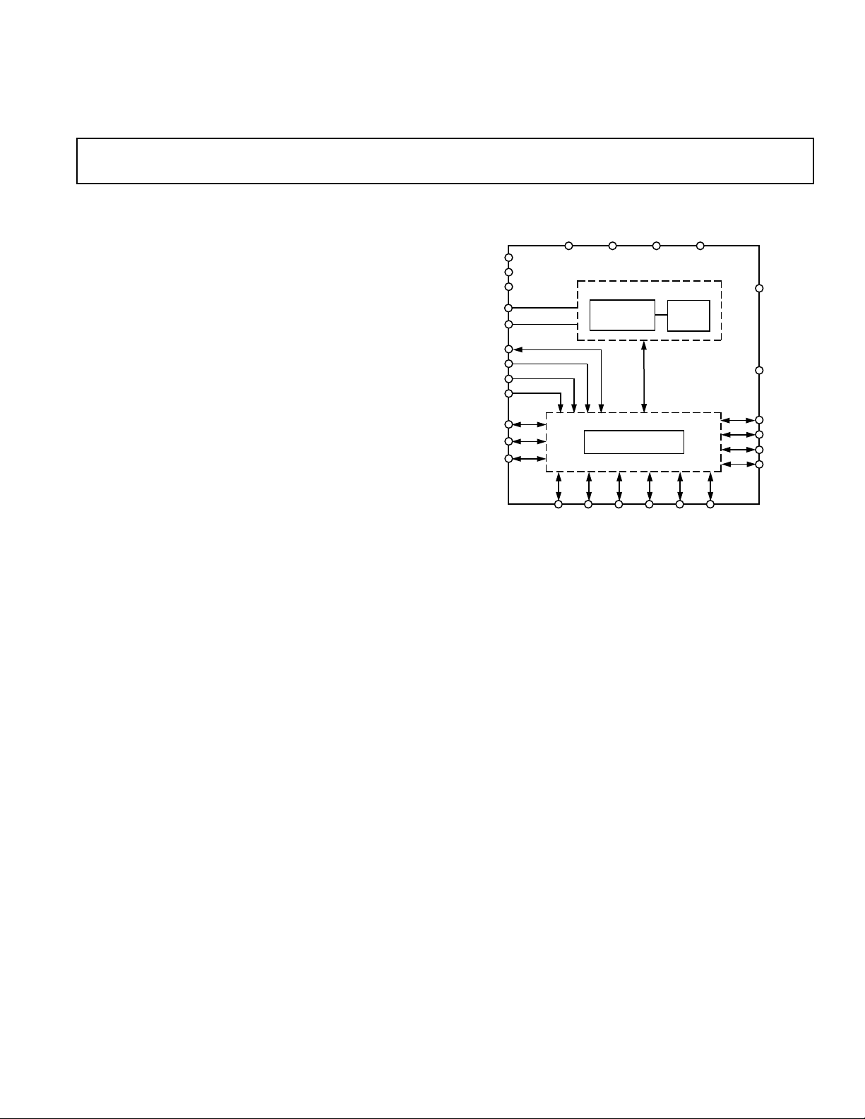
FUNCTIONAL BLOCK DIAGRAM
DD
FIR
FILTER
DB7
DV
DD
REFIN
CLK
DRDY
SDATA/DB11
RFS/DB10
DB9
DB8
S-D
SYNC/
DB5
AV
DB6 SCLK/
DGND
DGND
DSUBST
VIN1
VIN2
DVAL/SYNC
CS
RD
WR
STBY/DB0
CAL/DB1
UNI/DB2
AGND
AD7721
DB3
AGND
12-BIT A/D CONVERTER
MODULATOR
CONTROL LOGIC
DB4
Use of a single bit DAC in the modulator guarantees excellent
linearity and dc accuracy. Endpoint accuracy is ensured by onchip calibration of offset and gain. This calibration procedure
minimizes the part’s zero-scale and full-scale errors.
The output data is accessed from the output register through a
serial or parallel port. This offers easy, high speed interfacing to
modern microcontrollers and digital signal processors. The
serial interface operates in internal clocking (master) mode, the
AD7721 providing the serial clock.
CMOS construction ensures low power dissipation while a
power-down mode reduces the power consumption to only
100 µW.
REV. A
Information furnished by Analog Devices is believed to be accurate and
reliable. However, no responsibility is assumed by Analog Devices for its
use, nor for any infringements of patents or other rights of third parties
which may result from its use. No license is granted by implication or
otherwise under any patent or patent rights of Analog Devices.
One Technology Way, P.O. Box 9106, Norwood, MA 02062-9106, U.S.A.
Tel: 781/329-4700 World Wide Web Site: http://www.analog.com
Fax: 781/326-8703 © Analog Devices, Inc., 1997
Page 2
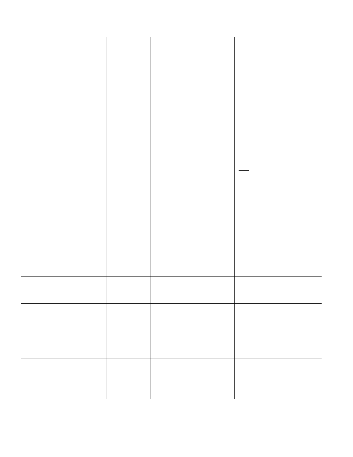
(AVDD = +5 V 6 5%; DVDD = +5 V 6 5%; AGND = DGND = 0 V,
AD7721–SPECIFICA TIONS
1
f
= 15 MHz, REFIN = +2.5 V; TA = T
CLK
MIN
to T
, unless otherwise noted)
MAX
Parameter A Version S Version Units Test Conditions/Comments
SERIAL MODE ONLY
STATIC PERFORMANCE
Resolution 16 16 Bits
Minimum Resolution for Which 12 12 Bits min Guaranteed 12 Bits Monotonic
No Missing Codes Is Guaranteed
Differential Nonlinearity ±8 ±8 LSB typ
Integral Nonlinearity ±16 ± 16 LSB max 16-Bit Operation
DC CMRR 70 70 dB min Bipolar Mode
Offset Error
2
Unipolar Mode ±3.66 ±3.66 mV max Typically 0.61 mV
Bipolar Mode ±3.66 ±3.66 mV max Typically 0.61 mV
Full-Scale Error
2, 3
Unipolar Mode ±4.88 ±4.88 mV max Typically 0.61 mV
Bipolar Mode ±4.88 ±4.88 mV max Typically 1.22 mV
Unipolar Offset Drift 0.05 0.05 mV/°C typ
Bipolar Offset Drift 0.04 0.04 mV/°C typ
ANALOG INPUTS
Signal Input Span (VIN1–VIN2)
Bipolar Mode ±V
Unipolar Mode 0 to V
Maximum Input Voltage AV
/2 ±V
REFIN
REFIN
DD
REFIN
0 to V
AV
DD
/2 Volts max UNI = V
REFIN
Volts max UNI = V
Volts
IH
IL
Minimum Input Voltage 0 0 Volts
Input Sampling Capacitance 1.6 1.6 pF typ
Input Sampling Rate 2 f
CLK
2 f
CLK
MHz Guaranteed by Design
Differential Input Impedance 20.8 20.8 kΩ typ With 15 MHz on CLK Pin
REFERENCE INPUTS
V
REFIN
2.4 to 2.6 2.4 to 2.6 V min/V max
REFIN Input Current 200 200 µA typ
DYNAMIC SPECIFICATIONS
Signal to (Noise + Distortion) 74 74 dB min Input Bandwidth 0 kHz to 210 kHz
Total Harmonic Distortion –78 –78 dB max Input Bandwidth 0 kHz to 229.2 kHz
Frequency Response
0 kHz–210 kHz ±0.05 ±0.05 dB max
229.2 kHz –3 –3 dB min
259.01 kHz to 14.74 MHz –72 –72 dB min
CLOCK
CLK Duty Ratio 45 to 55 45 to 55 % max For Specified Operation
V
, CLK High Voltage 0.7 × DV
CLKH
V
, CLK Low Voltage 0.3 × DV
CLKL
DD
DD
0.7 × DV
0.3 × DV
DD
DD
V min CLK Uses CMOS Logic
V max
LOGIC INPUTS
V
, Input High Voltage 2.0 2.0 V min
INH
V
, Input Low Voltage 0.8 0.8 V max
INL
I
, Input Current 10 10 µA max
INH
CIN, Input Capacitance 10 10 pF max
LOGIC OUTPUTS
, Output High Voltage 4.0 4.0 V min |I
V
OH
VOL, Output Low Voltage 0.4 0.4 V max |I
| ≤ 200 µA
OUT
| ≤ 1.6 mA
OUT
POWER SUPPLIES
AV
DD
DV
DD
I
(Total from AVDD, DVDD) 28.5 28.5 mA max Digital Inputs Equal to 0 V or DV
DD
4.75/5.25 4.75/5.25 V min/V max
4.75/5.25 4.75/5.25 V min/V max
Power Consumption 150 150 mW max Active Mode
Power Consumption 100 100 µW max Standby Mode
NOTES
1
Operating temperature range is as follows: A Version: –40°C to +85°C; S Version: –55°C to +125°C.
2
Applies after calibration at temperature of interest.
3
Full-scale error applies to both positive and negative full-scale error. The ADC gain is calibrated w.r.t. the voltage on the REFIN pin.
Specifications subject to change without notice.
DD
–2–
REV. A
Page 3
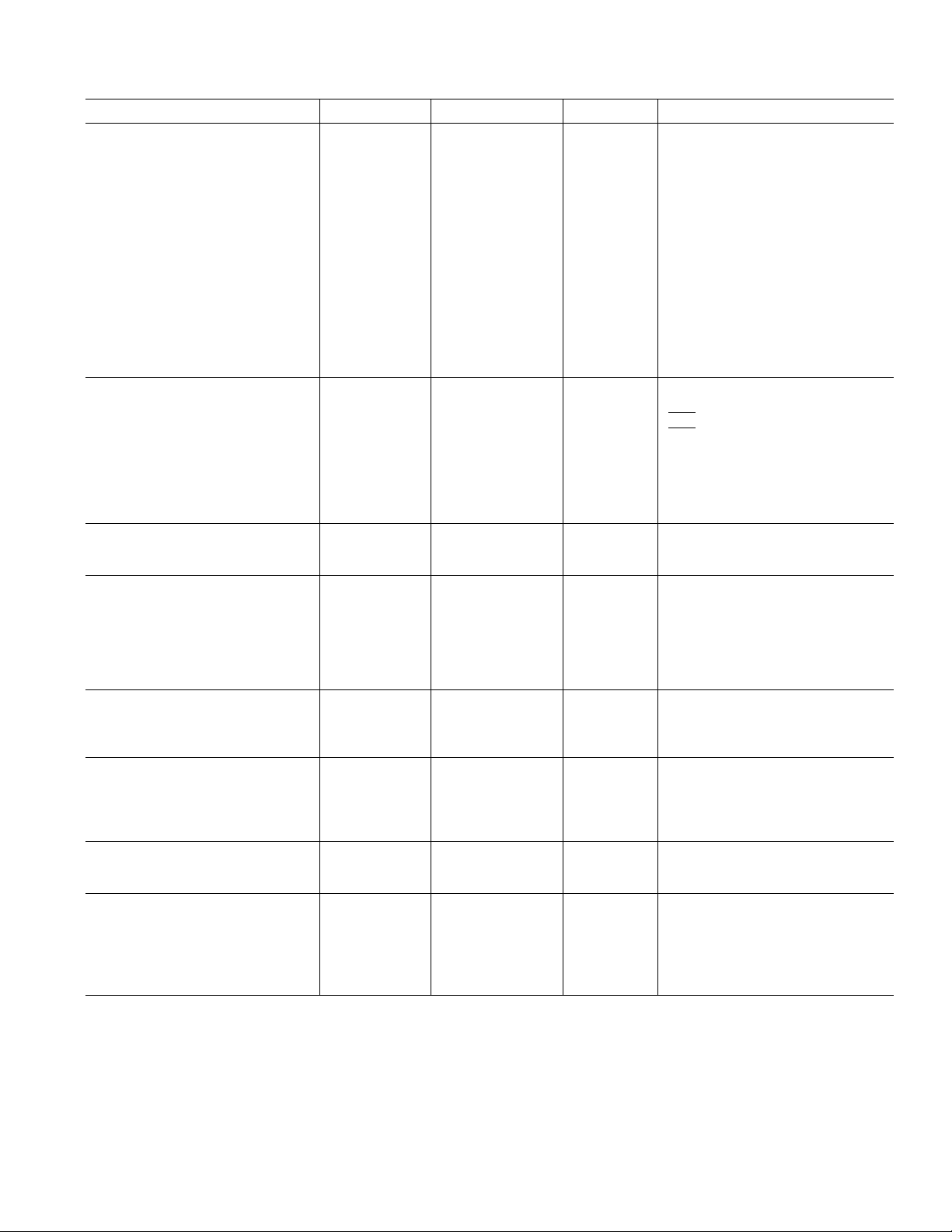
SPECIFICA TIONS
(AVDD = +5 V 6 5%; DVDD = +5 V 6 5%; AGND = DGND = 0 V, f
1
REFIN = +2.5 V; TA = T
MIN
to T
, unless otherwise noted)
MAX
= 10 MHz,
CLK
AD7721
Parameter A Version S Version Units Test Conditions/Comments
PARALLEL MODE ONLY
STATIC PERFORMANCE
Resolution 12 12 Bits
Minimum Resolution for Which 12 12 Bits min Guaranteed 12 Bits Monotonic
No Missing Codes Is Guaranteed
Differential Nonlinearity ±1/2 ±1/2 LSB typ
Integral Nonlinearity ± 1/2 ±1/2 LSB typ 12-Bit Operation
DC CMRR 70 70 dB min Bipolar Mode
Offset Error
2
Unipolar Mode ±3.66 ±3.66 mV max Typically 0.61 mV
Bipolar Mode ±3.66 ±3.66 mV max Typically 0.61 mV
Full-Scale Error
2, 3
Unipolar Mode ±4.88 ±4.88 mV max Typically 0.61 mV
Bipolar Mode ±4.88 ±4.88 mV max Typically 1.22 mV
Unipolar Offset Drift 0.04 0.04 mV/°C typ
Bipolar Offset Drift 0.035 0.035 mV/°C typ
ANALOG INPUTS
Signal Input Span (VIN1–VIN2):
Bipolar Mode ±V
Unipolar Mode 0 to V
Maximum Input Voltage AV
/2 ±V
REFIN
REFIN
DD
0 to V
AV
/2 Volts max UNI = V
REFIN
REFIN
DD
Volts max UNI = V
Volts
IH
IL
Minimum Input Voltage 0 0 Volts
Input Sampling Capacitance 1.6 1.6 pF typ
Input Sampling Rate 2 f
CLK
2 f
CLK
MHz Guaranteed by Design
Differential Input Impedance 31.25 31.25 kΩ typ With 10 MHz on CLK Pin
REFERENCE INPUTS
V
REFIN
2.4 to 2.6 2.4 to 2.6 V min/V max
REFIN Input Current 200 200 µA typ
DYNAMIC SPECIFICATIONS
Signal to (Noise + Distortion) 70 70 dB min Input Bandwidth 0 kHz to 140 kHz
Total Harmonic Distortion –78 –78 dB max Input Bandwidth 0 kHz to 152.8 kHz
Frequency Response
0 kHz–140 kHz ±0.05 ±0.05 dB max
152.8 kHz –3 –3 dB min
172.67 kHz to 9.827 MHz –72 –72 dB min
CLOCK
CLK Duty Ratio 45 to 55 45 to 55 % max For Specified Operation
, CLK High Voltage 0.7 × DV
V
CLKH
V
, CLK Low Voltage 0.3 × DV
CLKL
DD
DD
0.7 × DV
0.3 × DV
DD
DD
V min CLK Uses CMOS Logic
V max
LOGIC INPUTS
, Input High Voltage 2.0 2.0 V min
V
INH
V
, Input Low Voltage 0.8 0.8 V max
INL
, Input Current 10 10 µA max
I
INH
CIN, Input Capacitance 10 10 pF max
LOGIC OUTPUTS
, Output High Voltage 4.0 4.0 V min |I
V
OH
V
, Output Low Voltage 0.4 0.4 V max |I
OL
| ≤ 200 µA
OUT
| ≤ 1.6 mA
OUT
POWER SUPPLIES
AV
DD
DV
DD
(Total from AVDD, DVDD) 28.5 28.5 mA max
I
DD
4.75/5.25 4.75/5.25 V min/V max
4.75/5.25 4.75/5.25 V min/V max
Digital Inputs Equal to 0 V or DV
Power Consumption 150 150 mW max Active Mode
Power Consumption 100 100 µW max Standby Mode
NOTES
1
Operating temperature range is as follows: A Version: –40° C to +85°C; S Version: –55 °C to +125 °C.
2
Applies after calibration at temperature of interest.
3
Full-scale error applies to both positive and negative full-scale error. The ADC gain is calibrated w.r.t. the voltage on the REFIN pin.
Specifications subject to change without notice.
DD
REV. A
–3–
Page 4
AD7721
TIMING CHARACTERISTICS
(AVDD= +5 V 6 5%; DVDD= +5 V 6 5%; AGND = DGND = 0 V, REFIN= +2.5 V
1, 2
unless otherwise noted)
Limit at T
MIN
, T
MAX
Parameter (A, S Versions) Units Conditions/Comments
Serial Interface
3
f
CLK
100 kHz min Master Clock Frequency
15 MHz max 15 MHz for Specified Performance
t
CLK LO
t
CLK HI
t
1
4
t
2
t
3
t
4
t
5
t
6
t
7
5
t
8
0.45 × t
0.45 × t
t
t
CLK
CLK
CLK
– 10 ns min RFS Low to SCLK Falling Edge Setup Time
CLK HI
ns min Master Clock Input Low Time
ns min Master Clock Input High Time
ns nom DRDY High Time
20 ns max RFS Low to Data Valid Delay
t
CLK HI
t
CLK LO
ns nom SCLK High Pulse Width
ns nom SCLK Low Pulse Width
25 ns max SCLK Rising Edge to Data Valid Delay
0 ns min RFS to SCLK Falling Edge Hold Time
0 ns min Bus Relinquish Time after Rising Edge of RFS
20 ns max
t
9
Parallel Interface
3
f
CLK
32 × t
CLK
ns nom Period between Consecutive DRDY Rising Edges
100 kHz min Master Clock Frequency
10 MHz max 10 MHz for Specified Performance
t
CLK LO
t
CLK HI
0.45 × t
0.45 × t
CLK
CLK
ns min Master Clock Input Low Time
ns min Master Clock Input High Time
Read Operation
t
10
t
11
t
12
2 × t
CLK
ns nom DRDY High Time
30 ns max Data Access Time after Falling Edge of DRDY
32 × t
CLK
ns nom Period between Consecutive DRDY Rising Edges
Write Operation
t
13
t
14
t
15
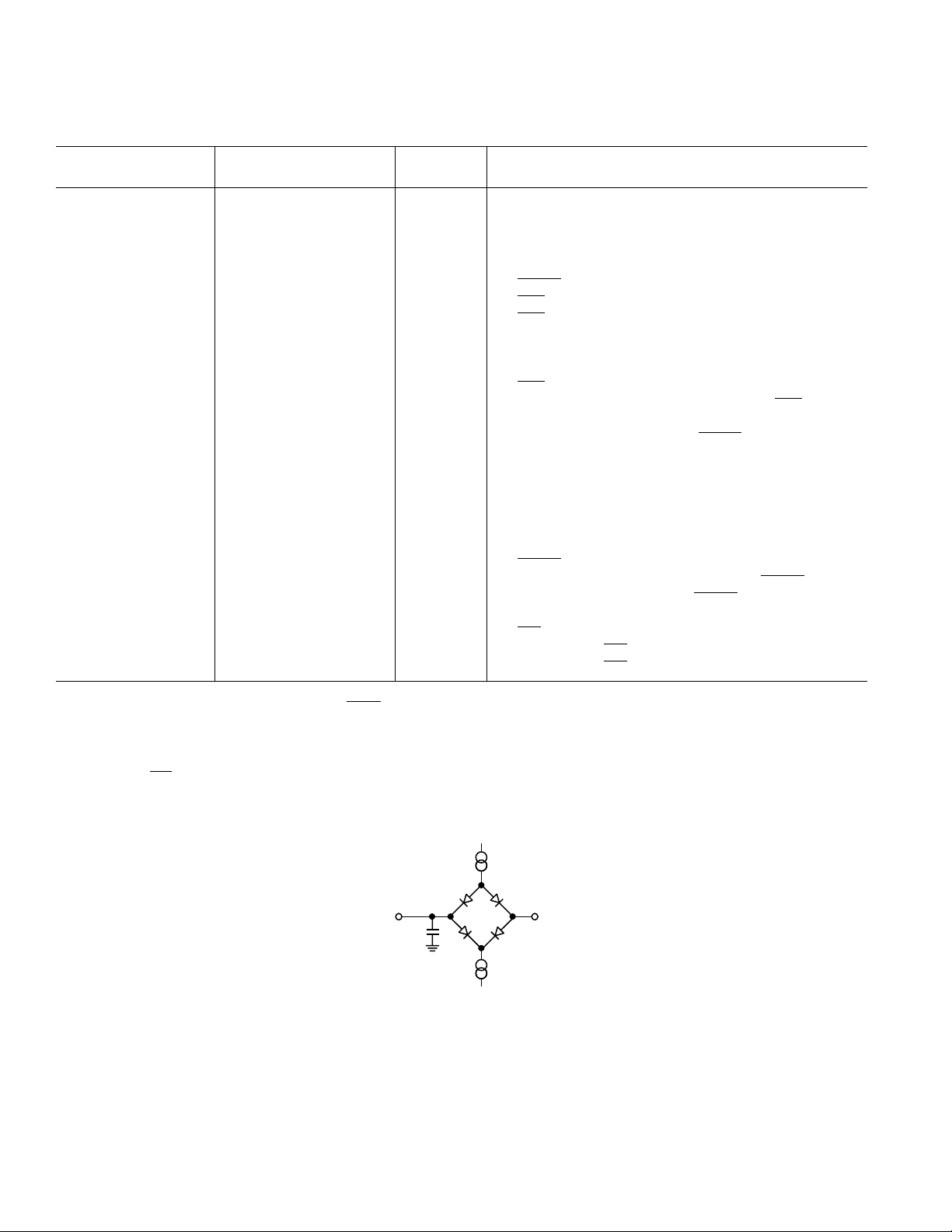
NOTES
The timing is measured with a load of 50 pF on SCLK and DRDY . SCLK can be operated with a load capacitance of 50 pF maximum.
1
Sample tested at +25°C to ensure compliance. All input signals are specified with tr = tf = 5 ns (10% to 90% of 5 V) and timed from a voltage level of 1.6 V.
2
All digital outputs are timed with the load circuit below and, except for t2, are defined as the time required for an output to cross 0.8 V or 2 V, whichever occurs last.
3
The AD7721 is production tested with f
ization to operate with CLK frequencies down to 100 kHz.
4
t2 is the time from RFS crossing 1.6 V to SCLK crossing 0.8 V.
5
t8 and t15 are derived from the measured time taken by the data outputs to change 0.5 V when loaded with the circuit shown below. The measured number is then
extrapolated back to remove the effects of charging or discharging the 50 pF capacitor. This means that the time quoted in the Timing Characteristics is the true bus
relinquish time of the part and, as such, is independent of external bus loading capacitance.
35 ns min WR Pulse Width
20 ns min Data Valid to WR High Setup Time
0 ns min Data Valid to WR High Hold Time
at 10 MHz for parallel mode operation and at 15 MHz for serial mode operation. However, it is guaranteed by character-
CLK
1.6mA
I
OL
TO
OUTPUT
PIN
50pF
C
L
200mA
I
OH
+1.6V
Figure 1. Load Circuit for Access Time and Bus Relinquish Time
–4–
REV. A
Page 5
AD7721
ABSOLUTE MAXIMUM RATINGS
(TA = +25°C unless otherwise stated)
DVDD to DGND . . . . . . . . . . . . . . . . . . . . . . . –0.3 V to +7 V
AV
to AGND . . . . . . . . . . . . . . . . . . . . . . . –0.3 V to +7 V
DD
AV
to DVDD . . . . . . . . . . . . . . . . . . . . . . –0.3 V to +0.3 V
DD
AGND to DGND . . . . . . . . . . . . . . . . . . . . –0.3 V to +0.3 V
Digital Input Voltage to DGND . . . –0.3 V to DV
Analog Input Voltage to AGND . . . . –0.3 V to AV
Input Current to Any Pin Except Supplies
Operating Temperature Range
Industrial (A Version) . . . . . . . . . . . . . . . . . –40°C to +85°C
Extended (S Version) . . . . . . . . . . . . . . . . –55°C to +125°C
Storage Temperature Range . . . . . . . . . . . . –65°C to +150°C
Maximum Junction Temperature . . . . . . . . . . . . . . . +150°C
Plastic Package
θ
Thermal Impedance . . . . . . . . . . . . . . . . . . . . . 74°C/W
JA
1
2
. . . . . . . ±10 mA
+ 0.3 V
DD
+ 0.3 V
DD
Lead Temperature, Soldering (10 sec) . . . . . . . . . . +260°C
Cerdip Package
θ
Thermal Impedance . . . . . . . . . . . . . . . . . . . . . 51°C/W
JA
Lead Temperature, Soldering (10 sec) . . . . . . . . . . +300°C
SOIC Package
θ
Thermal Impedance . . . . . . . . . . . . . . . . . . . . . 72°C/W
JA
Lead Temperature, Soldering
Vapor Phase (60 sec) . . . . . . . . . . . . . . . . . . . . . . +215°C
Infrared (15 sec) . . . . . . . . . . . . . . . . . . . . . . . . . +220°C
NOTES
1
Stresses above those listed under Absolute Maximum Ratings may cause perma-
nent damage to the device. This is a stress rating only; functional operation of the
device at these or any other conditions above those listed in the operational
sections of this specification is not implied. Exposure to absolute maximum
rating conditions for extended periods may affect device reliability.
2
Transient currents of up to 100 mA will not cause SCR latchup.
CAUTION
ESD (electrostatic discharge) sensitive device. Electrostatic charges as high as 4000 V readily
accumulate on the human body and test equipment and can discharge without detection.
Although this device features proprietary ESD protection circuitry, permanent damage may
occur on devices subjected to high energy electrostatic discharges. Therefore, proper ESD
precautions are recommended to avoid performance degradation or loss of functionality.
WARNING!
ESD SENSITIVE DEVICE
ORDERING GUIDE
Model Temperature Range Package Option*
AD7721AN –40°C to +85°C N-28
AD7721AR –40°C to +85°C R-28
AD7721SQ –55°C to +125°C Q-28
*N = Plastic DIP; R = 0.3" Small Outline IC (SOIC); Q = Cerdip.
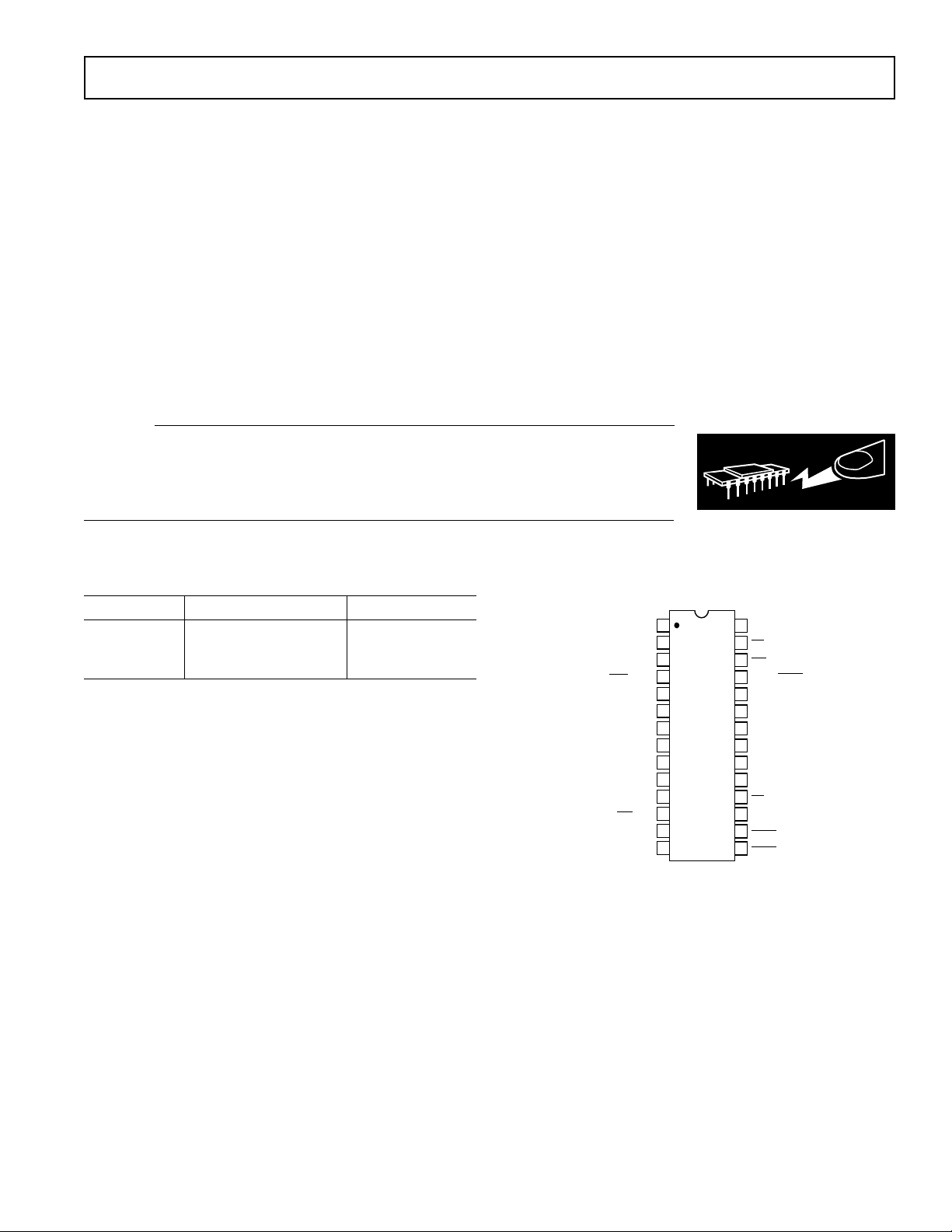
PIN CONFIGURATION
SCLK/DB7
RFS
SDATA/DB11
STBY/DB0
DB8
DB9
/DB10
DGND
DSUBST
DGND
DV
CAL/DB1
UNI
/DB2
DB3
DB4
DD
1
2
3
4
5
AD7721
6
TOP VIEW
(Not to Scale)
7
8
9
10
11
12
13
14
DB6
28
27
RD
26
WR
25
DVAL/SYNC
AGND
24
23
VIN2
VIN1
22
REFIN
21
20
AGND
19
AV
18
CS
17
CLK
16
DRDY
15
SYNC/DB5
DD
REV. A
–5–
Page 6

AD7721
PIN FUNCTION DESCRIPTIONS
Mnemonic Function
AV
DD
AGND Ground reference point for analog circuitry.
DV
DD
DGND Ground reference point for digital circuitry. DGND must be connected via its own short path to AGND (Pin 24).
DSUBST This is the substrate connection for digital circuits. It must be connected via its own short path to AGND
VIN1 Analog Input. In unipolar operation, the analog input range on VIN1 is VIN2 to (VIN2 + V
VIN2 operation, the analog input range on VIN1 is (VIN2 ± V
REFIN Reference Input. The AD7721 operates with an external reference, of value 2.5 V nominal. A suitable refer-
CLK CMOS Logic Clock Input. The AD7721 operates with an external clock which is connected to the CLK pin.
Serial Mode Only
CS, RD, WR To select the serial interface mode of operation, the AD7721 must be powered up with CS, RD and WR all
DRDY In the serial interface mode, a rising edge on DRDY indicates that new data is available to be read from the
SDATA/DB11 Serial Data Output. Output serial data becomes active after
RFS/DB10 Receive Frame Synchronization. Active low logic input. This is a logic input with RFS provided by connect-
DB9 This is a test mode pin. This pin must be tied to DGND.
DB8 This is a test mode pin. This pin must be tied to DGND.
SCLK/DB7 Serial Clock. Logic Output. The internal digital clock is provided as an output on this pin. Data is output
DB6 This is a test mode pin. This pin must be tied to DGND.
SYNC/DB5 Synchronization Logic Input. A rising edge on SYNC starts the synchronization cycle. SYNC must be
DB4 This is a test mode pin. This pin must be tied to DGND.
DB3 This is a test mode pin. This pin must be tied to DGND.
UNI/DB2 Analog Input Range Select, Logic Input. A logic low on this input selects unipolar mode. A logic high selects
CAL/DB1 Calibration Mode Logic Input. CAL must go high for at least one clock cycle to initiate a calibration cycle.
STBY/DB0 Standby Mode Logic Input. A logic high on this pin selects standby mode.
DVAL/SYNC Data Valid Digital Output. In serial mode, this pin is a dedicated data valid pin.
Analog Positive Supply Voltage, +5 V ± 5%.
Digital Supply Voltage, +5 V ± 5%.
(Pin 24).
); for bipolar
REFIN
between 0 and AV
/2). The absolute analog input range must lie
. The analog input is continuously sampled and processed by the analog modulator.
DD
REFIN
ence for operation with the AD7721 is the AD780. A 100 nF decoupling capacitor is required between
REFIN and AGND.
The modulator samples the analog input on both phases of the clock, increasing the sampling rate to 20 MHz
(CLK = 10 MHz) or 30 MHz (CLK = 15 MHz).
tied to DGND. After two clock cycles, the AD7721 switches into serial mode. These pins must remain low
during serial operation.
interface. During a synchronization or calibration cycle,
DRDY remains low until valid data is available.
RFS goes low. Sixteen bits of data are clocked
out starting with the MSB. Serial data is clocked out on the rising edge of SCLK and is valid on the subsequent falling edge of SCLK.
ing this input to
DRDY. When RFS is high, SDATA is high impedance.
from the AD7721 on the rising edge of SCLK and is valid on the falling edge of SCLK.
pulsed low for at least one clock cycle to initiate a synchronization cycle.
bipolar mode.
–6–
REV. A
Page 7

AD7721
Parallel Mode Only
Mnemonic Function
CS Chip Select Logic Input.
RD Read Logic Input. This digital input is used in conjunction with CS to read data from the device.
WR Write Logic Input. This digital input is used in conjunction with CS to write data to the control register.
DRDY In parallel interface mode, a falling edge on DRDY indicates that new data is available to be read from the
interface. During a synchronization or calibration cycle,
SYNC The function of this pin is determined by the state of bit DB3 in the control register. Writing a logic zero to
DVAL/
bit DB3 will program this pin to be a DVAL output. Writing a logic one to bit DB3 will program this pin to
be a
SYNC input pin.
A rising edge on
cycle.
When switching this pin from
the pin which could cause resynchronization. For this purpose, an internal pull-up resistor has been included
on this pin. Thus, when the external driver driving this pin in
pin remains high.
SDATA/DB11– These pins are both data outputs and control register inputs. Output data is placed on these pins by taking
STBY/DB0
RD and CS low. Data on these pins is read into the control register by toggling WR low with CS low. With
RD high, these pins are high impedance.
SYNC starts the synchronization cycle. SYNC must be pulsed low for at least one clock
SYNC mode to DVAL mode, it is important that there are no rising edges on
DRDY remains high until valid data is available.
SYNC mode is switched off, the DVAL/SYNC
Control functions such as CAL,
Table I lists the contents of the control register onboard the AD7721. This register is written to in parallel mode using the
Control
Register Logical
Bit Function State Mode
DB0 STBY 0 Normal Operation.
DB1 CAL 0 Normal Operation.
DB2 UNI 0 Unipolar Mode.
DB3 DVAL/SYNC 0 Sets DVAL/SYNC Pin to DVAL Mode.
DB9 0 This bit is used for testing the AD7721. A logic low MUST be written into this bit for normal
UNI and STBY, which are available as pins in serial mode, are available as bits in parallel mode.
WR pin.
Table I. Function of Control Register Bits
1 Power-Down (Standby) Mode.
1 Writing a Logic “1” to this bit starts a calibration cycle. Internal logic resets this bit to zero at the end of
calibration.
1 Bipolar Mode.
1 Sets DVAL/SYNC Pin to SYNC Mode.
operation.
REV. A
–7–
Page 8

AD7721
TERMINOLOGY
Integral Nonlinearity
This is the maximum deviation of any code from a straight line
passing through the endpoints of the transfer function. The endpoints of the transfer function are zero scale (not to be confused with bipolar zero), a point 0.5 LSB below the first code
transition (100 . . . 00 to 100. . . 01 in bipolar mode and
000 . . . 00 to 000 . . . 01 in unipolar mode) and full scale, a point
0.5 LSB above the last code transition (011 . . . 10 to 011 . . . 11 in
bipolar mode and 111 . . . 10 to 111. . . 11 in unipolar mode). The
error is expressed in LSBs.
Differential Nonlinearity
This is the difference between the measured and the ideal 1 LSB
change between two adjacent codes in the ADC.
Common Mode Rejection Ratio
The ability of a device to reject the effect of a voltage applied to
both input terminals simultaneously—often through variation of
a ground level—is specified as a common-mode rejection ratio.
CMRR is the ratio of gain for the differential signal to the gain
for the common-mode signal.
Unipolar Offset Error
Unipolar offset error is the deviation of the first code transition
from the ideal VIN1 voltage which is (VIN2 + 0.5 LSB) when
operating in the unipolar mode.
Bipolar Offset Error
This is the deviation of the midscale transition (111. . . 11
to 000 . . . 00) from the ideal VIN1 voltage which is (VIN2 –
0.5 LSB) when operating in the bipolar mode.
Unipolar Full-Scale Error
Unipolar full-scale error is the deviation of the last code transition
(111 . . . 10 to 111 . . . 11) from the ideal VIN1 voltage which is
(VIN2 + V
– 3/2 LSBs).
REFIN
Bipolar Full-Scale Error
The bipolar full-scale error refers to the positive full-scale error and
the negative full-scale error. The positive full-scale error is the
deviation of the last code transition (011 . . . 10 to 011 . . . 11) from
the ideal VIN1 voltage which is (VIN2 + V
/2 – 3/2 LSB).
REFIN
The negative full-scale error is the deviation of the first code transition (100 . . . 00 to 100 . .. 01) from the ideal VIN1 voltage which
is (VIN2 – V
/2 + 0.5 LSB).
REFIN
Signal to (Noise + Distortion)
Signal to (Noise + Distortion) is measured signal to noise at the
output of the ADC. The signal is the rms magnitude of the fundamental. Noise is the rms sum of all the nonfundamental signals up
to half the sampling frequency (f
/2) but excluding the dc com-
CLK
ponent. Signal to (Noise + Distortion) is dependent on the number of quantization levels used in the digitization process; the more
levels, the smaller the quantization noise. The theoretical Signal to
(Noise + Distortion) ratio for a sine wave input is given by
Signal to (Noise + Distortion) = (6.02 N + 1.76) dB
where N is the number of bits. Thus, for an ideal 12-bit converter,
Signal to (Noise + Distortion) = 74 dB.
Total Harmonic Distortion
Total Harmonic Distortion (THD) is the ratio of the rms sum
of harmonics to the rms value of the fundamental. For the
AD7721, THD is defined as
where V1 is the rms amplitude of the fundamental and V2, V3,
V
, V5 and V6 are the rms amplitudes of the second through the
4
sixth harmonic.
USING THE AD7721
ADC Differential Inputs
The AD7721 uses differential inputs to provide common-mode
noise rejection. In the bipolar mode configuration, the analog
input range is ±1.25 V. The designed code transitions occur
midway between successive integer LSB values. The output
code is 2s complement binary with 1 LSB = 0.61 mV in parallel mode and 38 µV in serial mode. The ideal input/output
transfer function is illustrated in Figure 2.
In the unipolar mode, the analog input range is 0 V to 2.5 V.
Again, the designed code transitions occur midway between successive integer LSB values. The output code is straight binary with
1 LSB = 0.61 mV in parallel mode and 38 µV in serial mode. The
ideal input/output transfer function is shown in Figure 3.
OUTPUT
CODE
011...111
011...110
000...010
000...001
000...000
111...111
111...110
100...001
100...000
AD7721
–REF IN/2
DIFFERENTIAL INPUT VOLTAGE (VIN1–VIN2)
0V
+REF IN/2–1LSB
Figure 2. AD7721 Bipolar Mode Transfer Function
OUTPUT
CODE
111...111
111...110
111...101
111...100
000...011
000...010
000...001
000...000
AD7721
0V REF IN–1LSB
DIFFERENTIAL INPUT VOLTAGE (VIN1–VIN2)
THD = 20 log
(V
2
2
2
2
+V
+V
2
3
+V
4
V
1
2
+V
5
)
6
Figure 3. AD7721 Unipolar Mode Transfer Function
–8–
REV. A
Page 9

AD7721
Input Circuits
The purpose of antialiasing filters is to attenuate out of band
signals that would otherwise be mixed down into the signal
band. With traditional ADCs, high order filters using expensive
high tolerance passive components are often required to perform this function. Using oversampling, as employed on the
AD7721, this problem is considerably alleviated. Figure 4a
shows the digital filter frequency response. Due to the sampling
nature of the digital filter, the passband is repeated about the
operating clock frequency and at multiples of the clock frequency. Out of band signals coincident with any of the filter
images are mixed down into the passband. Figure 4b shows the
frequency response of the antialias filter required to provide a
particular level of attenuation at the first image frequency. Figure 4c shows the frequency response of the antialias filter required to achieve the same level of attenuation with a traditional
ADC. The much smaller transition band can only be achieved
with a very high order filter.
0dB
f
CLK
2
f
CLK
3
f
CLK
a. Digital Filter Frequency Response
OUTPUT DATA RATE
0dB
ANTIALIAS FILTER
RESPONSE
f
CLK
REQUIRED
ATTENUATION
b. Frequency Response of Antialias Filter (AD7721)
The choice of the filter corner frequency will depend on the
amount of rolloff which is acceptable in-band and the attenuation which is required at the first image frequency. For example,
when f
= 15 MHz, R
CLK
= 50 Ω, C
EXT
= 7.84 nF, the in-
EXT
band rolloff is 1 dB and the attenuation at the first image frequency is 31.1 dB. Increasing the size of the external resistor
above 50 Ω can cause increased distortion due to nonlinear
charging currents.
R
ANALOG
INPUT
EXT
C
EXT
R
EXT
C
EXT
VIN1
AD7721
VIN2
Figure 5. Simple RC Antialiasing Filter
Figure 6 shows a simple circuit that can be used to drive the
AD7721 in unipolar mode. The input of the AD7721 is sampled
by a 1.6 pF input capacitor. This creates glitches on the input
of the modulator. By placing the RC filter directly before the
AD7721, rather than before the operational amplifier, these
glitches are prevented from being fed back into the operational
amplifier and creating distortion. The resistor in this diagram,
as well as creating a pole for the antialias filter, also isolates the
storage capacitor from the operational amplifier which may
otherwise be unstable.
ANALOG
INPUT
COMMON
MODE
VOLTAGE
R
EXT
C
EXT
VIN1
AD7721
VIN2
ANTIALIAS FILTER
RESPONSE
0dB
OUTPUT DATA RATE
REQUIRED
ATTENUATION
c. Frequency Response of Antialias Filter (Traditional ADC)
Figure 4. Frequency Response of Antialiasing Filters
Figure 5 shows a simple antialiasing filter which can be used
with the AD7721. The –3 dB corner frequency (f
3dB
) of the
antialias filter is given by Equation 1, and the attenuation of the
filter is given by Equation 2. Attenuation at the first image
frequency is given by Equation 3.
f
= 1/(2 π R
3 dB
EXT CEXT
Attenuation = 20 log
) Equation 1
1/ 1+ f / f
()
3dB
2
Equation 2
Attenuation (First Image)=
20log 1/ 1+ 0.986f
()
CLK
/ f
2
3dB
Equation 3
Figure 6. Antialiasing Circuits
A suitable operational amplifier is the AD847 if a ± 15 V power
supply is available. If only a +5 V power supply is available, the
AD820 can be used. This operational amplifier can be used with
input bandwidths up to 80 kHz. However, the slew rate of this
operational amplifier limits its performance to 80kHz. Above
this frequency, the performance of the AD820 degrades.
For both filters, the capacitor C
should have a low tempera-
EXT
ture coefficient and should be linear to avoid distortion.
Polypropylene or polystyrene capacitors are suitable.
Offset and Gain Calibration
A calibration of offset and gain errors can be performed in both
serial and parallel modes by initiating a calibration cycle. During
this cycle, offset and gain registers in the filter are loaded with
values representing the dc offset of the analog modulator and a
modulator gain correction factor. In normal operation, the offset
register is subtracted from the digital filter output and this result
is then multiplied by the gain correction factor to obtain an
offset and gain corrected final result.
During the calibration cycle, in which the offset of the analog
modulator is evaluated, the inputs to the modulator are shorted
together internally. When the modulator and digital filter settle,
the average of 8 output results is calculated and stored in the
offset register. The gain of the modulator is determined by
REV. A
–9–
Page 10

AD7721
switching the positive input of the modulator to the reference
voltage and the negative input to AGND. Again, when the
modulator and digital filter settle, a gain correction factor is
calculated from the average of 8 output results and stored in the
gain register. After the calibration registers have been loaded
with new values, the inputs of the modulator are switched back
to the input pins. However, correct data is available at the interface only after the modulator and filter have settled to the new
input values.
The whole calibration cycle is controlled by internal logic, and the
controller need only initiate the cycle. The calibration values
loaded into the registers only apply for the particular analog input
mode (bipolar/unipolar) selected when initiating the calibration
cycle. On changing to a different analog input mode, a new calibration must be performed. The duration of the calibration cycle is up
to 6720 clock cycles for the unipolar mode and up to 9024 clock
cycles for the bipolar mode. Until valid data is available at the
interface, the
serial mode. Should the part see a rising edge on the
serial mode or on the DVAL/
DRDY pin remains high in parallel mode and low in
SYNC pin in
SYNC pin (if programmed as a
SYNC pin), then the calibration cycle is discontinued and a syn-
chronization operation will be performed. Similarly, putting the
part into standby mode during the cycle will discontinue the calibration cycle.
The calibration registers are static and retain their contents even
during standby. They need to be updated only if unacceptable
drifts in analog offsets or gain are expected. On power-up in
parallel mode, the offset and gain errors may contain incorrect
values and therefore a calibration must be performed at least
once after power-up. In serial mode, a calibration on power-up
is not mandatory if the CAL pin is grounded prior to power-up
as the calibration register will be reset to zero. Before initiating a
calibration routine, ensure that the supplies have settled and that
the voltage on the analog input pins is between the supply voltages.
Calibration does not affect the synchronization of the part.
Synchronization
Data is presented at the interface at 1/32 the CLK frequency. In
order that this data is presented to the interface at a known
point in time or to ensure that the data from more than one
device is a filtered and decimated result derived from the same
input samples, a synchronizing function has been provided. In
parallel mode, the DVAL/
a
SYNC pin by writing to the control register. In serial mode,
there is a dedicated
pulse or the DVAL/
known state. For 2080 clock cycles,
parallel mode and low in serial mode. When
SYNC pin must first be configured as
SYNC pin. On the rising edge of the SYNC
SYNC pulse, the digital filter is reset to a
DRDY remains high in
DRDY changes
state at the end of this period, valid data is available at the interface. Synchronizing the part has no affect on the values in the
calibration register.
SYNC is latched internally on the rising edge of DCLK which is
a delayed version of the clock on the CLK pin. Should
SYNC
go high coincidentally with DCLK, there is a potential uncertainty of one clock cycle in the start of the synchronization cycle.
To avoid this,
SYNC should be taken high after the falling edge
of the clock on the CLK pin and before the rising edge of this
clock.
Standby
The part can be put into a low power standby mode by writing
to the configuration register in parallel mode or by taking the
STBY pin high in serial mode. During Standby, the clock to
both the modulator and the digital filter is turned off and bias is
removed from all analog circuits. On coming out of standby
mode, the
serial mode for 2080 clock cycles. When
DRDY pin remains high in parallel mode and low in
DRDY changes state,
valid data is available at the interface. As soon as the part is
taken out of standby mode, a synchronization or calibration
cycle can be initiated.
DVAL
The DVAL pin or the DVAL/SYNC pin, when programmed as
a DVAL pin, is used to indicate that an overrange input signal
has resulted in invalid data at the ADC output. Small overloads
will result in DVAL going low and the output being clipped to
positive or negative full scale, depending on the sign of the
overload. As with all single bit DAC high order sigma-delta
modulators, large overloads on the inputs can cause the modulator to go unstable. The modulator is designed to be stable with
signals within the input bandwidth that exceed full scale by
20%. When instability is detected by internal circuits, the
modulator is reset to a stable state and DVAL is held low for
2080 clock cycles. During this period, the output registers are
set to negative full scale. Whenever DVAL goes low,
DRDY will
continue to indicate that there is data to be read.
Varying the Master Clock Frequency
The AD7721 can be operated with clock frequencies less than
10 MHz. The sample rate, output word rate and cutoff frequency of the FIR filters are directly proportional to the master
clock frequency. The analog input is sampled at a frequency of
2f
while the output word rate equals f
CLK
/32. For example,
CLK
reducing the clock frequency to 5 MHz leads to a sample frequency of 10 MHz, an output word rate of 156.25 kHz and a
corner frequency of 76.4 kHz. The AD7721 can be operated
with clock frequencies down to 100 kHz.
Power Supply Sequencing
If separate analog and digital supplies are used, care must be
taken to ensure that both supplies remain within ± 0.3 V of each
other both during normal operation and during power-up and
power-down to completely eliminate the possibility of latch-up.
If this cannot be assured, then the protection circuit shown in
Figure 7 is recommended. The 10 Ω resistors may be required to
limit the current through the diodes if particularly fast edges are
expected on the supplies during power-up and power-down.
If only one supply is available, then DV
must be connected to
DD
the analog supply. Supply decoupling capacitors are still required as close as possible to both supply pins.
IN4148
10V10V
1mF
1mF
10nF
AV
DD
IN4148
AD7721
DV
DD
10nF
Figure 7. Powering-Up Protection Scheme
–10–
REV. A
Page 11

AD7721
0.0
–50.0
–100.0
–150.0
1.0f
CLK
/320.8f
CLK
/320.6f
CLK
/320.4f
CLK
/320.2f
CLK
/320.0f
CLK
/32
FREQUENCY
GAIN – dB
CIRCUIT DESCRIPTION
Sigma-Delta ADC
The AD7721 ADC employs a sigma-delta conversion technique
that converts the analog input into a digital pulse train.
Due to the high oversampling rate, which spreads the quantization noise from 0 to f
/2, the noise energy which is contained
CLK
in the band of interest is reduced (Figure 8a). To reduce the
quantization noise further, a high order modulator is employed
to shape the noise spectrum, so that most of the noise energy is
shifted out of the band of interest (Figure 8b).
The digital filter that follows the modulator removes the large
out of band quantization noise (Figure 8c), while converting the
digital pulse train into parallel 12 bit wide binary data or serial
16 bit wide binary data.
QUANTIZATION NOISE
BAND OF
INTEREST
f
/2
CLK
a.
a linear phase response. This is very difficult to achieve with
analog filters.
Analog filters, however, can remove noise superimposed on the
signal before it reaches the ADC. Digital filtering cannot do this
and noise peaks riding on signals, near full-scale, have the potential to overload the analog modulator even though the average value of the signal is within limits.
0.0
–50.0
GAIN – dB
–100.0
–150.0
0.0f
CLK
0.1f
CLK
0.2f
CLK
FREQUENCY
0.3f
CLK
0.4f
CLK
0.5f
CLK
Figure 9a. 128 Tap FIR Filter Frequency Response
NOISE
SHAPING
BAND OF
INTEREST
f
/2
CLK
b.
DIGITAL FILTER CUTOFF FREQUENCY
WHICH EQUALS 152.8kHz (10MHz) OR
229.2kHz (15MHz)
BAND OF
INTEREST
f
/2
CLK
c.
Figure 8. Sigma-Delta ADC
Digital Filter
The digital filter that follows the modulator removes the large
out of band quantization noise, while converting the one bit
digital pulse train into 12-bit or 16-bit wide binary data. The
digital filter also reduces the data rate from f
the filter to f
/32 at the output of the filter. The output data
CLK
at the input of
CLK
rate is a little over twice the signal bandwidth which guarantees
that there is no loss of data in the signal band.
The AD7721 employs 2 FIR filters in series. The first filter is a
128 tap filter that samples the output of the modulator at f
The second filter is an 83 tap half-band filter that samples the
output of the first filter at f
/16 and decimates by 2. The
CLK
frequency response of the 2 filters is shown in Figure 9.
Digital filtering has certain advantages over analog filtering.
First, since digital filtering occurs after the A/D conversion, it
can remove noise injected during the conversion process. Analog filtering cannot do this. Second, the digital filter combines
low passband ripple with a steep roll off, while also maintaining
REV. A
CLK
Figure 9b. 83 Tap FIR Filter Frequency Response
SERIAL INTERFACE
The AD7721’s serial communication port allows easy interfacing to industry-standard microprocessors, microcontrollers
and digital signal processors. The AD7721 is operated in selfclocking mode, the AD7721 providing the serial clock. The
RFS signal is also provided by the AD7721 by tying RFS to
DRDY.
Figure 10 shows the timing diagram for reading from the
AD7721.
been completed.
.
(15 MHz) cycle and then goes low for the next 31 clock cycles.
DRDY goes high to indicate that a conversion has
DRDY remains high for one internal clock
New data is loaded into the output shift register on the rising
edge of
DRDY. When DRDY goes low, the data is accessed
from the AD7721. Although the AD7721 has a 12-bit digital
output in the parallel mode, sixteen bits of data are available for
transmission in the serial mode, starting with the MSB. Serial
data is clocked out of the device on the rising edge of SCLK
and is valid on the falling edge of SCLK.
–11–
Page 12

AD7721
PARALLEL INTERFACE
Read Operation
The device defaults to parallel mode if CS, RD and WR are not
tied to DGND together. Figure 11 shows a timing diagram for
reading from the AD7721 in the parallel mode. When operating
the device in parallel mode,
CS and RD should be tied to
DGND permanently except when control information is being
written to the AD7721.
DRDY goes high for 2 clock cycles to
indicate that new data is available from the interface. The
AD7721 outputs this data after the falling edge of
DRDY. This
DRDY pin can be used to drive an edge-triggered interrupt of a
microprocessor.
t
RFS (I) / DRDY (O)
SCLK (O)
DATA OUT (O)
NOTE: (I) SIGNIFIES AN INPUT; (O) SIGNIFIES AN OUTPUT.
1
t
2
t
3
t
4
t
5
Figure 10. Serial Mode Output Register Read
CS (I)
Write Operation
The write operation is used to write data into the control register. The outputs of the control register select the analog input
range, allow the part to be put into power-down (standby)
mode, define the function of the DVAL/
SYNC pin, and initiate
the calibration routine. After power-up and after at least 16
clock cycles, the control register must be written to. A calibration must also be performed at least once after power-up to
set the calibration registers. The function of each bit in the
control register is shown in Table I. When writing to the control register, the
RD pin must be taken high so that the pins D0
to D11 are configured as inputs.
t
9
t
6
DB0DB10DB11DB12DB13DB14DB15
t
7
t
8
RD
(I)
DRDY (O)
DB0–DB11 (O)
NOTE: (I) SIGNIFIES AN INPUT; (O) SIGNIFIES AN OUTPUT.
Figure 11. Parallel Mode Output Register Read
CS
(I)
WR
(I)
DB0–DB11 (I)
NOTE: (I) SIGNIFIES AN INPUT; (O) SIGNIFIES AN OUTPUT.
Figure 12. Write Timing Diagram
t
10
t
12
t
11
t
13
t
t
14
VALID DATA
15
–12–
REV. A
Page 13

AD7721
MICROCOMPUTER/MICROPROCESSOR INTERFACING
The AD7721 has a variety of interfacing options. It offers two
operating modes—serial and parallel.
Serial Interfacing
In serial mode, the AD7721 can be directly interfaced to several
DSPs. In all cases, the AD7721 operates as the master with the
DSP acting as the slave. The AD7721 provides its own serial
clock to clock the digital word from the AD7721 to the DSP.
The serial clock is a buffered version of the master clock CLK.
The frame synchronization signal to the AD7721 and the DSP
is provided by the
DRDY signal.
Because the serial clock from the AD7721 has the same frequency
as the master clock, DSPs that can accept high serial clock frequencies are required. When the AD7721 is being operated
with a 15 MHz clock, Analog Devices’ ADSP-2106x SHARC
®
DSP is suitable as this DSP can accept very high serial clocks.
The 40 MHz version of this DSP can accept a serial clock of
40 MHz maximum. To interface the AD7721 to other DSPs,
the master clock frequency of the AD7721 can be reduced so
that it equals the maximum allowable frequency of the serial
clock for the DSP. This will cause the sampling rate, the output
word rate and the bandwidth of the AD7721 to be reduced by a
proportional amount. The ADSP-21xx family can operate with
a maximum serial clock of 13.824 MHz, the DSP56002 uses a
maximum serial clock of 13.3 MHz while the TMS320C5x-57
accepts a maximum serial clock of 10.989 MHz.
When the AD7721 is being operated with a low master clock
frequency (< 8 MHz), DSPs such as the TMS320C20/C25 and
DSP56000/1 can be used. Figures 13 to 15 show the interfaces
between the AD7721 and several DSPs. In all cases,
and
WR are permanently hardwired to DGND.
CS, RD
AD7721 to ADSP-21xx Interface
Several of the ADSP-21xx family can interface directly to the
AD7721.
ADSP-21xx and the AD7721.
DRDY is used as the frame sync signal for both the
DRDY, which goes high for two
clock cycles when a conversion is complete, can also be used as
an interrupt signal if required. Figure 13 shows the AD7721
interface to the ADSP-21xx. For the ADSP-21xx, the bits in
the serial port control register should be set up as RFSR = 1
(a frame sync is needed for each transfer), SLEN = 15 (16bit
word lengths), RFSW = 0 (normal framing mode for receive
operations), INVRFS = 0 (active high RFS), IRFS = 0 (external
RFS), and ISCLK = 0 (external serial clock).
IRQ
DR
RFS
SCLK
AD7721ADSP-21xx
DRDY
RFS
WR
RD
CS
SDATA
SCLK
Figure 13. AD7721 to ADSP-21xx Interface
The interface between the AD7721 and the ADSP-2106x
SHARC DSP is the same as shown in Figure 13, but the DSP is
configured as follows: SLEN = 15 (16-bit word transfers),
SENDN = 0 (the MSB of the 16-bit word will be received by
the DSP first), ICLK = 0 (an external serial clock will be used),
RFSR = 0 (a frame sync is required for every word transfer),
IRFS = 0 (the receive frame sync signal is external), CKRE = 0
(the receive data will be latched into the DSP on the falling
clock edge), LAFS = 0 (the DSP begins reading the 16 bit word
after the DSP has identified the frame sync signal rather than
the DSP reading the word at the same instant as the frame sync
signal has been identified), LRFS = 0 (RFS is active high).
AD7721 to DSP56002 Interface
Figure 14 shows the AD7721 to DSP56002 interface. If the
AD7721 is being used at a lower clock frequency (≤5.128MHz),
the DSP56000 or DSP56001 can be used. The interface will be
similar for all three DSPs. To interface the DSP56002 to the
AD7721, the DSP56002 is configured as follows: SYN = 1
(synchronous mode), SCD1 = 0 (RFS will be an input),
GCK = 0 (a continuous clock will be used), SCKD = 0 (the
serial clock will be external), WL1 = 1, WL0 = 0 (transfers will
be 16 bits wide), FSL1 = 0, FSL0 = 1 (the frame sync will be
active at the beginning of each transfer).
DSP56002
IRQ
SRD
SC1
SCK
AD7721
DRDY
RFS
WR
RD
CS
SDATA
SCLK
Figure 14. AD7721 to DSP56002 Interface
Alternatively, the DSP56002 can be operated in asynchronous
mode (SYN = 0). In this mode, the serial clock for the Receive
section in inputted to the SC0 pin. This is accomplished by
setting bit SCD0 to 0 (external Rx clock).
AD7721 to TMS320C20/C25/C5x Interface
Figure 15 shows the AD7721 to TMS320C20/C25/C5x interface. For the TMS320C5x, FSR and CLKR are automatically
configured as inputs. The serial port is configured as follows:
FO = 0 (16-bit word transfers), FSM = 1 (a frame sync occurs
for each transfer). Figure 15 shows the interface diagram when
the AD7721 is being interfaced to the TMS320C20 and the
TMS320C25 also but, these DSPs can be used only when the
AD7721 is being used at a lower frequency such as 5 MHz
(C25) or 2.56 MHz (C20).
AD7721
DRDY
RFS
WR
RD
CS
SDATA
SCLK
TMS320C
20/25/5x
CLKR
INT
FSR
0
DR
Figure 15. AD7721 to TMS320C20/25/5x Interface
SHARC is a registered trademark of Analog Devices, Inc.
REV. A
–13–
Page 14

AD7721
Parallel Interface
In parallel mode, the DRDY signal is still available. This signal
can be used to generate an interrupt in the DSP as
DRDY goes
high for two clock cycles when a conversion is complete. Data
is available from the AD7721 every 32 CLK cycles. The ADC
outputs the 12-bit digital word automatically. Hence, latches are
needed into which the 12-bit parallel word can be transferred.
Because
RD and CS are permanently tied to DGND when the
ADC is performing A-to-D conversions, some further glue logic
is needed to interface the AD7721 to a DSP in parallel mode.
When a digital word is available from the AD7721, it will be
automatically transferred to the latches. The
DRDY signal
informs the DSP that a new word is available to be read. The
DSP then reads the word from the latches. By using the
latches, the microprocessor is free to perform other tasks between reads from the AD7721.
When using the parallel mode,
tied to DGND,
RD being taken high only when a control word
is being written to the AD7721.
CS and RD should be permanently
CS and RD should not be
pulsed, as is the procedure with other ADCs, as the specifications
for the device will degrade and the part may become unstable.
DRDY
WR
RD
DB11
DB10
DB9
DB8
DB7
DB6
DB5
DB4
DB3
DB2
DB1
DB0
AD7721
CS
DSP
INTERRUPT
WR
RD
DB11
DB10
DB9
DB8
DB7
DB6
DB5
DB4
DB3
DB2
DB1
DB0
DECODE
CS
1Y1
1Y2
1Y3
1Y4
2Y1
2Y2
2Y3
2Y4
1Y1
1Y2
1Y3
1Y4
2A1
2A2
2A3
2A4
1G 2G
HC244
1G 2G
HC244
1A1
1A2
1A3
1A4
2A1
2A2
2A3
2A4
1A1
1A2
1A3
1A4
2Y1
2Y2
2Y3
2Y4
Figure 16. Interfacing the AD7721 to a Microprocessor in
Parallel Mode
AD7721 to ADSP-21xx Interface
Figure 17 shows the AD7721 to ADSP-21xx interface. DRDY
is used to interrupt the DSP when a conversion is complete and
the HC244 latches contain a new word. The
the DSP is used to drive both the
AD7721 since
RD will be tied low at all times except when the
RD and WR inputs of the
control register of the device is being written to. The
WR signal from
RD signal
of the DSP is used to enable the outputs of the latches so that
the 12 bit word can be read into the DSP. Two 8-bit latches
are used. Twelve of the latches are used to hold the 12-bit
conversion from the AD7721. The remaining four latches are
used to hold the control information being transferred from the
DSP to the AD7721. When a control word is being written to
the AD7721, Bits 4 to 6 and Bits 9 to 10, which are test bits,
need to be loaded with zeros. Therefore, pull-down resistors
are used so that Pins 4 to 6 and 9 to 10 are tied to ground when
the control register is being loaded.
DMA13–DMA0
DRDY
WR
RD
DB11
DB10
DB9
DB8
DB7
DB6
DB5
DB4
DB3
DB2
DB1
DB0
AD7721
CS
DMS
IRQ
WR
DMD11–DMD
ADSP-21xx
RD
EN
ADDR
DECODE
CS
1Y1
1Y2
1Y3
1Y4
2Y1
2Y2
2Y3
2Y4
1Y1
1Y2
1Y3
1Y4
2A1
2A2
2A3
2A4
1G 2G
HC244
1G 2G
HC244
1A1
1A2
1A3
1A4
2A1
2A2
2A3
2A4
1A1
1A2
1A3
1A4
2Y1
2Y2
2Y3
2Y4
Figure 17. AD7721 to ADSP-21xx Interface
AD7721 to DSP56002 Interface
Figure 18 shows the AD7721 to DSP56002 interface. The
connections for the DSP56002 are similar to those for the
ADSP-21xx family. The diagram shows the connections for
the DSP56002, but the connections for the DSP56000 and
DSP56001 are similar.
A15–A0
IRQ
WR
D11–D0
DSP56002
DS
RD
EN
ADDR
DECODE
CS
1Y1
1Y2
1Y3
1Y4
2Y1
2Y2
2Y3
2Y4
1Y1
1Y2
1Y3
1Y4
2A1
2A2
2A3
2A4
1G 2G
HC244
1G 2G
HC244
1A1
1A2
1A3
1A4
2A1
2A2
2A3
2A4
1A1
1A2
1A3
1A4
2Y1
2Y2
2Y3
2Y4
DRDY
WR
RD
DB11
DB10
DB9
DB8
DB7
DB6
DB5
DB4
DB3
DB2
DB1
DB0
AD7721
CS
Figure 18. AD7721 to DSP56002 Interface
AD7721 to TMS320C20/C25/C5x Interface
Figure 19 shows the AD7721 to TMS320C20/C25 interface
while Figure 20 shows the AD7721 to TMS320C5x interface.
Again, the interface is similar to that of the ADSP-21xx. However,
the TMS320C20/C25 has a common RD/
is decoded using the
STRB pin. The TMS320C5x has a RD/W
pin also so external glue logic can be used to decode the RD/
W pin. This output
W
pin as done for the C20 and C25. An alternative is to use the
RD and WE pins of the C5x. Using these outputs, WE oper-
ates as the
WR signal while RD functions as the RD signal.
Also, additional glue logic is not required.
–14–
REV. A
Page 15

AD7721
A15–A0
IRQ
STRB
RD/
D11–D0
TMS320C20/
C25
ADDR
1Y1
1Y2
1Y3
1Y4
2Y1
2Y2
2Y3
2Y4
1Y1
1Y2
1Y3
1Y4
2A1
2A2
2A3
2A4
EN
1G 2G
HC244
1G 2G
HC244
DECODE
CS
1A1
1A2
1A3
1A4
2A1
2A2
2A3
2A4
1A1
1A2
1A3
1A4
2Y1
2Y2
2Y3
2Y4
IS
W
DRDY
WR
RD
DB11
DB10
DB9
DB8
DB7
DB6
DB5
DB4
DB3
DB2
DB1
DB0
AD7721
CS
Figure 19. AD7721 to TMS320C20/C25 Interface
DMA13–DMA0
IRQ
WE
RD
DMD11–DMD
TMS320C5x
IS
DECODE
CS
1Y1
1Y2
1Y3
1Y4
2Y1
2Y2
2Y3
2Y4
1Y1
1Y2
1Y3
1Y4
2A1
2A2
2A3
2A4
1G 2G
HC244
1G 2G
HC244
1A1
1A2
1A3
1A4
2A1
2A2
2A3
2A4
1A1
1A2
1A3
1A4
2Y1
2Y2
2Y3
2Y4
ADDR
EN
DRDY
WR
RD
DB11
DB10
DB9
DB8
DB7
DB6
DB5
DB4
DB3
DB2
DB1
DB0
AD7721
CS
Figure 20. AD7721 to TMS320C5x Interface
Grounding and Layout
Since the analog inputs are differential, most of the voltages in
the analog modulator are common-mode voltages. The excellent
common-mode rejection of the part will remove common-mode
noise on these inputs. The analog and digital supplies to the
AD7721 are independent and separately pinned out to minimize
coupling between analog and digital sections of the device. The
digital filter will provide rejection of broadband noise on the
power supplies, except at integer multiples of the modulator
sampling frequency. The digital filter also removes noise from
the analog inputs provided the noise source does not saturate
the analog modulator. As a result, the AD7721 is more immune
to noise interference than a conventional high resolution converter. However, because the resolution of the AD7721 is high
and the noise levels from the AD7721 so low, care must be
taken with regard to grounding and layout.
The printed circuit board that houses the AD7721 should be
designed such that the analog and digital sections are separated
and confined to certain areas of the board. This facilitates the
use of ground planes that can be easily separated. A minimum
etch technique is generally best for ground planes as it gives the
best shielding. Digital and analog ground planes should only be
joined in one place. If the AD7721 is the only device requiring
an AGND to DGND connection, the ground planes should be
connected at the AGND and DGND pins of the AD7721.
DSUBST, which is the substrate connection for the digital
circuitry of the AD7721, should be connected directly to
AGND. If the AD7721 is in a system where multiple devices
require AGND to DGND connections, the connection should
still be made at one point only, a star ground point that should
be established as close as possible to the AD7721.
Avoid running digital lines under the device as these will couple
noise onto the die. The analog ground plane should be allowed
to run under the AD7721 to avoid noise coupling. The power
supply lines to the AD7721 should use as large a trace as possible to provide low impedance paths and reduce the effects of
glitches on the power supply line. Fast switching signals like
clocks should be shielded with digital ground to avoid radiating
noise to other sections of the board, and clock signals should
never be run near the analog inputs. Avoid crossover of digital
and analog signals. Traces on opposite sides of the board
should run at right angles to each other. This will reduce the
effects of feedthrough through the board. A microstrip technique is by far the best but is not always possible with a doublesided board. In this technique, the component side of the board
is dedicated to ground planes while signals are placed on the
other side.
Good decoupling is important when using high resolution
ADCs. All analog and digital supplies should be decoupled to
AGND and DGND respectively with 10 nF ceramic capacitors
in parallel with 1 µF tantalum capacitors. To achieve the best
from these decoupling capacitors, they should be placed as close
as possible to the device, ideally right up against the device. In
systems where a common supply voltage is used to drive both
the AV
the system’s AV
recommended analog supply decoupling between the AV
and DVDD of the AD7721, it is recommended that
DD
supply is used. This supply should have the
DD
DD
pin
of the AD7721 and AGND and the recommended digital supply
decoupling capacitor between the DV
pins and DGND.
DD
REV. A
–15–
Page 16

AD7721
0.250
(6.35)
MAX
0.200 (5.05)
0.125 (3.18)
OUTLINE DIMENSIONS
Dimensions shown in inches and (mm).
Plastic DIP
(N-28)
1.565 (39.70)
1.380 (35.10)
28
1
PIN 1
0.022 (0.558)
0.014 (0.356)
0.100
(2.54)
BSC
15
14
0.060 (1.52)
0.015 (0.38)
0.070
(1.77)
MAX
SOIC
(R-28)
0.7125 (18.10)
0.6969 (17.70)
0.580 (14.73)
0.485 (12.32)
0.150
(3.81)
MIN
SEATING
PLANE
0.625 (15.87)
0.600 (15.24)
0.195 (4.95)
0.125 (3.18)
0.015 (0.381)
0.008 (0.204)
C2094a–2–12/97
28 15
141
0.0118 (0.30)
0.0040 (0.10)
PIN 1
0.0500
(1.27)
BSC
0.0192 (0.49)
0.0138 (0.35)
0.1043 (2.65)
0.0926 (2.35)
SEATING
PLANE
Cerdip
(Q-28)
0.005 (0.13) MIN 0.100 (2.54) MAX
0.225
(5.72)
MAX
0.200 (5.08)
0.125 (3.18)
28
1
PIN 1
1.490 (37.85) MAX
0.026 (0.66)
0.014 (0.36)
0.110 (2.79)
0.090 (2.29)
15
14
0.070 (1.78)
0.030 (0.76)
0.2992 (7.60)
0.2914 (7.40)
0.4193 (10.65)
0.0125 (0.32)
0.0091 (0.23)
0.610 (15.49)
0.500 (12.70)
0.015
(0.38)
MIN
0.150
(3.81)
MIN
SEATING
PLANE
0.3937 (10.00)
0.0291 (0.74)
0.0098 (0.25)
0.0500 (1.27)
8°
0°
0.0157 (0.40)
0.620 (15.75)
0.590 (14.99)
0.018 (0.46)
0.008 (0.20)
15°
0°
x 45°
PRINTED IN U.S.A.
–16–
REV. A
 Loading...